EP0391334A2 - Halbleiterlaser mit veränderbarer Emissionswellenlänge und selektives Wellenlängenfitter und Verfahren zum Betrieb derselben - Google Patents
Halbleiterlaser mit veränderbarer Emissionswellenlänge und selektives Wellenlängenfitter und Verfahren zum Betrieb derselben Download PDFInfo
- Publication number
- EP0391334A2 EP0391334A2 EP90106344A EP90106344A EP0391334A2 EP 0391334 A2 EP0391334 A2 EP 0391334A2 EP 90106344 A EP90106344 A EP 90106344A EP 90106344 A EP90106344 A EP 90106344A EP 0391334 A2 EP0391334 A2 EP 0391334A2
- Authority
- EP
- European Patent Office
- Prior art keywords
- optical waveguide
- waveguide layer
- light
- wavelength
- layer
- Prior art date
- Legal status (The legal status is an assumption and is not a legal conclusion. Google has not performed a legal analysis and makes no representation as to the accuracy of the status listed.)
- Granted
Links
Images


Classifications
-
- B—PERFORMING OPERATIONS; TRANSPORTING
- B82—NANOTECHNOLOGY
- B82Y—SPECIFIC USES OR APPLICATIONS OF NANOSTRUCTURES; MEASUREMENT OR ANALYSIS OF NANOSTRUCTURES; MANUFACTURE OR TREATMENT OF NANOSTRUCTURES
- B82Y20/00—Nanooptics, e.g. quantum optics or photonic crystals
-
- H—ELECTRICITY
- H01—ELECTRIC ELEMENTS
- H01S—DEVICES USING THE PROCESS OF LIGHT AMPLIFICATION BY STIMULATED EMISSION OF RADIATION [LASER] TO AMPLIFY OR GENERATE LIGHT; DEVICES USING STIMULATED EMISSION OF ELECTROMAGNETIC RADIATION IN WAVE RANGES OTHER THAN OPTICAL
- H01S5/00—Semiconductor lasers
- H01S5/30—Structure or shape of the active region; Materials used for the active region
- H01S5/34—Structure or shape of the active region; Materials used for the active region comprising quantum well or superlattice structures, e.g. single quantum well [SQW] lasers, multiple quantum well [MQW] lasers or graded index separate confinement heterostructure [GRINSCH] lasers
-
- H—ELECTRICITY
- H01—ELECTRIC ELEMENTS
- H01S—DEVICES USING THE PROCESS OF LIGHT AMPLIFICATION BY STIMULATED EMISSION OF RADIATION [LASER] TO AMPLIFY OR GENERATE LIGHT; DEVICES USING STIMULATED EMISSION OF ELECTROMAGNETIC RADIATION IN WAVE RANGES OTHER THAN OPTICAL
- H01S5/00—Semiconductor lasers
- H01S5/06—Arrangements for controlling the laser output parameters, e.g. by operating on the active medium
- H01S5/062—Arrangements for controlling the laser output parameters, e.g. by operating on the active medium by varying the potential of the electrodes
- H01S5/0625—Arrangements for controlling the laser output parameters, e.g. by operating on the active medium by varying the potential of the electrodes in multi-section lasers
- H01S5/06255—Controlling the frequency of the radiation
- H01S5/06256—Controlling the frequency of the radiation with DBR-structure
-
- H—ELECTRICITY
- H01—ELECTRIC ELEMENTS
- H01S—DEVICES USING THE PROCESS OF LIGHT AMPLIFICATION BY STIMULATED EMISSION OF RADIATION [LASER] TO AMPLIFY OR GENERATE LIGHT; DEVICES USING STIMULATED EMISSION OF ELECTROMAGNETIC RADIATION IN WAVE RANGES OTHER THAN OPTICAL
- H01S5/00—Semiconductor lasers
- H01S5/06—Arrangements for controlling the laser output parameters, e.g. by operating on the active medium
- H01S5/062—Arrangements for controlling the laser output parameters, e.g. by operating on the active medium by varying the potential of the electrodes
- H01S5/0625—Arrangements for controlling the laser output parameters, e.g. by operating on the active medium by varying the potential of the electrodes in multi-section lasers
- H01S5/06255—Controlling the frequency of the radiation
- H01S5/06258—Controlling the frequency of the radiation with DFB-structure
-
- H—ELECTRICITY
- H01—ELECTRIC ELEMENTS
- H01S—DEVICES USING THE PROCESS OF LIGHT AMPLIFICATION BY STIMULATED EMISSION OF RADIATION [LASER] TO AMPLIFY OR GENERATE LIGHT; DEVICES USING STIMULATED EMISSION OF ELECTROMAGNETIC RADIATION IN WAVE RANGES OTHER THAN OPTICAL
- H01S5/00—Semiconductor lasers
- H01S5/50—Amplifier structures not provided for in groups H01S5/02 - H01S5/30
- H01S5/5045—Amplifier structures not provided for in groups H01S5/02 - H01S5/30 the arrangement having a frequency filtering function
Definitions
- the present invention relates to a semiconductor laser element which can vary an emission frequency and is suitable for use in, e.g., an optical communication system, and a method of driving the same.
- DBR distributed Bragg-reflection
- the DBR semiconductor laser element has a good monochromatic characteristic of emission light, and can control an oscillation wavelength. For this reason, when the DBR semiconductor laser element is used in optical fiber communications, it can advantageously transmit a large volume of information at a very high speed without being influenced by material dispersion of an optical fiber.
- the DBR semiconductor laser has been developed as a future communication light source for coherent optical transmission.
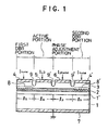
- Fig. 1 is a sectional view of a DBR variable-wavelength semiconductor laser element having a conventional structure when viewed from a plane parallel to a resonance direction of the element.
- an n-type cladding layer 1′, an active-optical waveguide layer 2, and a p-type cladding layer 3 are sequentially stacked on an n-type semiconductor substrate 1.
- a first DBR portion, an active portion, a phase adjustment portion, and a second DBR portion are juxtaposed in a laser resonance direction.
- electrodes, 4, 5, 6, and 4′ are independently formed.
- a common electrode 7 is formed on the bottom surface of the substrate 1.
- Grooves 9, 9′, and 9 ⁇ are formed at boundaries of these portions.
- Diffraction gratings 8 and 8′ are formed in the layer 2 of the first and second DBR portions.
- the phase adjustment portion adjusts the phase of light reflected by the DBR portions so as to cause this element to oscillate in a single mode.
- the phase can be adjusted in such a manner than a current I phase is injected from the electrode 6, and the refractive index of the layer 2 is changed by utilizing the plasma effect.
- a change ⁇ -p in oscillation wavelength can be expressed by: where n aeff and n peff are the effective refractive indices of the active portion and the phase adjustment portion, respectively, and l a , l p , and l b are the lengths of the active portion, the phase adjustment portion, and the DBR portion, respectively.
- equation (2) can yield a smaller ⁇ in unit of the same number of carriers than that of equation (1).
- the current I phase must be set to be higher than the current I tune .
- Japanese Patent Laid-Open Nos. 62-2213, 62-241387, 63-133105, and the like disclose techniques for forming a wavelength selective filter using a structure similar to that of the above-mentioned semiconductor laser.
- Fig. 2 is a side sectional view showing such an example of a conventional wavelength selective filter.
- a buffer layer 78, an optical waveguide layer 72, an active layer 71, and a cladding layer 79 are sequentially formed on a substrate 77.
- This multilayered structure is divided into a light gain portion 74, a phase control portion 75, and a DBR portion 76 in a light propagation direction. Electrodes 801, 802, and 803 from which currents can be independently injected are respectively formed on these portions.
- a diffraction grating 73 is formed in the optical waveguide layer 72 of the DBR portion.
- a carrier injection amount in order to realize stable wavelength selectivity and to assure sufficient crosstalk with a non-selected wavelength, a carrier injection amount must be limited.
- the plasma effect by carrier injection has an effect of decreasing the refractive index, while heat produced by carrier injection has an effect of increasing the refractive index.
- the refractive index is decreased with an increase in carrier injection amount, i.e., an increase in injection current, while the refractive index is increased due to heat produced by the current. Therefore, the refractive index is saturated to a predetermined value, and a tuning range of a selected wavelength is limited to a narrow range.
- a semiconductor laser element which can change an emission wavelength, comprising: a substrate; a laser resonator formed on the substrate, the resonator being formed by stacking semiconductor layers including an active layer and an optical waveguide layer of a superlattice structure, and the resonator including a first reflection portion, an active portion, a phase adjustment portion, and a second reflection portion which are juxtaposed in a resonance direction; diffraction gratings formed in the optical guide layer of the first and second reflection portions; and electrodes independently formed in the active portion, the phase adjustment portion, and the first and second reflection portions.
- the semiconductor laser element is driven by the following steps. That is, a method of driving the semiconductor laser element, comprises the steps of: injecting a current from the electrode of the active portion to the active layer to cause laser oscillation; injecting a current from the electrodes of the first and second reflection portions to change a refractive index of the optical waveguide layer, thereby changing a wavelength of light undergoing laser oscillation; and applying a reverse bias voltage to the electrode of the phase adjustment portion to change a refractive index of the optical waveguide layer by a quantum confinement Stark effect, thereby adjusting a phase of light undergoing laser oscillation.
- Fig. 3 is a sectional view showing the first embodiment of a semiconductor laser element according to the present invention when viewed from a plane parallel to a resonance direction.
- an n-type cladding layer 11′, an optical waveguide layer 20, an active layer 12, and a p-type cladding layer 13 are sequentially stacked on an n-type semiconductor substrate 11.
- These semiconductor layers constitute a laser resonator.
- a first DBR portion, an active portion, a phase adjustment portion, and a second DBR portion are juxtaposed in a resonance direction.
- the active layer 12 is present in only the active portion, and is removed from other portions.
- the optical waveguide layer 20 has a superlattice structure in which semiconductor thin films of two types having different band gaps are alternately stacked. Diffraction gratings 18 and 18′ are respectively formed in the optical waveguide layer 20 of the first and second DBR portions.
- grooves 19, 19′, and 19 ⁇ are formed at boundaries of these portions.
- An SiN layer 21 for covering the optical waveguide layer 20 is formed on the bottom portions of the grooves 19′ and 19 ⁇ .
- a common electrode 17 connected to a ground level is formed on the bottom surface of the substrate 11.
- a reverse bias voltage E phase is applied to a p-n junction of this element.
- a quantum confinement Stark effect occurs in the superlattice structure of the optical waveguide layer.
- This this effect the refractive index of the layer 20 is changed.
- a change in refractive index of about 10 ⁇ 2 can be expected.
- This change ⁇ n in refractive index is larger by ten times than a conventional change in refractive index of about 10 ⁇ 3 by the plasma effect. Since almost no current flows through the phase adjustment portion, no heat is generated, and a sufficiently large change in wavelength can be expected as compared to a conventional method. Since a large ⁇ n can be obtained, the length of the phase adjustment portion can be decreased. Since the decrease in length can decrease an internal loss, the threshold current of laser oscillation can be advantageously decreased.
- a semiconductor laser element shown in Fig. 3 was manufactured in the following process.
- An n-type Al w Ga 1-w As cladding layer 11′ was grown on an n-type GaAs substrate 11. 60- ⁇ thick GaAs and Al y Ga 1-y As layers were alternately stacked on the cladding layer to form an optical waveguide layer 20 having a superlattice structure. A GaAs active layer 12 was then grown on the layer 20. These semiconductor layers were consecutively grown by molecular beam epitaxy (MBE).
- MBE molecular beam epitaxy
- the active layer 12 was etched by chemical etching to the optical guide layer 20 to leave an active portion.
- An SiN coating layer 21 was formed on the resultant structure.
- the layer 21 was etched to leave formation regions for grooves 19′ and 19 ⁇ .
- Cyclic diffraction gratings 18 and 18′ were formed in DBR portions of the exposed optical waveguide layer 20 by a laser interference method.
- a p-type Al x Ga 1-x As cladding layer 13 was grown on the structure. In this case, since no Al x Ga 1-x As could be grown on the SiN layer 21, the grooves 19 and 19′ were consequently formed.
- a groove 19 was then formed to dry etching.
- the groove 19 can have a small depth since currents are supplied to the DBR portion and the active portion in the same direction, and an electrical isolation therebetween need not be enhanced.
- electrodes 14, 14′, 15, and 16 were formed by depositing an Au-Zn film.
- An Au-Sn film was deposited on the bottom surface of the substrate to form a common electrode 17.
- a length L a of the active portion, and a length L b of each of the first and second DBR portions were set to be 200 ⁇ m each.
- a length L p of the phase adjustment portion was set to be 20 ⁇ m, a width of L d of each of the grooves 19′ and 19 ⁇ was set to be 10 ⁇ m.
- the thickness of the active layer 12 was set to be 0.3 ⁇ m, the total thickness of the optical waveguide layer 20 was set to be 0.3 ⁇ m, and a pitch of the lattice was set to be about 2,500 ⁇ .
- the absorption end of an absorption spectrum of the waveguide is set near a laser oscillation wavelength ⁇ 0.
- the absorption spectrum curve is changed from a solid curve to a dotted curve by the quantum confinement Stark effect, the absorption end is changed from a point A to a point B.
- an absorption is enhanced, and a refractive index is considerably decreased.
- a large change in refractive index could occur to change an oscillation wavelength over a wide range.
- Fig. 5 is a sectional view showing the second embodiment of a semiconductor laser element according to the present invention when viewed from a plane parallel to a resonance direction.
- the element shown in Fig. 5 was manufactured following the same procedures as in Example 1.
- the structure of this example is substantially the same as that in Example 1 except that high-resistance regions 31 and 31′ are formed in the optical waveguide layer 20 on the bottom portions of the grooves 19′ and 19 ⁇ . Therefore, a detailed description of the respective portions will be omitted.
- the regions 31 and 31′ were formed by implanting oxygen ions into the bottom portions of the grooves 19′ and 19 ⁇ , and annealing the bottom portions.
- the optical characteristics of the regions 31 and 31′ were not changed very much as compared to other portions of the layer 20. With the regions 31 and 31′, currents flowing through the active portion and the DBR portions could be prevented from flowing into the phase adjustment portion, and a threshold current of laser oscillation could be further decreased. In addition, a fluctuation range of the Bragg wavelength could be widened.
- Fig. 6 is a sectional view showing the third embodiment according to the present invention.
- the structure shown in Fig. 6 includes an n-type GaAs substrate 41, an n-type Al w Ga 1-w As cladding layer 41′, an Al v Ga 1-v As active layer 42, a p-type Al x Ga 1-x As cladding layer 43, distributed diffraction gratings 48 and 48′, grooves 49′ and 49 ⁇ for enhancing electrical isolation, a waveguide layer 50 comprising a GaAs/Al y Ga 1-y As superlattice structure, a GaAs etching-stop layer 51, and high-resistance non-doped Al w ,Ga 1-w ,As layers 52 and 52′, for burying the grooves 49′ and 49 ⁇ .
- the n-type cladding layer 41′, the optical waveguide layer 50, the etching-stop layer 51, and the active layer 42 were successively grown on the n-type GaAs substrate 41 by a conventional MBE method. Thereafter, the active layer 42 was etched by chemical etching to the etching-stop layer 50 to leave an active portion.
- the cyclic diffraction gratings 48 and 48′ were formed in the DBR portions of the exposed optical waveguide layer 20 by a laser interference method.
- the Al x Ga 1-x As cladding layer 43 was grown on the resultant structure by an LPE method.
- the grooves 49′ and 49 ⁇ were formed to a depth enough to reach the etching-stop layer 51 by selective wet etching. These grooves 49′ and 49 ⁇ were buried with the non-doped Al w ,Ga 1-w ,As layers 52 and 52′ by LPE.
- an oscillation wavelength could be changed within the range of 0.835 to 0.825 ⁇ m.
- the grooves were buried with the AlGaAs layers to decrease a change in diffraction index distribution on a laser optical path. For this reason, light reflection or a loss occurring at two ends of the phase adjustment portion could be minimized, and single mode oscillation with a more stable output could be attained.
- a first cladding layer 62, an optical waveguide layer 63, and a second cladding layer 64 are formed on a substrate 61.
- the optical waveguide layer 63 comprises a superlattice structure in which 100- ⁇ thick GaAs well layers and AlAs barrier layers are alternately stacked.
- a diffraction grating 65 having a grating pitch ⁇ is formed on the upper portion of the second cladding layer 64.
- the wavelength of light to be filtered can be tuned by controlling an application voltage to the element.
- Fig. 8 is a graph showing the relationship between a wavelength of propagation light and an absorption coefficient in the element shown in Fig. 7.
- Fig. 9 is a graph showing the relationship between a wavelength and a fluctuation ratio ⁇ n of the refractive index in the element shown in Fig. 7. Curves disignated by (0) to (v) in Figs. 8 and 9 respectively represent results when when the following voltages were applied to the element.
- the fluctuation ratio ⁇ n of the refractive index shown in Fig. 9 was obtained from the following Kramers-Kronig relation using differences ⁇ between absorption coefficients in the state (0) and when the voltages (i) to (v) were applied: ( ⁇ : angular frequency of light)
- a wavelength is plotted along the abscissa, and an exiton absorption wavelength of a ground-level electron ie and a heavy hole hh is defined as ⁇ g .
- ⁇ g an exiton absorption wavelength of a ground-level electron ie and a heavy hole hh.
- ⁇ b 2 ⁇ n ⁇ Therefore, when ⁇ n ⁇ 0, ⁇ b ⁇ 0 is satisfied, and the reflection wavelength is shifted to a short wavelength side.
- a loss in the optical waveguide layer since the shifted wavelength approaches an absorption end, absorption is increased, and a loss becomes large. Furthermore, since the absorption end of the exiton is shifted to a long wavelength side by an applied electric field, a loss is further increased.
- Fig. 10 is a side sectional view showing a structure of the first embodiment of a wavelength selective filter according to the present invention
- Figs. 11 and 12 are graphs showing transmission characteristics of guided light.
- a first optical waveguide layer 83 was formed on the layer 82.
- the first optical waveguide layer 83 comprised a 0.11- ⁇ m thick superlattice structure in which 100- ⁇ thick Al 0.7 Ga 0.3 As well layers and 100- ⁇ thick Al 0.5 Ga 0.5 As barrier layers were alternately stacked.
- a 0.2- ⁇ m thick non-doped Al 0.3 Ga 0.7 As second waveguide layer 84 was formed on the layer 83.
- Gratings 85 having a pitch of 0.25 ⁇ m, for secondarily diffracting light in a wavelength range of 800 to 850 nm were formed on a portion (the left portion in Fig. 10) of the upper surface of the second waveguide layer 84.
- a pitch changing portion 86 whose pitch was offset by 0.12 ⁇ m to form a peak in a wavelength spectrum of transmission light was formed at the central portion of the gratings 85.
- waves reflected by the right and left gratings of the pitch changing portion 86 were shifted, and a peak appeared in a transmission spectrum by an etalon effect.
- an AuGe/Au electrode 892 was formed on the rear surface of the substrate 81.
- a 20- ⁇ m wide groove 80 was formed to reach the second waveguide layer 84 so that a voltage was applied to only a DBR portion A in which the gratings 85 were formed.
- wavelengths which are on a longer wavelength side than the exiton wavelength and always have a positive fluctuation ratio of the refractive index are selected to compensate for a loss caused by absorption.
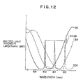
- Fig. 11 shows wavelength dependency of transmittance of light guided when only the DBR portion A of this embodiment is extracted.
- a solid curve represents a result when an application voltage is 0, and a broken curve represents a result when an application voltage is 3 V.
- a solid curve represents an emitted light intensity when no voltage was applied.
- a broken curve and an alternate long and short dashed curve represent results when voltages of 1.5 V and 3 V were applied, respectively.
- a peak intensity upon application of a voltage of 3 V is attenuated by only 0.2 dB as compared to an intensity obtained when no voltage is applied.
- Fig. 13 is a side sectional view showing a structure of the second embodiment of a wavelength selective filter according to the present invention, and Fig. 14 shows transmission characteristics of guided light of the filter.
- the same reference numerals in Fig. 13 denote the same parts as in Fig. 10, and a detailed description thereof will be omitted.
- the pitch changing portion 86 is formed in the gratings 85 to generate a peak in a transmission spectrum.
- the capping layer 88 and the electrode 891 shown in Fig. 10 are divided by a groove 91 to form divided capping layers 981 and 982 and divided electrodes 991 and 992.
- Different voltages are applied from these electrodes 991 and 992 to the first waveguide layer 83 of the superlattice structure, thereby generating a peak in the transmission spectrum. For this reason, no pitch changing portion 86 is formed in gratings 95.
- Other structures are the same as those in the first embodiment.
- a solid curve represents a state (state I) when no voltage was applied to the divided electrodes 991 and 992 in the same manner as for the solid curve in Fig. 12.
- a broken curve and an alternate long and short dashed curve represent states when a voltage of 3 V was applied to only the divided electrode 991 (state II) and when a voltage of 3 V was applied to the divided electrodes 991 and 992 (state III).
- a peak in the state I was shifted by 2 ⁇ toward a short wavelength side in the state II, and was shifted by 2 nm toward a long wavelength side in the state III as in the first embodiment.
- the spectrum curve was further shifted by 2 ⁇ toward a long wavelength side, as represented by an alternate long and two short dashed curve in Fig. 14.
- a plurality of peak wavelengths can be formed within a stop bandwidth ⁇ s .
- a wavelength selection range of 2.4 nm as a whole can be obtained, and can be further widened.
- the electrode is divided into two sections. When the number of divided electrodes is increased, finer wavelength selection can be performed, and this invention also incorporates this structure.
- an increase in absorption coefficient in the DBR portion caused by the QCSE is compensated for by shifting guided light toward a long wavelength side in the optical waveguide portion.
- an increase in absorption coefficient may be compensated for by forming a light gain portion. This embodiment will be described below.
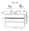
- Fig. 15 is a side sectional view showing the third embodiment of a wavelength selective filter.
- a protective photoresist was applied to a portion excluding a portion corresponding to a DBR portion 22 in order to form the DBR portion 22 on the portion of the second optical waveguide layer 105. Thereafter, a second photoresist layer was formed to the entire surface including the portion 22. Subsequently, the portion 22 was subjected to two-beam interference exposure using an He-Cd laser, and was developed to form photoresist gratings having a pitch of about 0.24 ⁇ m. Grating-like corrugations were formed on the upper surface of the second optical waveguide layer 105 by an RIBE (reactive ion beam etching) method using the photoresist as a mask. Thereafter, all the photoresist layers were removed.
- RIBE reactive ion beam etching
- the DBR portion 22 was formed. Subsequently, a p-type Al 0.5 Ga 0.5 As second cladding layer 106 and a p+-type GaAs contact layer 107 were sequentially formed on the resultant structure by an LPE method. An Au/Cr layer serving as electrodes was deposited on the upper portion of the contact layer 107. The Au/Cr layer was divided into a first electrode 108 for the DBR portion, a third electrode 109 as an unnecessary current preventing means for trapping carriers, and a second electrode 110 for a light gain portion, as shown in Fig. 15. The contact layer 107 was also etched accordingly to be divided into three sections. The multilayered structure was polished, and an Au/AuGe layer serving as a fourth electrode 111 was deposited on the rear surface of the substrate 101 to perform alloying.
- a ZrO2 anti-reflection film 112 for preventing random reflection was formed on an entrance/exit end face of the formed element on the side of the DBR portion. Thereafter, this element was fixed in a holder, and power sources were connected to the electrodes.
- Fig. 16 shows a change in transmittance in the DBR portion to have the Bragg wavelength ⁇ B as the central wavelength.
- a transmittance and a reflectance considerably vary according to the wavelength of input light, and at a wavelength sufficiently separated from the Bragg wavelength ⁇ B , input light is transmitted without causing diffraction or reflection.
- the diffraction grating is not a primary diffraction grating, radiation light is diffracted in the vertical direction of the diffraction grating. In any case, light in such a wavelength region is transmitted through the DBR portion.
- a stop band 221 having a bandwidth of about several to several tens of ⁇ is formed to have the Bragg wavelength ⁇ B as the central wavelength.
- a transmission wavelength region 222 having a small spectral width is formed at an arbitrary position in the stop band 221.
- the transmission wavelength region 222 is shifted according to the phase of the end face of the DBR portion.
- the transmission wavelength region 222 in the stop band 221 is arbitrarily controlled to obtain a wavelength variable optical filter.
- a method of shifting the region 222 a method of splitting a portion of the DBR portion to control optical phase shift, a method of controlling the phase at the end face of the DBR portion, a method of controlling an effective pitch of the diffraction grating in the DBR portion, and the like are available. With these methods, the refractive index of a medium is controlled.
- a voltage -V t is applied to the DBR portion 22, and a forward current I g is injected into the light gain portion 23.
- a forward current I g is injected into the light gain portion 23.
- an application voltage serves as a reverse bias for a p-i-n junction
- no carrier is injected, and an electric field is applied to the first optical waveguide layer 104 as an i-type layer.
- the refractive index of the layer 104 in the DBR portion is changed by the QCSE, and an absorption spectrum is also changed. Therefore, the Bragg wavelength of the DBR portion 22 is shifted. In this manner, a selected wavelength is tuned.
- the QCSE causes a large change in refractive index and also causes a large change in absorption coefficient.
- a forward bias voltage is applied to the light gain portion 23 to inject a carrier (current I g ), thus providing a light gain.
- the injection current I g is controlled to compensate for attenuation of light in the DBR portion 22, and to obtain a stable selected transmittance (or amplification factor) regardless of a tuned wavelength.
- wavelength tuning in the DBR portion is performed by the QCSE, so that it is possible to theoretically obtain a large change in refractive index, i.e., a wide tuning range without causing heat generation.
- a change in absorption spectrum or a large absorbed light amount as the disadvantage of the QCSE can be eliminated by forming the light gain portion 23 in the resonator to be adjacent to the DBR portion 22.
- the light gain portion 23 a change in refractive index due to the plasma effect is caused by the injection current as well as a light gain, thus changing the phase at the boundary with the DBR portion 22.
- a selected wavelength is tuned by a voltage applied to the DBR portion 22 and a current injected into the light gain portion 23, the voltage applied to the DBR portion 22 is dominant in tuning of the selected wavelength since the change in refractive index caused by the QCSE is large and the effective pitch of corrugations is controlled by directly applying a voltage to the DBR portion 22.
- a voltage changing within the range of 0 V to -5 V was applied from the first electrode 108 to the DBR portion 22 to change a transmission wavelength range.
- a current changing within the range of 20 to 80 mA was injected from the second electrode 110 to the light gain portion so as to control to obtain a constant transmittance (or light gain) upon tuning of a wavelength.
- a voltage to be applied to the third electrode 109 for trapping a carrier was almost the same as that to be applied to the first electrode, thereby preventing the flow of carriers to the DBR portion 22.
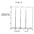
- Fig. 17 shows results obtained by measuring a transmission spectrum with a wavelength variable light source using the above-mentioned element.
- a reverse bias voltage was applied to the DBR portion, the position of a transmission wavelength was shifted.
- current injection was performed in the light gain portion 23, as described above, to compensate for a change in absorption coefficient of the DBR portion 22 caused upon application of the reverse bias voltage.
- a transmittance or amplification factor
- the wavelength tuning range has a width of 10 ⁇ or more, and has a possibility of being able to be further widened. Since the QCSE is used in wavelength tuning, a response time can be as very short as 1 ns or less.
- a reverse bias voltage is applied to the third electrode 109 to prevent the flow of carriers from the portion 23 to the portion 22.
- the following method may be proposed.
- the contact layer 107 i.e., one electrode is separated from the other electrode.
- Fe or O2 is doped in a portion between the two electrodes to obtain a high-resistance portion.
- a portion between the electrodes is temporarily etched, and a non-doped region is regrown on the resultant gap portion.
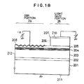
- Fig. 18 is a side sectional view showing a structure of the fourth embodiment of a wavelength selective filter according to the present invention.
- a filter which can perform the same operation as in the embodiment shown in Fig. 15 is realized by a simpler manufacturing process.
- a light gain portion 25 the resultant structure was etched to a depth enough to expose the cladding layer 206 except for this portion, thereby exposing the second optical waveguide layer 205.
- a DBR portion 24 was formed.
- An Au/Cr layer serving as a second electrode 210 was formed on the contact layer 207 as the light gain portion.
- a third electrode 211 was formed on the lower surface of the substrate 201 to perform alloying.
- An Au first electrode 208 was deposited on the DBR portion 24.
- an interval between the DBR portion 24 and the light gain portion 25 was about 30 ⁇ m, and an anti-reflection film 212 was formed on the end face on the formation side of the DBR portion 24 as in the third embodiment.
- the element manufactured in this manner was fixed in a holder, and power sources were connected to the electrodes.
- the reason why no carrier trapping electrode is formed is that p-type layers (corresponding to the second cladding layer 106 and the contact layer 107 in Fig. 15) of the DBR portion 24 are removed unlike in the light gain portion 25. For this reason, the flow of carriers could be satisfactorily prevented by slight electrode isolation, and the number of steps in the manufacture could be reduced. Since the first electrode 208 was directly formed on the DBR portion 24, a waveguide absorption loss caused by a metal film occurred. For this reason, an injection current must be slightly increased as compared to that in the third embodiment. The evaluation results of the element were the same as those of the third embodiment.
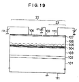
- Fig. 19 is a side sectional view showing a structure of the fifth embodiment of a wavelength selective filter according to the present invention.
- the same reference numerals in Fig. 19 denote the same parts as in Fig. 15, and a detailed description thereof will be omitted.
- a first optical waveguide layer 504 comprising an MQW consisting of 70- ⁇ thick GaAs layers and 100- ⁇ -thick i-type Al 0.3 Ga 0.7 As layers is used in place of the first optical waveguide layer 104 in the third embodiment, and a second optical waveguide layer 505 in which corrugations are formed on the entire surface is used in place of the second waveguide layer 105.
- Other structures are the same as those in the third embodiment.
- the electrode is split into three electrodes as in the third embodiment, and an anti-reflection film is formed on two end faces, i.e., input and output surfaces.
- a reverse voltage -V t ranging from 0 to -5 V was applied to the first electrode 108 on the DBR portion 22, and the third electrode 109 for trapping carriers, and a current ranging from 10 to 70 mA was injected into the light gain portion, thereby performing wavelength tuning.
- This embodiment employs a so-called distributed feedback (DFB) structure wherein a light gain is given even in the DBR portion.
- the principal tuning mechanism of the previous embodiment is to control an effective refractive index of the diffraction grating, while in this embodiment, since phase shift occurs at the central portion of the DBR portion, a wavelength tuning range can be further expanded due to an effect of shift of a transmission wavelength region in the stop band.
- the tuning range could be about 15 ⁇ or more.
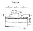
- Fig. 20 is a side sectional view showing a structure of the sixth embodiment of a wavelength selective filter according to the present invention.
- the same reference numerals in Fig. 20 denote the same parts as in Fig. 15, and a detailed description thereof will be omitted.
- DBR portions are respectively formed on two sides of a light gain portion.
- a second optical waveguide layer 605 on which corrugations were formed at two end portions was used in place of the second optical waveguide layer 105 in the third embodiment, and a second cladding layers 606 and a contact layer 607 were stacked on the central portion of the layer 605.
- First and second electrodes 608 and 610 were respectively formed on the upper portions of the corrugations, and a third electrode 609 was formed on the upper portion of the contact layer 607.
- An anti-reflection film (not shown) was formed on two entrance and exit end faces. Other structures are the same as those in the third embodiment.
- a selected wavelength is tuned by controlling the effective pitch of corrugations and controlling a phase shift amount at the central portion in the same manner as in the fifth embodiment. Since the phase shift amount is controlled by changing a light gain, tuning of a selected wavelength mainly depends on control of a reverse voltage -V t to be applied to the DBR portion 22.
- a wavelength tuning range of this embodiment is the same as that in the fourth embodiment. However, in this embodiment, since the DBR portions are formed at two end portions of a resonator, a full width at half maximum of the transmission wavelength region is small, and the number of channels of wavelength tuning can be essentially increased.
- the semiconductor layers consist of AlGaAs but may be formed of other materials such as InGaAsP.
- the present invention incorporates such applications within the scope of the appended claims.
- a semiconductor laser element capable of changing an oscillation wavelength over a wide range without increasing a threshold current is disclosed.
- a wavelength selective filter capable of changing a selected wavelength over a wide range is also disclosed.
- the semiconductor laser element has a substrate and a laser resonator formed on the substrate by stacking semiconductor layers including an active layer and an optical waveguide layer of a superlattice structure.
- the resonator includes a first reflection portion, an active portion, a phase adjustment portion and second reflection portion which are juxtaposed in a resonance direction. Diffraction gratings are formed in the optical guide layer of the first and second reflection portions. Electrodes are independently formed in the active portion, the phase adjustment portion and the first and second reflection portions. Further, a method for driving the semiconductor laser is disclosed.
Applications Claiming Priority (6)
| Application Number | Priority Date | Filing Date | Title |
|---|---|---|---|
| JP1083928A JP2703619B2 (ja) | 1989-04-04 | 1989-04-04 | 波長可変半導体レーザ |
| JP83928/89 | 1989-04-04 | ||
| JP1180396A JP2854330B2 (ja) | 1989-07-14 | 1989-07-14 | 波長可変光フィルタ |
| JP180396/89 | 1989-07-14 | ||
| JP184580/89 | 1989-07-19 | ||
| JP18458089A JP2788760B2 (ja) | 1989-07-19 | 1989-07-19 | 選択波長可変フィルタ |
Publications (3)
| Publication Number | Publication Date |
|---|---|
| EP0391334A2 true EP0391334A2 (de) | 1990-10-10 |
| EP0391334A3 EP0391334A3 (de) | 1991-08-28 |
| EP0391334B1 EP0391334B1 (de) | 1994-08-31 |
Family
ID=27304372
Family Applications (1)
| Application Number | Title | Priority Date | Filing Date |
|---|---|---|---|
| EP90106344A Expired - Lifetime EP0391334B1 (de) | 1989-04-04 | 1990-04-03 | Halbleiterlaser mit veränderbarer Emissionswellenlänge und selektives Wellenlängenfitter und Verfahren zum Betrieb derselben |
Country Status (3)
| Country | Link |
|---|---|
| US (1) | US5155736A (de) |
| EP (1) | EP0391334B1 (de) |
| DE (1) | DE69011921T2 (de) |
Cited By (4)
| Publication number | Priority date | Publication date | Assignee | Title |
|---|---|---|---|---|
| US5416866A (en) * | 1992-08-26 | 1995-05-16 | Telefonaktiebolaget L M Ericsson | Optical waveguide/grating device for filtering optical wavelengths |
| FR2737942A1 (fr) * | 1995-08-18 | 1997-02-21 | Delorme Franck | Composant d'emission laser accordable en longueur d'onde par variation d'absorption |
| EP0847116A2 (de) * | 1992-03-06 | 1998-06-10 | Nippon Telegraph And Telephone Corporation | Verteiler Reflektor und Halbleiterlaser mit abstimmbarer Wellenlänge |
| EP1218973A1 (de) * | 1999-09-03 | 2002-07-03 | The Regents Of The University Of California | Abstimmbare laser-quelle mit integriertem optischen modulator |
Families Citing this family (17)
| Publication number | Priority date | Publication date | Assignee | Title |
|---|---|---|---|---|
| CA2101411C (en) * | 1992-08-14 | 2003-06-10 | Jean-Pierre Weber | Tunable optical filter |
| JP3086767B2 (ja) * | 1993-05-31 | 2000-09-11 | 株式会社東芝 | レ−ザ素子 |
| JPH0738204A (ja) * | 1993-07-20 | 1995-02-07 | Mitsubishi Electric Corp | 半導体光デバイス及びその製造方法 |
| US6198814B1 (en) | 1997-10-17 | 2001-03-06 | Debra Ann Marie Gill | System and method for entering call outcome records in a computer database in an outbound predictive dialing application |
| CA2405852A1 (en) * | 2000-05-04 | 2001-11-08 | Agility Communications, Inc. | Improved mirror and cavity designs for sampled-grating distributed bragg reflector lasers |
| US7061943B2 (en) * | 2000-06-29 | 2006-06-13 | Agility Communications, Inc. | Controller calibration for small form factor sampled grating distributed Bragg reflector laser |
| US6728290B1 (en) * | 2000-09-13 | 2004-04-27 | The Board Of Trustees Of The University Of Illinois | Current biased dual DBR grating semiconductor laser |
| JP2002094176A (ja) * | 2000-09-14 | 2002-03-29 | Mitsubishi Electric Corp | レーザ装置 |
| GB2373632B (en) * | 2001-03-19 | 2005-04-27 | Marconi Caswell Ltd | Tuneable laser |
| WO2002093695A2 (en) * | 2001-05-15 | 2002-11-21 | Agility Communications, Inc. | Sampled grating distributed bragg reflector laser controller |
| GB2381123B (en) * | 2001-10-17 | 2005-02-23 | Marconi Optical Components Ltd | Tuneable laser |
| JP4104925B2 (ja) * | 2002-07-10 | 2008-06-18 | 三菱電機株式会社 | 波長可変半導体レーザの波長制御装置 |
| US7295589B2 (en) * | 2003-02-15 | 2007-11-13 | Avago Technologies Fiber (Singapore) Pte Ltd | Frequency modulated vertical cavity laser |
| JP2013168500A (ja) * | 2012-02-15 | 2013-08-29 | Mitsubishi Electric Corp | 光半導体装置 |
| JP2018182306A (ja) * | 2017-04-17 | 2018-11-15 | 浜松ホトニクス株式会社 | 光半導体素子、及び光半導体素子の駆動方法 |
| KR102368946B1 (ko) * | 2017-12-15 | 2022-03-04 | 한국전자통신연구원 | 파장 가변 레이저 장치 및 이를 제조하는 방법 |
| KR102495786B1 (ko) * | 2019-01-04 | 2023-02-06 | 후아웨이 테크놀러지 컴퍼니 리미티드 | 반도체 레이저, 광 전송기 컴포넌트, 광 회선 단말 및 광 네트워크 유닛 |
Citations (7)
| Publication number | Priority date | Publication date | Assignee | Title |
|---|---|---|---|---|
| JPS60133777A (ja) * | 1983-12-22 | 1985-07-16 | Nippon Telegr & Teleph Corp <Ntt> | 半導体発光装置 |
| EP0173269A2 (de) * | 1984-08-24 | 1986-03-05 | Nec Corporation | Halbleiterlaservorrichtung |
| EP0269061A2 (de) * | 1986-11-26 | 1988-06-01 | Nec Corporation | Optische Filtervorrichtung |
| EP0287065A2 (de) * | 1987-04-14 | 1988-10-19 | Nec Corporation | Optische Filtervorrichtung |
| JPS63299291A (ja) * | 1987-05-29 | 1988-12-06 | Kokusai Denshin Denwa Co Ltd <Kdd> | 半導体レ−ザ |
| EP0300790A2 (de) * | 1987-07-21 | 1989-01-25 | Kokusai Denshin Denwa Kabushiki Kaisha | Halbleiterlaser |
| JPS6449293A (en) * | 1987-08-19 | 1989-02-23 | Nec Corp | Semiconductor laser with variable wavelength |
Family Cites Families (5)
| Publication number | Priority date | Publication date | Assignee | Title |
|---|---|---|---|---|
| JPS63150986A (ja) * | 1986-12-15 | 1988-06-23 | Sharp Corp | 半導体レ−ザ |
| JPH0656908B2 (ja) * | 1987-03-31 | 1994-07-27 | 日本電信電話株式会社 | 波長変換素子 |
| JP2749038B2 (ja) * | 1987-07-31 | 1998-05-13 | 株式会社日立製作所 | 波長可変半導体レーザ |
| JP2825508B2 (ja) * | 1987-10-09 | 1998-11-18 | 株式会社日立製作所 | 半導体レーザ装置および光通信システム |
| JPH084186B2 (ja) * | 1987-10-28 | 1996-01-17 | 国際電信電話株式会社 | 半導体レーザ |
-
1990
- 1990-04-03 DE DE69011921T patent/DE69011921T2/de not_active Expired - Fee Related
- 1990-04-03 EP EP90106344A patent/EP0391334B1/de not_active Expired - Lifetime
-
1991
- 1991-11-14 US US07/790,832 patent/US5155736A/en not_active Expired - Lifetime
Patent Citations (7)
| Publication number | Priority date | Publication date | Assignee | Title |
|---|---|---|---|---|
| JPS60133777A (ja) * | 1983-12-22 | 1985-07-16 | Nippon Telegr & Teleph Corp <Ntt> | 半導体発光装置 |
| EP0173269A2 (de) * | 1984-08-24 | 1986-03-05 | Nec Corporation | Halbleiterlaservorrichtung |
| EP0269061A2 (de) * | 1986-11-26 | 1988-06-01 | Nec Corporation | Optische Filtervorrichtung |
| EP0287065A2 (de) * | 1987-04-14 | 1988-10-19 | Nec Corporation | Optische Filtervorrichtung |
| JPS63299291A (ja) * | 1987-05-29 | 1988-12-06 | Kokusai Denshin Denwa Co Ltd <Kdd> | 半導体レ−ザ |
| EP0300790A2 (de) * | 1987-07-21 | 1989-01-25 | Kokusai Denshin Denwa Kabushiki Kaisha | Halbleiterlaser |
| JPS6449293A (en) * | 1987-08-19 | 1989-02-23 | Nec Corp | Semiconductor laser with variable wavelength |
Non-Patent Citations (4)
| Title |
|---|
| PATENT ABSTRACTS OF JAPAN, vol. 13, no. 132 (E-736)[3480], 31st March 1989; & JP-A-63 299 291 (KOKUSAI DENSHIN DENWA CO. LTD) * |
| PATENT ABSTRACTS OF JAPAN, vol. 13, no. 248 (E-770), 23rd February 1989; & JP-A-1 049 293 (NEC CORP.) 23-02-1989 * |
| PATENT ABSTRACTS OF JAPAN, vol. 9, no. 295 (E-360)[2018], 21st November 1985; & JP-A-60 133 777 (NIPPON DENSHIN DENWA KOSHA) 16-07-1985 * |
| TRANSACTIONS OF THE I.E.C.E. OF JAPAN, vol. E68, no. 12, December 1985, pages 788-790, Tokyo, JP; Y. TOHMORI et al.: "Wavelength tunable 1.5mum GaInAsP/InP bundle-integrated-guide distributed bragg reflector (BIG-DBR) lasers" * |
Cited By (11)
| Publication number | Priority date | Publication date | Assignee | Title |
|---|---|---|---|---|
| EP0847116A2 (de) * | 1992-03-06 | 1998-06-10 | Nippon Telegraph And Telephone Corporation | Verteiler Reflektor und Halbleiterlaser mit abstimmbarer Wellenlänge |
| EP0847116A3 (de) * | 1992-03-06 | 1998-09-02 | Nippon Telegraph And Telephone Corporation | Verteiler Reflektor und Halbleiterlaser mit abstimmbarer Wellenlänge |
| US5416866A (en) * | 1992-08-26 | 1995-05-16 | Telefonaktiebolaget L M Ericsson | Optical waveguide/grating device for filtering optical wavelengths |
| DE4328777B4 (de) * | 1992-08-26 | 2007-11-22 | Telefonaktiebolaget Lm Ericsson (Publ) | Optische Filtervorrichtung |
| FR2737942A1 (fr) * | 1995-08-18 | 1997-02-21 | Delorme Franck | Composant d'emission laser accordable en longueur d'onde par variation d'absorption |
| GB2304423A (en) * | 1995-08-18 | 1997-03-19 | France Telecom | Tuneable wavelength laser |
| US5838714A (en) * | 1995-08-18 | 1998-11-17 | France Telecom | Tunable wavelength laser emission components |
| GB2304423B (en) * | 1995-08-18 | 1999-05-12 | France Telecom | Tunable wavelength laser emission components |
| EP1218973A1 (de) * | 1999-09-03 | 2002-07-03 | The Regents Of The University Of California | Abstimmbare laser-quelle mit integriertem optischen modulator |
| EP1218973A4 (de) * | 1999-09-03 | 2005-11-16 | Univ California | Abstimmbare laser-quelle mit integriertem optischen modulator |
| US7342950B1 (en) | 1999-09-03 | 2008-03-11 | The Regents Of The University Of California | Tunable laser source with integrated optical modulator |
Also Published As
| Publication number | Publication date |
|---|---|
| EP0391334B1 (de) | 1994-08-31 |
| DE69011921D1 (de) | 1994-10-06 |
| US5155736A (en) | 1992-10-13 |
| DE69011921T2 (de) | 1995-03-02 |
| EP0391334A3 (de) | 1991-08-28 |
Similar Documents
| Publication | Publication Date | Title |
|---|---|---|
| US5088097A (en) | Semiconductor laser element capable of changing emission wavelength, and method of driving the same | |
| EP0391334B1 (de) | Halbleiterlaser mit veränderbarer Emissionswellenlänge und selektives Wellenlängenfitter und Verfahren zum Betrieb derselben | |
| EP0606093B1 (de) | Integrierte optische Halbleiteranordnung und Herstellungsverfahren | |
| EP0495413B1 (de) | Licht-Detektionsvorrichtung mit Beugungsgitter | |
| JP4643794B2 (ja) | 半導体発光素子 | |
| US5250462A (en) | Method for fabricating an optical semiconductor device | |
| US5220573A (en) | Optical apparatus using wavelength selective photocoupler | |
| EP0431527A2 (de) | Optisches Kopplergerät mit wellenlängeselektivem optischem Koppler | |
| US5289484A (en) | Laser diode | |
| JPH07183622A (ja) | 反射性同調可能レーザー | |
| EP0378098B1 (de) | Optische Halbleitervorrichtung | |
| US5661741A (en) | Semiconductor light emitting device, laser amplifier, and integrated light amplifier and wavelength variable filter | |
| US6594298B2 (en) | Multi-wavelength semiconductor laser array and method for fabricating the same | |
| EP0661783B1 (de) | Verfahren zur Herstellung eines integrierten, optischen Halbleiterschaltkreises | |
| EP0386797B1 (de) | Photodetektor mit wellenlängenselektivem optischem Koppler | |
| EP0533485B1 (de) | Halbleiter-Vorrichtung und Methode zu deren Herstellung | |
| US4775980A (en) | Distributed-feedback semiconductor laser device | |
| EP0287065B1 (de) | Optische Filtervorrichtung | |
| GB2303739A (en) | Widely matchable sample grating distributed Bragg reflector laser | |
| EP0479279A2 (de) | Halbleiterlaser mit verteilter Rückkoppelung | |
| EP0687938B1 (de) | Nicht-lineare optische Halbleitervorrichtung | |
| EP0316194B1 (de) | Filter mit abstimmbarer Wellenlänge | |
| JPH06152052A (ja) | 多重量子井戸型半導体レーザ | |
| US6363093B1 (en) | Method and apparatus for a single-frequency laser | |
| JP2854330B2 (ja) | 波長可変光フィルタ |
Legal Events
| Date | Code | Title | Description |
|---|---|---|---|
| PUAI | Public reference made under article 153(3) epc to a published international application that has entered the european phase |
Free format text: ORIGINAL CODE: 0009012 |
|
| AK | Designated contracting states |
Kind code of ref document: A2 Designated state(s): DE FR GB |
|
| 17P | Request for examination filed |
Effective date: 19901221 |
|
| PUAL | Search report despatched |
Free format text: ORIGINAL CODE: 0009013 |
|
| AK | Designated contracting states |
Kind code of ref document: A3 Designated state(s): DE FR GB |
|
| 17Q | First examination report despatched |
Effective date: 19930706 |
|
| GRAA | (expected) grant |
Free format text: ORIGINAL CODE: 0009210 |
|
| AK | Designated contracting states |
Kind code of ref document: B1 Designated state(s): DE FR GB |
|
| REF | Corresponds to: |
Ref document number: 69011921 Country of ref document: DE Date of ref document: 19941006 |
|
| ET | Fr: translation filed | ||
| PLBE | No opposition filed within time limit |
Free format text: ORIGINAL CODE: 0009261 |
|
| STAA | Information on the status of an ep patent application or granted ep patent |
Free format text: STATUS: NO OPPOSITION FILED WITHIN TIME LIMIT |
|
| 26N | No opposition filed | ||
| REG | Reference to a national code |
Ref country code: GB Ref legal event code: IF02 |
|
| PGFP | Annual fee paid to national office [announced via postgrant information from national office to epo] |
Ref country code: GB Payment date: 20040331 Year of fee payment: 15 |
|
| PGFP | Annual fee paid to national office [announced via postgrant information from national office to epo] |
Ref country code: FR Payment date: 20040408 Year of fee payment: 15 |
|
| PGFP | Annual fee paid to national office [announced via postgrant information from national office to epo] |
Ref country code: DE Payment date: 20040415 Year of fee payment: 15 |
|
| PG25 | Lapsed in a contracting state [announced via postgrant information from national office to epo] |
Ref country code: GB Free format text: LAPSE BECAUSE OF NON-PAYMENT OF DUE FEES Effective date: 20050403 |
|
| PG25 | Lapsed in a contracting state [announced via postgrant information from national office to epo] |
Ref country code: DE Free format text: LAPSE BECAUSE OF NON-PAYMENT OF DUE FEES Effective date: 20051101 |
|
| GBPC | Gb: european patent ceased through non-payment of renewal fee |
Effective date: 20050403 |
|
| PG25 | Lapsed in a contracting state [announced via postgrant information from national office to epo] |
Ref country code: FR Free format text: LAPSE BECAUSE OF NON-PAYMENT OF DUE FEES Effective date: 20051230 |
|
| REG | Reference to a national code |
Ref country code: FR Ref legal event code: ST Effective date: 20051230 |