EP0384286A1 - Charge coupled device free from after image due to residual electric charges - Google Patents
Charge coupled device free from after image due to residual electric charges Download PDFInfo
- Publication number
- EP0384286A1 EP0384286A1 EP90102894A EP90102894A EP0384286A1 EP 0384286 A1 EP0384286 A1 EP 0384286A1 EP 90102894 A EP90102894 A EP 90102894A EP 90102894 A EP90102894 A EP 90102894A EP 0384286 A1 EP0384286 A1 EP 0384286A1
- Authority
- EP
- European Patent Office
- Prior art keywords
- impurity regions
- transfer gate
- electric converting
- photo electric
- narrow
- Prior art date
- Legal status (The legal status is an assumption and is not a legal conclusion. Google has not performed a legal analysis and makes no representation as to the accuracy of the status listed.)
- Granted
Links
- 239000012535 impurity Substances 0.000 claims abstract description 43
- 238000012546 transfer Methods 0.000 claims abstract description 38
- 239000004065 semiconductor Substances 0.000 claims description 12
- 239000000758 substrate Substances 0.000 claims description 12
- 230000003287 optical effect Effects 0.000 abstract description 6
- 230000005855 radiation Effects 0.000 abstract description 6
- 238000005036 potential barrier Methods 0.000 abstract description 4
- 108091006146 Channels Proteins 0.000 description 15
- 108010075750 P-Type Calcium Channels Proteins 0.000 description 6
- 230000003247 decreasing effect Effects 0.000 description 3
- 229910052729 chemical element Inorganic materials 0.000 description 2
- 230000009467 reduction Effects 0.000 description 2
- 230000001419 dependent effect Effects 0.000 description 1
- 238000010586 diagram Methods 0.000 description 1
- 238000002955 isolation Methods 0.000 description 1
- 230000007246 mechanism Effects 0.000 description 1
- 238000012986 modification Methods 0.000 description 1
- 230000004048 modification Effects 0.000 description 1
- 230000010363 phase shift Effects 0.000 description 1
- 230000003334 potential effect Effects 0.000 description 1
- 239000007787 solid Substances 0.000 description 1
Images


Classifications
-
- H—ELECTRICITY
- H01—ELECTRIC ELEMENTS
- H01L—SEMICONDUCTOR DEVICES NOT COVERED BY CLASS H10
- H01L27/00—Devices consisting of a plurality of semiconductor or other solid-state components formed in or on a common substrate
- H01L27/14—Devices consisting of a plurality of semiconductor or other solid-state components formed in or on a common substrate including semiconductor components sensitive to infrared radiation, light, electromagnetic radiation of shorter wavelength or corpuscular radiation and specially adapted either for the conversion of the energy of such radiation into electrical energy or for the control of electrical energy by such radiation
- H01L27/144—Devices controlled by radiation
- H01L27/146—Imager structures
- H01L27/148—Charge coupled imagers
- H01L27/14831—Area CCD imagers
Definitions
- This invention relates to a charge coupled device and, more particularly, to the configuration of a photo electric converting element.
- a solid state line sensor is implemented by a charge coupled device and used as an image sensor associated with an automatic focus controlling mechanism of a camera or incorporated in a facsimile machine.
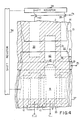
- Fig. 1 shows the layout of a prior art charge coupled device fabricated on a p-type semiconductor substrate 1, and a p-type channel stopper 2 provides an electrical isolation between adjacent photo electric converting elements 3 and 4 and a shift registor 5.
- the p-type channel stopper 2 is indicated by hatch lines for better understanding.
- each of the photo-electric converting elements 3 and 4 is implemented by the p-n junction type photo diode, and the photo electric converting element 4 is, by way of example, formed by an n-type impurity region 6 partially overlapped with a p-type impurity region 7.
- the n-type impurity region 6 is reversely biased with respect to the p-type semiconductor substrate 1.
- an n-type impurity region 8 which forms the shift registor 5 together with transfer gate electrodes 9, 10, 11 and 12 embedded in an insulating film 13 in a partially overlapping manner.
- the transfer gate electrodes 9 and 10 are supplied with a first phase clock pulse CL1, and a second phase clock pulse CL2 is fed to the transfer gate electrodes 11 and 12.
- the shift registor 5 thus arranged transfers a data signal in the form of electric charges in synchronization with the two phase clock signal in the left direction of Fig. 1.
- Photo shield plates 14 and 15 are provided on the insulating film 13 and are spaced from each other for exposing a part of photo electric converting elements 3 and 4 to an optical radiation carrying photo images, and parts of the optical radiation are converted into electric charges the amounts of which are dependent to the respective intensities of the parts of the optical radiation.
- a transfer gate electrode 16 allows the electric charges to flow into the shift registor 5.
- the transfer gate electrode 16 is partially overlapped with the n-type impurity region 6 at a overlapping area L encircled by dash lines 17, and the edge of the transfer gate electrode 9 extends below the transfer gate electrode 16.
- the electric charges accumulated in the n-type impurity region 6 are read out to the shift registor 5 in the presence of a transfer pulse Pt of a high voltage level fed to the transfer gate electrode 16, and the shift registor 5 transfers the electric charges in synchronization with the two phase shift clock signal as described above.
- the residual electric charges may be reduced by decreasing the overlapping area to a certain extent allowed in consideration of a nesting tolerance. However, this approach never satisfies the user.
- the present invention proposes to decrease a leading end portion of an n-type impurity region in width to a certain extent preventing the n-type impurity region from a narrow channel phenomenon.
- a charge coupled device fabricated on a lightly doped semiconductor substrate of a first conductivity type, comprising: a) a plurality of photo electric converting elements implemented by a plurality of first impurity region of a second conductivity type formed in the semiconductor substrate and a plurality of second impurity regions of the first conductivity type respectively formed in the first impurity regions so as to form p-n junctions, respectively, the photo electric converting elements being formed into a plurality of element groups; b) a plurality of vertical shift registors respectively associated with the plurality of element groups and having third impurity regions of the second conductivity type, respectively; c) an insulating film covering the first, second and third impurity regions; and d) a plurality of gate transistors provided between the photo electric converting elements and the associated vertical shift registors, respectively, and having transfer gate electrodes respectively extending over channel forming areas between the first impurity regions and the third impurity
- a charge coupled device embodying the present invention largely comprises a photo array 30 having a plurality of photo electric converting elements including elements 31, 32 and 33, a plurality of vertical shift registors including registors 34 and 35 and a horizontal shift registor 36, and these components are fabricated on a single semiconductor substrate 37.
- the photo electric converting elements are implemented by p-n junction type diodes, respectively.
- the photo electric converting elements 31 to 33 are coupled to the associated vertical shift registors 34 and 35 through gate transistors 38, 39 and 40, and the vertical shift registors 34 and 35 are in turn coupled to a horizontal shift registor 36.
- the photo electric converting elements 31 to 33 When an optical radiation carrying images is fallen upon the photo electric converting elements 31 to 33, the photo electric converting elements 31 to 33 produce electric charges depending upon the intensities of respective parts of the optical radiation, and the electric charges are transferred through the transfer gates to the vertical shift registors 34 and 35 in the presence of a transfer pulse Pt of an active high voltage level.
- the electric charges thus flowing into the vertical shift registors 34 and 35 are conveyed in synchronization with a two phase clock signal consisting of a first phase clock pulse CL1 and a second phase clock pulse CL2.
- the electric charges then flows into the horizontal shift registor 36, and sequentially extracted from the horizontal shift regis tor 36.
- the electric charges thus sequentially extracted from the horizontal shift registor 36 are used for reproducing the images on a display unit.
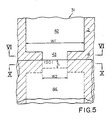
- the charge coupled device according to the present invention is similar to that shown in Fig. 1 with the exception of the configuration of each of the photo electric converting elements 31 to 33, and, for this reason, other elements, regions and films are designated by the same reference numerals used in Fig. 1 without any detailed description, and the heavily doped channel stopper 2 is indicated by hatch lines. All of the photo electric converting elements are identical with one another, so that description is made on the photo electric converting element 31 only with reference to Fig. 5.
- the photo electric converting element 31 has a generally rectangular wide portion 42 and a narrow portion 43 contiguous to the wide portion 43, and the narrow portion 43 extends below the transfer gate electrode 16 of the gate transistor 38.
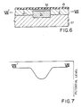
- the photo electric converting element 31 is implemented by an n-type impurity region 51 contacting a p-type impurity region 52 as similar to the prior art photo electric converting element (see Fig. 6)
- the p-type impurity region 52 is removed from the leading end sub-portion of the narrow portion 43 overlapped with the transfer gate electrode 16.
- a channel forming area 44 is defined by the channel stopper 2 and is contiguous to the leading end sub-portion of the narrow portion 43.
- the wide portion 42 is about 14 microns in width (W1), and the narrow portion 43 is as narrow as about 6 microns (W2).
- the overlapping area (S1) is as large as 28 square micron and, accordingly, results in 2.4 x 10³ residual electric charges.
- the narrow portion 43 is conducive to substantial reduction in the amount of the residual electric charges Qr, and any after image is less liable to take place on the display unit.
- the p-type channel stopper are formed on both sides of the n-type impurity region 51, and, for this reason, depletion layers extend from the p-n junctions between the n-type impurity region 51 and the p-type channel stopper 2 into the n-type impurity region 51. These depletion layers are causative of lifting the potential edge at the both side portions of the n-type impurity region 51 as shown in Fig. 7.
- Figs. 8(A) to 8(D) show a variety of channel configuration, and W is indicative of the width of an n-type impurity region 71.
- Reference numerals 72, 73 and 74 respectively designate a p-type channel stopper, an insulating film and a conductive film.
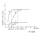
- the narrow portion 43 is of the structure shown in Fig. 8(C), and the potential level in terms of the width W traces Plots A of Fig. 9.
- the width is decreased to a value less than 6 microns, the potential level is lowered than that in the wide portion 42, and such a potential gap means a potential barrier between the wide portion 42 and the narrow portion 43 against the electric charges.
- the width W2 of the narrow portion 43 is of the order of 4 microns, the potential level thereof is about 1.3 volt, and, for this reason, the potential barrier of about 0.7 volt takes place between the wide portion 42 and the narrow portion 43.
- the narrow portion 43 needs to be equal to or greater than about 6 microns so as to avoid the potential barrier or the narrow channel phenomenon.
- the narrow portion 43 beneath the transfer gate electrode 16 is of the structure shown in Fig. 8(A), and the potential level in terms of the width W is represented by Plots B of Fig. 9. Namely, the leading sub-portion of the narrow portion 43 consists of the n-type impurity region 51 only as shown in Fig. 10.
- Plots B teaches us that potential level L2 at 6 microns is about 7.5 volts, so that the narrow channel phenomenon takes place in the width W of the order of 6 microns.
- the narrow portion 43 below the transfer gate electrode 16 merely allows the electric charge to pass therethrough, and the width W2 of the order of 6 micron is not causative of any problem because the potential level L2 is greater than the potential level L1 of 2 volts in the wide portion 42 (see Fig. 11).
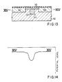
- a photo electric converting element 61 is fabricated on a semiconductor substrate 62 and defined by a p-type channel stopper 63 indicated by hatch lines.
- the photo electric converting element 61 is implemented by an n-type impurity region 64 partially covered with a p-type impurity region 65 as will be seen from Fig. 13, and the n-type impurity region 64 has a generally rectangular wide portion 66 and a narrow portion 67 projecting from the wide portion 66.
- the narrow portion 67 extends under a transfer gate electrode 68 of a gate transistor 69, so that a leading sub-portion of the narrow portion 67 is located under the transfer gate electrode 68, but a boss sub-portion is not overlain by the gate electrode 68.
- the gate transistor 69 provides a bridge between the photo electric converting element 61 and a vertical shift registor (not shown) as similar to the charge coupled device shown in Fig. 4, and the vertical shift registor in turn is coupled to a horizontal shift registor (not shown).
- the narrow portion 67 is not contiguous to the heavily doped channel stopper 63, but the lightly doped p-type semiconductor substrate 62 intervenes between the channel stopper 63 and the narrow portion 67.
- the photo electric converting element 61 thus arranged is of the structure shown in Fig. 8(D), and the potential level in terms of the width W varies along Plots C of Fig. 9. Comparing Plots A with Plots C, the narrow channel phenomenon is less liable to take place in the n-type impurity region 64 rather than the n-type impurity region 51. This is because of the fact that depletion layers easily extend into the lightly doped semiconductor substrate 62.
- the overlapping area S3 thus reduced results in the residual electric charges of about 3 x 10² which is a eighth of the residual electric charges produced in the prior art charge coupled device. As a result, any after image is effectively eliminated from a display unit.
- the residual electric charges are drastically reduced from the photo electric converting element according to the present invention without any serious problem in the nesting tolerance.
Abstract
Description
- This invention relates to a charge coupled device and, more particularly, to the configuration of a photo electric converting element.
- A solid state line sensor is implemented by a charge coupled device and used as an image sensor associated with an automatic focus controlling mechanism of a camera or incorporated in a facsimile machine.
- Fig. 1 shows the layout of a prior art charge coupled device fabricated on a p-type semiconductor substrate 1, and a p-
type channel stopper 2 provides an electrical isolation between adjacent photoelectric converting elements shift registor 5. The p-type channel stopper 2 is indicated by hatch lines for better understanding. As will be better seen from Fig. 2, each of the photo-electric converting elements electric converting element 4 is, by way of example, formed by an n-type impurity region 6 partially overlapped with a p-type impurity region 7. The n-type impurity region 6 is reversely biased with respect to the p-type semiconductor substrate 1. In the surface portion of the semiconductor substrate 1 is further formed an n-type impurity region 8 which forms theshift registor 5 together withtransfer gate electrodes insulating film 13 in a partially overlapping manner. Thetransfer gate electrodes transfer gate electrodes 11 and 12. Theshift registor 5 thus arranged transfers a data signal in the form of electric charges in synchronization with the two phase clock signal in the left direction of Fig. 1.Photo shield plates insulating film 13 and are spaced from each other for exposing a part of photo electric convertingelements electric converting element 4 is spaced apart form theshift registor 5, atransfer gate electrode 16 allows the electric charges to flow into theshift registor 5. Thetransfer gate electrode 16 is partially overlapped with the n-type impurity region 6 at a overlapping area L encircled bydash lines 17, and the edge of thetransfer gate electrode 9 extends below thetransfer gate electrode 16. Then, the electric charges accumulated in the n-type impurity region 6 are read out to theshift registor 5 in the presence of a transfer pulse Pt of a high voltage level fed to thetransfer gate electrode 16, and theshift registor 5 transfers the electric charges in synchronization with the two phase shift clock signal as described above. - However, a problem is encountered in the prior art charge coupled device in that residual electric charges Qr are left in the overlapping area L due to an undesirable potential well produced under the
transfer gate electrode 16 as shown in Fig. 3. Namely, when the transfer pulse Pt of the high voltage level is applied to thetransfer gate electrode 16, most of the electric charges flow into the n-type impurity region 8 under thetransfer gate electrode 9, however, the residual electric charges Qr are left in the potential well and gradually discharged into theshift registor 5 over a relatively large time constant. Thus, even though no effective electric charge is produced in the photo electric convertingelement 4, the residual electric charges Qr flow into theshift registor 5 in the presence of the transfer pulse Pt of the high voltage level, and are causative of an after image. - The residual electric charges may be reduced by decreasing the overlapping area to a certain extent allowed in consideration of a nesting tolerance. However, this approach never satisfies the user.
- It is therefore an important object of the present invention to provide a charge coupled device which completely transfers electric charges from photo electric converting elements to a shift registor.
- To accomplish the above object, the present invention proposes to decrease a leading end portion of an n-type impurity region in width to a certain extent preventing the n-type impurity region from a narrow channel phenomenon.
- In accordance with the present invention, there is provided a charge coupled device fabricated on a lightly doped semiconductor substrate of a first conductivity type, comprising: a) a plurality of photo electric converting elements implemented by a plurality of first impurity region of a second conductivity type formed in the semiconductor substrate and a plurality of second impurity regions of the first conductivity type respectively formed in the first impurity regions so as to form p-n junctions, respectively, the photo electric converting elements being formed into a plurality of element groups; b) a plurality of vertical shift registors respectively associated with the plurality of element groups and having third impurity regions of the second conductivity type, respectively; c) an insulating film covering the first, second and third impurity regions; and d) a plurality of gate transistors provided between the photo electric converting elements and the associated vertical shift registors, respectively, and having transfer gate electrodes respectively extending over channel forming areas between the first impurity regions and the third impurity regions, the first impurity regions being partially located under transfer gate electrodes, respectively, in which each of the first impurity regions comprises a wide portion and a narrow portion contiguous to the wide portion and having a boss sub-portion located in that area not overlapped with the transfer gate electrode and a leading end sub-portion overlapped with the transfer gate electrode, and in which the width of the boss sub-portion is greater than a critical value where a narrow channel phenomenon takes place.
- The features and advantages of a charge coupled device according to the present invention will be more clearly understood from the following description taken in conjunction with the accompanying drawings in which:
- Fig. 1 is a plan view showing the layout of a prior art charge coupled device;
- Fig. 2 is a cross sectional view taken along line II-II of Fig. 1 and showing the structure of the prior art charge coupled device;
- Fig. 3 is a diagram showing the potential profile produced in the prior art charge coupled device;
- Fig. 4 is a plan view showing the layout of an essential part of a charge coupled device embodying the present invention;
- Fig. 5 is a plan view showing a transfer gate between a photo electric converting element and a shift registor of the charge coupled device shown in Fig. 4;
- Fig. 6 is a cross sectional view taken along line VI-VI of Fig. 5 and showing the structure around a narrow portion of an n-type impurity region forming a part of the photo electric converting element;
- Fig. 7 is a graph showing the potential level along line VII-VII′ of Fig. 6;
- Figs. 8(A) to 8(D) are cross sectional views showing a variety of the structure of the narrow portion;
- Fig. 9 is a graph showing the potential level in terms of the width of the narrow portion;
- Fig. 10 is a cross sectional view taken along line X-X of Fig. 5 and showing the structure of the leading end sub-portion under the transfer gate electrode;
- Fig. 11 is a graph showing the potential level along line XI-XI of Fig. 10;
- Fig. 12 is a plan view showing the layout of a part of a photo electric converting element incorporated in another charge coupled device embodying the present invention;
- Fig. 13 is a cross sectional view taken along line XIII-XIII and showing the structure of a narrow portion of a photo electric converting region incorporated in the charge coupled device shown in Fig. 12;
- Fig. 14 is a graph showing the potential level along line XIV-XIV of Fig. 13;
- Fig. 15 is a cross sectional view taken along line XVI-XVI of Fig. 12 and showing the structure of the leading end bus-portion of the narrow portion; and
- Fig. 16 is a graph showing the potential level along line XVI-XVI of Fig. 15.
- Referring first to Fig. 4 of the drawings, a charge coupled device embodying the present invention largely comprises a photo array 30 having a plurality of photo electric converting
elements including elements registors including registors 34 and 35 and ahorizontal shift registor 36, and these components are fabricated on asingle semiconductor substrate 37. The photo electric converting elements are implemented by p-n junction type diodes, respectively. The photoelectric converting elements 31 to 33 are coupled to the associatedvertical shift registors 34 and 35 throughgate transistors vertical shift registors 34 and 35 are in turn coupled to ahorizontal shift registor 36. When an optical radiation carrying images is fallen upon the photoelectric converting elements 31 to 33, the photoelectric converting elements 31 to 33 produce electric charges depending upon the intensities of respective parts of the optical radiation, and the electric charges are transferred through the transfer gates to thevertical shift registors 34 and 35 in the presence of a transfer pulse Pt of an active high voltage level. The electric charges thus flowing into thevertical shift registors 34 and 35 are conveyed in synchronization with a two phase clock signal consisting of a first phase clock pulse CL1 and a second phase clock pulse CL2. The electric charges then flows into thehorizontal shift registor 36, and sequentially extracted from the horizontalshift regis tor 36. The electric charges thus sequentially extracted from thehorizontal shift registor 36 are used for reproducing the images on a display unit. The charge coupled device according to the present invention is similar to that shown in Fig. 1 with the exception of the configuration of each of the photo electric convertingelements 31 to 33, and, for this reason, other elements, regions and films are designated by the same reference numerals used in Fig. 1 without any detailed description, and the heavily dopedchannel stopper 2 is indicated by hatch lines. All of the photo electric converting elements are identical with one another, so that description is made on the photo electric convertingelement 31 only with reference to Fig. 5. - Turning to Fig. 5 of the drawings, the photo electric converting
element 31 has a generally rectangularwide portion 42 and anarrow portion 43 contiguous to thewide portion 43, and thenarrow portion 43 extends below thetransfer gate electrode 16 of the gate transistor 38. Although the photo electric convertingelement 31 is implemented by an n-type impurity region 51 contacting a p-type impurity region 52 as similar to the prior art photo electric converting element (see Fig. 6), the p-type impurity region 52 is removed from the leading end sub-portion of thenarrow portion 43 overlapped with thetransfer gate electrode 16. Achannel forming area 44 is defined by thechannel stopper 2 and is contiguous to the leading end sub-portion of thenarrow portion 43. In this instance, thewide portion 42 is about 14 microns in width (W1), and thenarrow portion 43 is as narrow as about 6 microns (W2). Assuming now that thenarrow portion 43 is overlapped with thetransfer gate electrode 16 by about 2 microns (L), the overlapping area S0 is calculated as L x W2 = 12 square microns, and 6 x 10² residual electric charges are actually measured in the overlapping area S0. If no narrow portion is formed below thetransfer gate electrode 16 as similar to the prior art charge coupled device, the overlapping area (S1) is as large as 28 square micron and, accordingly, results in 2.4 x 10³ residual electric charges. Thus, thenarrow portion 43 is conducive to substantial reduction in the amount of the residual electric charges Qr, and any after image is less liable to take place on the display unit. - The narrower the better in view of the reduction in the residual electric charges, however, if the width W2 is smaller than a critical value, undesirable narrow channel phenomenon takes place in the boundary area between the
wide portion 42 and thenarrow portion 43. As shown in Fig. 6, the p-type channel stopper are formed on both sides of the n-type impurity region 51, and, for this reason, depletion layers extend from the p-n junctions between the n-type impurity region 51 and the p-type channel stopper 2 into the n-type impurity region 51. These depletion layers are causative of lifting the potential edge at the both side portions of the n-type impurity region 51 as shown in Fig. 7. - In detail, Figs. 8(A) to 8(D) show a variety of channel configuration, and W is indicative of the width of an n-
type impurity region 71.Reference numerals narrow portion 43 is of the structure shown in Fig. 8(C), and the potential level in terms of the width W traces Plots A of Fig. 9. In this structure, if the width is decreased to a value less than 6 microns, the potential level is lowered than that in thewide portion 42, and such a potential gap means a potential barrier between thewide portion 42 and thenarrow portion 43 against the electric charges. In fact, if the width W2 of thenarrow portion 43 is of the order of 4 microns, the potential level thereof is about 1.3 volt, and, for this reason, the potential barrier of about 0.7 volt takes place between thewide portion 42 and thenarrow portion 43. Thus, thenarrow portion 43 needs to be equal to or greater than about 6 microns so as to avoid the potential barrier or the narrow channel phenomenon. Thenarrow portion 43 beneath thetransfer gate electrode 16 is of the structure shown in Fig. 8(A), and the potential level in terms of the width W is represented by Plots B of Fig. 9. Namely, the leading sub-portion of thenarrow portion 43 consists of the n-type impurity region 51 only as shown in Fig. 10. Plots B teaches us that potential level L2 at 6 microns is about 7.5 volts, so that the narrow channel phenomenon takes place in the width W of the order of 6 microns. However, thenarrow portion 43 below thetransfer gate electrode 16 merely allows the electric charge to pass therethrough, and the width W2 of the order of 6 micron is not causative of any problem because the potential level L2 is greater than the potential level L1 of 2 volts in the wide portion 42 (see Fig. 11). - Turning to Fig. 12 of the drawings, a photo
electric converting element 61 is fabricated on asemiconductor substrate 62 and defined by a p-type channel stopper 63 indicated by hatch lines. The photoelectric converting element 61 is implemented by an n-type impurity region 64 partially covered with a p-type impurity region 65 as will be seen from Fig. 13, and the n-type impurity region 64 has a generally rectangularwide portion 66 and a narrow portion 67 projecting from thewide portion 66. The narrow portion 67 extends under atransfer gate electrode 68 of a gate transistor 69, so that a leading sub-portion of the narrow portion 67 is located under thetransfer gate electrode 68, but a boss sub-portion is not overlain by thegate electrode 68. Though not shown in the drawings, the gate transistor 69 provides a bridge between the photoelectric converting element 61 and a vertical shift registor (not shown) as similar to the charge coupled device shown in Fig. 4, and the vertical shift registor in turn is coupled to a horizontal shift registor (not shown). - As will be better seen from Fig. 13, the narrow portion 67 is not contiguous to the heavily doped
channel stopper 63, but the lightly doped p-type semiconductor substrate 62 intervenes between thechannel stopper 63 and the narrow portion 67. The photoelectric converting element 61 thus arranged is of the structure shown in Fig. 8(D), and the potential level in terms of the width W varies along Plots C of Fig. 9. Comparing Plots A with Plots C, the narrow channel phenomenon is less liable to take place in the n-type impurity region 64 rather than the n-type impurity region 51. This is because of the fact that depletion layers easily extend into the lightly dopedsemiconductor substrate 62. In fact, no narrow channel phenomenon takes place in so far as the width of the narrow portion 67 is not less than about 3 microns. At the leading sub-portion, the narrow channel phenomenon takes place, but the potential level is much larger than about 2 volts in thewide portion 66, so that the leading end sub-portion provides a conduction path which allows the electric charges to smoothly flow into the vertical shift registor as shown in Fig. 16. - By virtue of the narrow portion 67 contiguous to the lightly doped
semiconductor substrate 62, the narrow portion 67 is decreased in width W4 to about 3 microns, and an overlapping area S3 is given as W4 x L = 6 square micron. The overlapping area S3 thus reduced results in the residual electric charges of about 3 x 10² which is a eighth of the residual electric charges produced in the prior art charge coupled device. As a result, any after image is effectively eliminated from a display unit. - As will be understood from the foregoing description, the residual electric charges are drastically reduced from the photo electric converting element according to the present invention without any serious problem in the nesting tolerance.
- Although particular embodiments of the present invention have been shown and described, it will be obvious to those skilled in the art that various changes and modifications may be made without departing from the spirit and scope of the present invention.
Claims (1)
Applications Claiming Priority (2)
| Application Number | Priority Date | Filing Date | Title |
|---|---|---|---|
| JP40770/89 | 1989-02-20 | ||
| JP1040770A JPH02219270A (en) | 1989-02-20 | 1989-02-20 | Solid-state image pickup device |
Publications (2)
| Publication Number | Publication Date |
|---|---|
| EP0384286A1 true EP0384286A1 (en) | 1990-08-29 |
| EP0384286B1 EP0384286B1 (en) | 1994-05-11 |
Family
ID=12589869
Family Applications (1)
| Application Number | Title | Priority Date | Filing Date |
|---|---|---|---|
| EP90102894A Expired - Lifetime EP0384286B1 (en) | 1989-02-20 | 1990-02-14 | Charge coupled device free from after image due to residual electric charges |
Country Status (4)
| Country | Link |
|---|---|
| US (1) | US5049960A (en) |
| EP (1) | EP0384286B1 (en) |
| JP (1) | JPH02219270A (en) |
| DE (1) | DE69008749T2 (en) |
Cited By (2)
| Publication number | Priority date | Publication date | Assignee | Title |
|---|---|---|---|---|
| US5189498A (en) * | 1989-11-06 | 1993-02-23 | Mitsubishi Denki Kabushiki Kaisha | Charge coupled device |
| US5302543A (en) * | 1989-11-06 | 1994-04-12 | Mitsubishi Denki Kabushiki Kaisha | Method of making a charge coupled device |
Families Citing this family (4)
| Publication number | Priority date | Publication date | Assignee | Title |
|---|---|---|---|---|
| JP3125303B2 (en) * | 1990-11-26 | 2001-01-15 | 日本電気株式会社 | Solid-state imaging device |
| JP3297988B2 (en) * | 1997-01-24 | 2002-07-02 | シャープ株式会社 | Active matrix substrate |
| US6476426B1 (en) | 1999-07-06 | 2002-11-05 | Motorola, Inc. | Electronic component and method for improving pixel charge transfer in the electronic component |
| DE102007029898B3 (en) * | 2007-06-28 | 2008-08-21 | MAX-PLANCK-Gesellschaft zur Förderung der Wissenschaften e.V. | Semiconductor detector, particularly pn charged coupled device detector, for radiation detection, has guard ring, selection anode arranged within guard ring for reading out radiation |
Citations (4)
| Publication number | Priority date | Publication date | Assignee | Title |
|---|---|---|---|---|
| DE2527597B2 (en) * | 1975-06-20 | 1977-04-14 | Siemens AG, 1000 Berlin und 8000 München | ONE-DIMENSIONAL OPTOELECTRONIC SCANNING DEVICE |
| DE2542156B2 (en) * | 1975-09-22 | 1977-12-08 | Siemens AG, 1000 Berlin und 8000 München | ONE DIMENSIONAL OPTOELECTRONIC SENSOR |
| US4087833A (en) * | 1977-01-03 | 1978-05-02 | Reticon Corporation | Interlaced photodiode array employing analog shift registers |
| US4236168A (en) * | 1978-03-28 | 1980-11-25 | Siemens Aktiengesellschaft | One-dimensional CCD sensor with overflow arrangement |
Family Cites Families (6)
| Publication number | Priority date | Publication date | Assignee | Title |
|---|---|---|---|---|
| GB1437328A (en) * | 1972-09-25 | 1976-05-26 | Rca Corp | Sensors having recycling means |
| JPS6033345B2 (en) * | 1979-06-08 | 1985-08-02 | 日本電気株式会社 | Charge transfer imaging device and its driving method |
| US4484210A (en) * | 1980-09-05 | 1984-11-20 | Nippon Electric Co., Ltd. | Solid-state imaging device having a reduced image lag |
| US4696021A (en) * | 1982-06-03 | 1987-09-22 | Nippon Kogaku K.K. | Solid-state area imaging device having interline transfer CCD means |
| JPS60202961A (en) * | 1984-03-28 | 1985-10-14 | Hitachi Ltd | Charge transfer type solid state image sensor element |
| JPH0682823B2 (en) * | 1984-06-27 | 1994-10-19 | 株式会社東芝 | Solid-state imaging device |
-
1989
- 1989-02-20 JP JP1040770A patent/JPH02219270A/en active Pending
-
1990
- 1990-02-14 EP EP90102894A patent/EP0384286B1/en not_active Expired - Lifetime
- 1990-02-14 DE DE69008749T patent/DE69008749T2/en not_active Expired - Fee Related
- 1990-02-20 US US07/482,096 patent/US5049960A/en not_active Expired - Lifetime
Patent Citations (4)
| Publication number | Priority date | Publication date | Assignee | Title |
|---|---|---|---|---|
| DE2527597B2 (en) * | 1975-06-20 | 1977-04-14 | Siemens AG, 1000 Berlin und 8000 München | ONE-DIMENSIONAL OPTOELECTRONIC SCANNING DEVICE |
| DE2542156B2 (en) * | 1975-09-22 | 1977-12-08 | Siemens AG, 1000 Berlin und 8000 München | ONE DIMENSIONAL OPTOELECTRONIC SENSOR |
| US4087833A (en) * | 1977-01-03 | 1978-05-02 | Reticon Corporation | Interlaced photodiode array employing analog shift registers |
| US4236168A (en) * | 1978-03-28 | 1980-11-25 | Siemens Aktiengesellschaft | One-dimensional CCD sensor with overflow arrangement |
Cited By (2)
| Publication number | Priority date | Publication date | Assignee | Title |
|---|---|---|---|---|
| US5189498A (en) * | 1989-11-06 | 1993-02-23 | Mitsubishi Denki Kabushiki Kaisha | Charge coupled device |
| US5302543A (en) * | 1989-11-06 | 1994-04-12 | Mitsubishi Denki Kabushiki Kaisha | Method of making a charge coupled device |
Also Published As
| Publication number | Publication date |
|---|---|
| JPH02219270A (en) | 1990-08-31 |
| EP0384286B1 (en) | 1994-05-11 |
| DE69008749D1 (en) | 1994-06-16 |
| DE69008749T2 (en) | 1994-08-25 |
| US5049960A (en) | 1991-09-17 |
Similar Documents
| Publication | Publication Date | Title |
|---|---|---|
| US4373167A (en) | Solid state image sensor with overflow protection and high resolution | |
| US4517733A (en) | Process for fabricating thin film image pick-up element | |
| US5517043A (en) | Split pixel interline transfer imaging device | |
| EP0403279A1 (en) | High voltage thin film transistor with second gate | |
| US4236168A (en) | One-dimensional CCD sensor with overflow arrangement | |
| US4471371A (en) | Thin film image pickup element | |
| JPS5928110B2 (en) | Infrared image sensor circuit layout | |
| US5256890A (en) | Non-interlacing charge coupled device of a frame interline transfer type | |
| EP0384286A1 (en) | Charge coupled device free from after image due to residual electric charges | |
| US4884143A (en) | Lamination type solid image pick up apparatus for avoiding a narrow channel effect | |
| US6242769B1 (en) | Thin film transistor type photo sensor | |
| US5196719A (en) | Solid-state image pick-up device having electric field for accelerating electric charges from photoelectric converting region to shift register | |
| KR100525044B1 (en) | Method for fabricating the thin film transistor type photo sensor | |
| US20020040997A1 (en) | Semiconductor device | |
| US5289029A (en) | Semiconductor integrated circuit device having wells biased with different voltage levels | |
| JPH03256359A (en) | Solid state imager | |
| US5294817A (en) | Output circuit for charged transfer device and having a high detection sensitivity | |
| EP0457192B1 (en) | Solid-state image pick-up device having electric field for accelerating electric charges from photo-electric converting region to shift register | |
| US5336910A (en) | Charge coupled device of high sensitivity and high integration | |
| EP0457271B1 (en) | A charge transfer device | |
| JPS6134263B2 (en) | ||
| JPS60227467A (en) | Image sensor | |
| US5337474A (en) | Process for fabricating electronic devices and image sensor | |
| US7514687B2 (en) | Energy ray detecting element | |
| US6310933B1 (en) | Charge transferring device and charge transferring method which can reduce floating diffusion capacitance |
Legal Events
| Date | Code | Title | Description |
|---|---|---|---|
| PUAI | Public reference made under article 153(3) epc to a published international application that has entered the european phase |
Free format text: ORIGINAL CODE: 0009012 |
|
| 17P | Request for examination filed |
Effective date: 19900214 |
|
| AK | Designated contracting states |
Kind code of ref document: A1 Designated state(s): DE FR GB |
|
| 17Q | First examination report despatched |
Effective date: 19930914 |
|
| GRAA | (expected) grant |
Free format text: ORIGINAL CODE: 0009210 |
|
| AK | Designated contracting states |
Kind code of ref document: B1 Designated state(s): DE FR GB |
|
| PG25 | Lapsed in a contracting state [announced via postgrant information from national office to epo] |
Ref country code: FR Effective date: 19940511 |
|
| REF | Corresponds to: |
Ref document number: 69008749 Country of ref document: DE Date of ref document: 19940616 |
|
| EN | Fr: translation not filed | ||
| PLBE | No opposition filed within time limit |
Free format text: ORIGINAL CODE: 0009261 |
|
| STAA | Information on the status of an ep patent application or granted ep patent |
Free format text: STATUS: NO OPPOSITION FILED WITHIN TIME LIMIT |
|
| 26N | No opposition filed | ||
| REG | Reference to a national code |
Ref country code: GB Ref legal event code: IF02 |
|
| PGFP | Annual fee paid to national office [announced via postgrant information from national office to epo] |
Ref country code: GB Payment date: 20030212 Year of fee payment: 14 |
|
| PGFP | Annual fee paid to national office [announced via postgrant information from national office to epo] |
Ref country code: DE Payment date: 20030227 Year of fee payment: 14 |
|
| REG | Reference to a national code |
Ref country code: GB Ref legal event code: 732E |
|
| PG25 | Lapsed in a contracting state [announced via postgrant information from national office to epo] |
Ref country code: GB Free format text: LAPSE BECAUSE OF NON-PAYMENT OF DUE FEES Effective date: 20040214 |
|
| PG25 | Lapsed in a contracting state [announced via postgrant information from national office to epo] |
Ref country code: DE Free format text: LAPSE BECAUSE OF NON-PAYMENT OF DUE FEES Effective date: 20040901 |
|
| GBPC | Gb: european patent ceased through non-payment of renewal fee |
Effective date: 20040214 |