EP0384207A2 - Method of allocating digital signals to parallel receiving channels - Google Patents
Method of allocating digital signals to parallel receiving channels Download PDFInfo
- Publication number
- EP0384207A2 EP0384207A2 EP19900102281 EP90102281A EP0384207A2 EP 0384207 A2 EP0384207 A2 EP 0384207A2 EP 19900102281 EP19900102281 EP 19900102281 EP 90102281 A EP90102281 A EP 90102281A EP 0384207 A2 EP0384207 A2 EP 0384207A2
- Authority
- EP
- European Patent Office
- Prior art keywords
- digital signals
- frame
- signal
- word
- time
- Prior art date
- Legal status (The legal status is an assumption and is not a legal conclusion. Google has not performed a legal analysis and makes no representation as to the accuracy of the status listed.)
- Withdrawn
Links
Images

Classifications
-
- H—ELECTRICITY
- H04—ELECTRIC COMMUNICATION TECHNIQUE
- H04J—MULTIPLEX COMMUNICATION
- H04J3/00—Time-division multiplex systems
- H04J3/02—Details
- H04J3/06—Synchronising arrangements
- H04J3/0602—Systems characterised by the synchronising information used
- H04J3/0605—Special codes used as synchronising signal
- H04J3/0608—Detectors therefor, e.g. correlators, state machines
Definitions
- the invention relates to a method according to the preamble of patent claim 1.
- Each digital signal can itself be a time-division multiplex signal, which is then combined with other such digital signals to form a time-division multiplex digital signal of a higher order. For example, four digital signals with a bit rate of 140 Mbit / s combined into a time-division multiplexed digital signal with a bit rate of 565 Mbit / s.
- a demultiplexer provides the original digital signals again by dissolving this time-division multiplexed digital signal, these must be distributed in parallel on the correct reception channels.
- the distribution by the demultiplexer is random. There are as many options as there are digital signals, four options with four digital signals.
- a method according to the preamble of claim 1 is used to produce the correct assignment.
- An arrangement for carrying out this method is supplied with a clock signal and four digital signals via four parallel channels, the digital signals coming from a demultiplexer being synchronized and reaching a channel distributor.
- the four digital signals are also fed to a circuit for recognizing the frame identification word of the time-division multiplexed digital signal, which circuit synchronizes a frame counter due to the beginning of the frame identification word.
- FIG. 1 shows a channel distributor 1 which contains a register 15, a counter 16, a divider 17 and four selector switches 11 to 14.
- Switches 11 to 14 are referred to as selector switches because they optionally connect one of several inputs to their output.
- the channel distributor 1 is supplied by a demultiplexer (which is not part of the invention and is not shown in FIG. 1) four digital signals 1, 2, 3, 4 via four individual channels K1 to K4 and separately via a channel K5, a clock signal, this has the same bit rate as digital signals 1 to 4.
- the digital signals 1 to 4 each contain a fourth bit in a cyclic sequence in the case of a time-divisionally multiplexed signal.
- the number of bits of the frame identification word is chosen as an integer multiple of the number of digital signals at a bit repetition rate of 565 Mbit / s.
- the CCITT recommendations G.922 or G.954 it has the bit sequence 111110100000, of which three bits are assigned to each digital signal 1 to 4, with only the assignment A, synchronous to the bit rate of the time-division multiplex signal, within three bit cycles of the bit rate of the Digital signals 1 to 4 occur.
- the other assignments B, C, D any other bits X in channels K1 to K4 are transmitted simultaneously with bits from the frame identifier.
- the digital signals 1 to 4 are delayed by one bit via the register 15 clocked by the clock signal with outputs R1 to R4; the outputs R1 to R4 are assigned to the channels K1 to K4 in sequence: at the outputs R1 to R4 there are the following during the sequence of four bits 0, 1, 2, 3, with bit 0 preceding bit 1 , combinations shown in diagram 3 in the digital signals.
- the channels K1, K2, K3 are directly connected to the inputs of the selector switches 12 to 14, which are channels K1 to K4 indirectly connected via register 15 to the inputs of selector switches 11 to 14.
- the selector switches 11 to 14 each have four inputs, between which cyclically with the periodicity of at least one pulse frame, but preferably two, generally m pulse frames, where m is a natural number, is switched by means of the counter 16, and are sequential over one output each connected to a receiving channel E1 to E4.
- output assignments A ′, B ′, C ′, D ′ are generated so that within the duration of a number of pulse frames proportional to the number of parallel digital signals, the correct output assignment A ′ by means of a transformation A ⁇ A ′, B ⁇ A ′, C ⁇ A ′, D ⁇ A ′ effected by means of the selector switches 11-14, with the reception channels E1 to E4 according to diagram 4 in the assignments A to D.
- the divider 16 has switched the selector switches 11 to 14 in this assignment A ', in which the frame identification word occurs "synchronously" within a period of 3 bits on the receiving channels, it can be detected by means of a circuit 2.
- a channel distributor 1 contains n selector switches for n parallel digital signals, which switch into n positions, where n is a natural number. Of the n digital signals, the selector switch n-1 is delayed and all n are supplied without delay.
- n transformations are possible for a period of at least n pulse frames, but preferably 2n pulse frames, among which one is certainly the correct one, on the basis of which the frame identifier can be recognized in circuit 2.
- the circuit 2 contains three AND gates 21, 23, 25 and two D flip-flops 22, 24 clocked by the clock signal via channel K5.
- the four non-inverting inputs of the AND gate 21 are each with the receiving channels E1 to E4 connected.
- the bit combination 1111 which occurs first in parallel in the receive channels, generates a "1" signal at the output of the AND gate 21, which is fed to the D flip-flop 22 and stored there for the duration of one bit.
- the AND gate 23 has three non-inverting inputs, one of which is connected to the receiving channel E1, a second to the receiving channel E3 and the third to the output of the D flip-flop 22.
- One of the two inverting inputs is connected to the receiving channel E2, the other to the receiving channel E4.
- the AND gate 23 If the bit combination 1010 occurs immediately after the bit combination, the AND gate 23 generates at its output a "1" signal which is fed to the D flip-flop 24 and stored there for the duration of a bit. Then it gets into the AND gate 25 via its non-inverting input.
- the AND gate 25 also has four inverting inputs, each of which is connected to the receiving channels E1 to E4.
- the AND gate 25 forms a "1" signal which means "frame identifier word recognized”.
- a circuit 2 for recognizing a frame identification word contains logic circuits such as AND, OR, NOR and NAND gates and delay registers in order to be able to detect temporal sequences as a whole.
- the "1" signal is fed to a synchronizer 3, which in turn is controlled by a frame counter 4.
- the frame counter 4 is clocked by the clock signal via the channel K5 and generates a pulse frame of a predetermined length; at a bit repetition frequency of 140 Mbit / s according to CCITT recommendation G. 922, a pulse frame with a length of 672 bits, corresponding to a pulse frame of the same duration with 2688 bits in the time-division multiplexed digital signal.
- the pulse frame generated by the frame counter 4 is generally not synchronized with the pulse frame of the time-division multiplexed digital signal.
- the frame counter 4 therefore has an input 41 via which it is set in synchronism with the pulse frame of the time-division multiplexed digital signal when the synchronizer 3 reaches synchronism.
- the frame counter 4 outputs signals S1 to S3 to the synchronizer 3 via its outputs 42 to 44 at certain times within the pulse frame it generates.
- the synchronizer 3 consists of two counters 33, 34, two AND gates 31, 32 and an RS flip-flop 35.
- the frame counter 4 clocks the divider 17 of the channel distributor 1 once with the signal S3 during the frame it generates.
- the divider 17 switches after preferably every second frame of the frame counter 3 and gives the counter 16 a signal so that it counts up by 1.
- the counter 16 counts up to the number that corresponds to the number of channels (here: 4), that is to say it starts from the beginning every 8 frames.
- the divider 17 therefore switches over after every second frame generated by the frame counter 4, so that the frame identification word in the circuit 2 can still be recognized with certainty even if it occurs at the point in time at which the counter 16 continues to count.
- the divider 17 switches and the counter 16 continues to count until a frame identifier is recognized.
- the frame counter 4 is set via its input 41 in synchronism with the received frame.
- the signal S3 which also briefly assumes the state "0" during the duration of the pulse frame generated by the frame counter 4, preceding the signal S1, is fed to the clock inputs of the counters 33 and 34.
- the circuit 2 If, while the signal S3 assumes the state "0", the circuit 2 outputs the signal "frame identifier word recognized", the counter 33 counts up by 1, the counter 34 is set to zero. If, however, no frame identifier word has been detected, the counter 34 counts up by 1 and the counter 33 is set to zero.
- the counter 33 When the counter 33 has reached the counter reading 3, it sets the RS flip-flop 35 via its first output. This remains set until it is reset after four times the frame identification word has not been recognized, on the basis of which the counter 34 to 4 has counted becomes. Its Q output, when set, indicates that the device is running synchronously.
- This information can be used for alarm purposes.
- a frame ID must have been found three times in succession so that - according to the CCITT recommendations - the frame synchronism is considered to be achieved, which is then considered lost if a frame ID was not recognized four times in succession.
- a synchronization circuit according to the invention generally only has to meet the criterion that, on reaching the synchronism, it sets the frame counter 3 to zero on the one hand and suppresses clock pulses from the frame counter to the divider 17.
- Other connections of gates, counters and flip-flops are also suitable for this.
- the RS flip-flop 35 may have an undefined state at the time the synchronizer starts operating, it can also be replaced by a JK flip-flop.
- runtime delays can occur within the arrangement shown in FIG. 1, which can be compensated for by inserting delaying components at other points.
- the circuit 2 may have to be modified depending on the type and duration of the frame code word.
Landscapes
- Engineering & Computer Science (AREA)
- Computer Networks & Wireless Communication (AREA)
- Signal Processing (AREA)
- Time-Division Multiplex Systems (AREA)
Abstract
Description
Die Erfindung betrifft ein Verfahren nach dem Oberbegriff des Patentanspruchs 1.The invention relates to a method according to the preamble of
Es gibt Verfahren für die digitale Nachrichtenübertragung, in denen sendeseitig Digitalsignale aus verschiedenen Kanälen wortweise oder bitweise zu einem Zeitmultiplexsignal zusammengefaßt werden. Dabei kann jedes Digitalsignal selbst schon ein Zeitmultiplexsignal sein, das dann mit anderen solchen Digitalsignalen zu einem Zeitmultiplex-Digitalsignal höherer Ordnung zusammengefaßt wird. So werden z.B. vier Digitalsignale mit einer Bitfolgefrequenz von 140 Mbit/s zu einem Zeitmultiplex-Digitalsignal mit einer Bitfolgefrequenz von 565 Mbit/s zusammengefaßt.There are methods for digital message transmission in which digital signals from different channels are combined word by word or bit by bit to form a time-division multiplex signal. Each digital signal can itself be a time-division multiplex signal, which is then combined with other such digital signals to form a time-division multiplex digital signal of a higher order. For example, four digital signals with a bit rate of 140 Mbit / s combined into a time-division multiplexed digital signal with a bit rate of 565 Mbit / s.
Wenn ein Demultiplexer durch Auflösen dieses Zeitmultiplex-Digitalsignals wieder die ursprünglichen Digitalsignale bereitstellt, müssen diese auf den richtigen Empfangskanälen parallel verteilt werden. Die Verteilung durch den Demultiplexer ist zufällig. Es gibt soviele Möglichkeiten, wie es Digitalsignale gibt, bei vier Digitalsignalen also vier Möglichkeiten.If a demultiplexer provides the original digital signals again by dissolving this time-division multiplexed digital signal, these must be distributed in parallel on the correct reception channels. The distribution by the demultiplexer is random. There are as many options as there are digital signals, four options with four digital signals.
Zur Herstellung der richtigen Zuordnung dient ein Verfahren nach dem Oberbegriff des Patentanspruchs 1.A method according to the preamble of
Aus der "Nachrichtentechnischen Zeitschrift", (ntz), S. 16 ff., 36 (1983), ist ein solches Verfahren bekannt.Such a method is known from the "Nachrichtenentechnische Zeitschrift", (ntz), p. 16 ff., 36 (1983).
Einer Anordnung zur Durchführung dieses Verfahrens werden ein Taktsignal und über vier parallele Kanäle vier Digitalsignale zugeführt, wobei die Digitalsignale, aus einem Demultiplexer kommend, synchronisiert werden und zu einem Kanalverteiler gelangen.An arrangement for carrying out this method is supplied with a clock signal and four digital signals via four parallel channels, the digital signals coming from a demultiplexer being synchronized and reaching a channel distributor.
Die vier Digitalsignale werden außerdem einer Schaltung zur Erkennung des Rahmenkennungswortes des Zeitmultiplex-Digitalsignals zugeführt, die aufgrund des Beginns des Rahmenkennungswortes einen Rahmenzähler synchronisiert.The four digital signals are also fed to a circuit for recognizing the frame identification word of the time-division multiplexed digital signal, which circuit synchronizes a frame counter due to the beginning of the frame identification word.
Einzelheiten zu den in der Schrift gezeigten Baugruppen sind nicht erwähnt.Details of the assemblies shown in the document are not mentioned.
Es ist die Aufgabe der Erfindung, ein Verfahren der eingangs genannten Art zu schaffen, das mit anderen als den bekannten Mitteln die Zuordnung der Digitalsignale auf Empfangskanäle erreicht.It is the object of the invention to provide a method of the type mentioned at the outset which achieves the assignment of the digital signals to reception channels using means other than the known means.
Die Aufgabe wird gelöst, wie in Patentanspruch 1 angegeben. Weiterbildungen ergeben sich aus den Unteransprüchen.The object is achieved as stated in
Die Erfindung wird anhand der Figuren beispielsweise erläutert. Es zeigen:
- Fig. 1 ein Schaltbild einer erfindungsgemäßen Vorrichtung, bestehend aus einem Kanalverteiler, einem Rahmenzähler, einer Schaltung zur Erkennung des Rahmenkennungswortes und einem Synchronisierer;
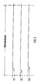
- Fig. 2 ein Impulsdiagramm, das die Wirkungsweise des Rahmenzählers erläutert.
- 1 shows a circuit diagram of a device according to the invention, consisting of a channel distributor, a frame counter, a circuit for recognizing the frame identifier and a synchronizer;
- Fig. 2 is a timing diagram that explains the operation of the frame counter.
Fig. 1 zeigt einen Kanalverteiler 1, der ein Register 15, einen Zähler 16, einen Teiler 17 und vier Wählschalter 11 bis 14 enthält.1 shows a
Als Wählschalter werden die Schalter 11 bis 14 deshalb bezeichnet, weil sie wahlweise einen von mehreren Eingängen mit ihrem Ausgang verbinden.Switches 11 to 14 are referred to as selector switches because they optionally connect one of several inputs to their output.
Im vorliegenden Fall schalten sie zyklisch. Dem Kanalverteiler 1 werden von einem Demultiplexer (der nicht Teil der Erfindung und in Fig. 1 nicht dargestellt ist) vier Digitalsignale 1, 2, 3, 4 über vier einzelne Kanäle K1 bis K4 und gesondert über einen Kanal K5 ein Taktsignal zugeführt, wobei dieses die gleiche Bitfolgefrequenz wie die Digitalsignale 1 bis 4 hat.In the present case, they switch cyclically. The
Da die Aufteilung der Digitalsignale auf die Kanäle K1 bis K4 rein zufällig ist, ergeben sich duch zyklische Vertauschung vier Zuordnungen A, B, C, D der Digitalsignale 1 bis 4 auf die Kanäle K1 bis K4, dargestellt in Diagramm 1.
Entsprechend enthalten die Digitalsignale 1 bis 4 bei einem bitweise aufgelösten Zeitmultiplexsignal ein jeweils viertes Bit in zyklischer Folge. Die Anzahl der Bits des Rahmenkennungsworts ist in diesem Fall bei einer Bitfolgefrequenz von 565 Mbit/s als ganzzahliges Vielfaches der Anzahl der Digitalsignale gewählt.Correspondingly, the
Nach den CCITT-Empfehlungen G.922 oder G.954 hat es die Bitsequenz 111110100000, von der entsprechend jedem Digitalsignal 1 bis 4 drei Bits zugeordnet werden, wobei nur die Zuordnung A, synchron zur Bitfolgefrequenz des Zeitmultiplexsignals, innerhalb von drei Bittakten der Bitfolgefrequenz der Digitalsignale 1 bis 4 erfolgt. Bei den anderen Zuordnungen B, C, D werden zeitgleich mit Bits aus dem Rahmenkennungswort beliebige andere Bits X in den Kanälen K1 bis K4 übertragen.According to the CCITT recommendations G.922 or G.954, it has the bit sequence 111110100000, of which three bits are assigned to each
Dies ist in Diagramm 2 dargestellt.This is shown in diagram 2.
Am Eingang des Kanalverteilers 1 sind daher während einer vier Bits 1, 2, 3, 4 entsprechenden Zeitdauer, in der Bits aus dem Rahmenkennungswort auftreten, folgende Kombinationen der Digitalsignale 1 bis 4 möglich:
Die Digitalsignale 1 bis 4 werden über das durch das Taktsignal getaktete Register 15 mit Ausgängen R1 bis R4 um ein Bit verzögert; die Ausgänge R1 bis R4 sind der Reihe nach den Kanälen K1 bis K4 zugeordnet: an den Ausgängen R1 bis R4 liegen während der Folge von vier Bits 0, 1, 2, 3, - wobei das Bit 0 zeitlich dem Bit 1 vorausgeht - ,folgende, im Diagramm 3 gezeigte Kombinationen in den Digitalsignalen vor.The
Zur Vereinfachung werden die Digitalsignale hier mit den Ausgängen R1 bis R4 bezeichnet, an denen sie auftreten.
Die Kanäle K1, K2, K3 sind unmittelbar mit den Eingängen der Wählschalter 12 bis 14, die Kanäle K1 bis K4 sind mittelbar über das Register 15 mit den Eingängen der Wählschalter 11 bis 14 verbunden.The channels K1, K2, K3 are directly connected to the inputs of the
Die Wählschalter 11 bis 14 haben jeweils vier Eingänge, zwischen denen zyklisch mit der Periodizität von mindestens einem Pulsrahmen, vorzugsweise jedoch zwei, im allgemeinen m Pulsrahmen, wobei m eine natürliche Zahl ist, mittels des Zählers 16 geschaltet wird, und sind der Reihe nach über jeweils einen Ausgang mit jeweils einem Empfangskanal E1 bis E4 verbunden.The selector switches 11 to 14 each have four inputs, between which cyclically with the periodicity of at least one pulse frame, but preferably two, generally m pulse frames, where m is a natural number, is switched by means of the
Zwischen den insgesamt 16 Eingängen der Wählschalter wird in vier Stellungen derart geschaltet, daß aus jeder der eingangsseitigen Zuordnungen A bis D, wie sie die Digitalsignale, die auf den Kanälen K1, K2, K3 unverzögert, oder von den Ausgängen des Registers 15, R1 bis R4, kommend, um ein Bit verzögert, zusammen darstellen, ausgangsseitige Zuordnungen A′, B′, C′, D′ erzeugt werden, so daß innerhalb der Dauer einer zur Anzahl der zueinander parallelen Digitalsignale proportionalen Anzahl von Pulsrahmen die richtige ausgangsseitige Zuordnung A′ durch eine mittels der Wählschalter 11-14 bewirkte Transformation A → A′, B → A′, C → A′, D → A′ mit Sicherheit erreicht wird, indem die Empfangskanäle E1 bis E4 gemäß Diagramm 4 bei den Zuordnungen A bis D auf die folgende Weise geschaltet werden:
Wenn der Teiler 16 die Wählschalter 11 bis 14 in diese Zuordnung A′ geschaltet hat, in der auf den Empfangskanälen das Rahmenkennungswort innerhalb einer Zeitdauer von 3 Bits "synchron" auftritt, kann es mittels einer Schaltung 2 detektiert werden.If the
Allgemein enthält ein erfindungsgemäßer Kanalverteiler 1 bei n zueinander parallelen Digitalsignalen n Wählschalter, die in n Stellungen schalten, wobei n eine natürliche Zahl ist. Von den n Digitalsignalen werden dem Wählschalter n-1 verzögert und alle n unverzögert zugeführt.In general, a
Mittels der Wählschalter sind während einer Dauer von mindestens n Pulsrahmen, vorzugsweise jedoch 2n Pulsrahmen, n Transformationen möglich, unter denen eine mit Sicherheit die richtige ist, aufgrund deren in der Schaltung 2 das Rahmenkennungswort erkannt werden kann.By means of the selector switches, n transformations are possible for a period of at least n pulse frames, but preferably 2n pulse frames, among which one is certainly the correct one, on the basis of which the frame identifier can be recognized in
Die Schaltung 2 enthält drei UND-Gatter 21, 23, 25 und zwei durch das Taktsignal über Kanal K5 getaktete D-Flip-Flops 22, 24. Die vier nicht-invertierenden Eingänge des UND-Gatters 21 sind jeweils mit den Empfangskanälen E1 bis E4 verbunden. Die Bitkombination 1111, die als erste parallel in den Empfangskanälen auftritt, erzeugt ein "1"-Signal am Ausgang des UND-Gatters 21, das dem D-Flip-Flop 22 zugeführt und dort für die Zeitdauer eines Bits gespeichert wird. Das UND-Gatter 23 hat drei nicht-invertierende Eingänge, von denen einer mit dem Empfangskanal E1, ein zweiter mit dem Empfangskanal E3 und der dritte mit dem Ausgang des D-Flip-Flops 22 verbunden ist.The
Von den beiden invertierenden Eingängen ist der eine mit dem Empfangskanal E2, der andere mit dem Empfangskanal E4 verbunden.One of the two inverting inputs is connected to the receiving channel E2, the other to the receiving channel E4.
Sofern die Bitkombination 1010 sofort nach der Bitkombination auftritt, erzeugt das UND-Gatter 23 an seinem Ausgang ein "1"-Signal, das dem D-Flip-Flop 24 zugeführt und dort für die Zeitdauer eines Bits gespeichert wird. Dann gelangt es in das UND-Gatter 25 über dessen nicht-invertierenden Eingang. Das UND-Gatter 25 hat außerdem vier invertierende Eingänge, die jeweils mit den Empfangskanälen E1 bis E4 verbunden sind.If the bit combination 1010 occurs immediately after the bit combination, the
Wenn auf diesen die Bitkombination 0000 auf die Bitkombinationen 1111 und 1010 unmittelbar folgt, bildet das UND-Gatter 25 ein "1"-Signal, das "Rahmenkennungswort erkannt" bedeutet.If the bit combination 0000 immediately follows the bit combinations 1111 and 1010, the
Allgemein enthält eine erfindungsgemäße Schaltung 2 zur Erkennung eines Rahmenkennungswortes Logikschaltungen wie UND-,ODER-,NOR- und NAND-Gatter sowie Verzögerungsregister, um zeitliche Folgen als ganze detektieren zu können.In general, a
Das "1"-Signal wird einem Synchronisierer 3 zugeführt, der wiederum durch einen Rahmenzähler 4 gesteuert wird.The "1" signal is fed to a
Der Rahmenzähler 4 wird durch das Taktsignal über den Kanal K5 getaktet und erzeugt einen Pulsrahmen einer vorgegebenen Länge; bei einer Bitfolgefrequenz von 140 Mbit/s gemäß der CCITT-Empfehlung G. 922, einen Pulsrahmen der Länge 672 Bits, korrespondierend zu einem Pulsrahmen der gleichen Zeitdauer mit 2688 Bits im Zeitmultiplex-Digitalsignal.The
Der vom Rahmenzähler 4 erzeugte Pulsrahmen ist, sobald der Rahmenzähler 4 zu arbeiten beginnt, in der Regel nicht synchron zum Pulsrahmen des Zeitmultiplex-Digitalsignals.As soon as the
Der Rahmenzähler 4 hat daher einen Eingang 41, über den er bei Erreichen des Synchronismus durch den Synchronisierer 3 synchron zum Pulsrahmen des Zeitmultiplex-Digitalsignals gesetzt wird. Über seine Ausgänge 42 bis 44 gibt der Rahmenzähler 4 zu bestimmten Zeitpunkten innerhalb des von ihm erzeugten Pulsrahmens Signale S1 bis S3 an den Synchronisierer 3.The
Die Wirkungsweise des Synchronisierers 3 und des Rahmenzählers 4 wird zusammen mit dem in Fig. 2 gezeigten Impulsdiagramm der Signale S1 bis S3 erläutert.The operation of the
Sie haben während der meisten Zeit einen kontinuierlichen "1"-Zustand.They are in a continuous "1" state for most of the time.
Der Synchronisierer 3 besteht aus zwei Zählern 33, 34, zwei UND-Gattern 31, 32 und einem RS-Flip-Flop 35.The
Solange in dem Synchronisierer 3 kein Rahmenwort erkannt worden ist, taktet der Rahmenzähler 4 einmal während des von ihm erzeugten Rahmens mit dem Signal S3 den Teiler 17 des Kanalverteilers 1.As long as no frame word has been recognized in the
Der Teiler 17 schaltet nach vorzugsweise jedem zweiten Rahmen des Rahmenzählers 3 um und gibt dem Zähler 16 ein Signal, so daß dieser um 1 weiterzählt. Der Zähler 16 zählt aufwärts bis zu der Zahl, die der Anzahl der Kanäle (hier: 4) entspricht, beginnt also nach 8 Rahmendauern jeweils von vorn.The
Auf diese Weise können an den Wählschaltern die 4 Zuordnungen A bis D in die Zuordnungen A′ bis D′ transformiert werden.In this way, the 4 assignments A to D can be transformed into the assignments A 'to D' on the selector switches.
Der Teiler 17 schaltet deshalb nach jedem zweiten, vom Rahmenzähler 4 erzeugten Rahmen um, damit das Rahmenkennungswort in der Schaltung 2 auch dann noch mit Sicherheit erkannt werden kann, wenn es zu dem Zeitpunkt auftritt, an dem der Zähler 16 weiterzählt. Der Teiler 17 schaltet und der Zähler 16 zählt solange weiter, bis ein Rahmenkennungswort erkannt ist.The
Wenn jedoch ein Rahmenkennungswort erkannt worden ist und durch dieses zusammen mit anderen Signalen das UND-Gatter 31 auf den Zustand "1" gesetzt worden ist, wird der Rahmenzähler 4 über seinen Eingang 41 synchron zum empfangenen Rahmen gesetzt.However, if a frame identification word has been recognized and this, together with other signals, has set the AND
Das Signal S3, das während der Dauer des vom Rahmenzähler 4 erzeugten Pulsrahmens, dem Signal S1 zeitlich vorausgehend, ebenfalls kurz den Zustand "0" annimmt, wird den Takteingängen der Zähler 33 und 34 zugeführt.The signal S3, which also briefly assumes the state "0" during the duration of the pulse frame generated by the
Wenn, während das Signal S3 den Zustand "0" annimmt, die Schaltung 2 das Signal "Rahmenkennungswort erkannt" abgibt, zählt der Zähler 33 um 1 aufwärts, der Zähler 34 wird auf Null gesetzt. Wenn aber kein Rahmenkennungswort detektiert worden ist, zählt hingegen der Zähler 34 um 1 aufwärts, und der Zähler 33 wird auf Null gesetzt.If, while the signal S3 assumes the state "0", the
Wenn der Zähler 33 den Zählerstand 3 erreicht hat, setzt er über seinen ersten Ausgang das RS-Flip-Flop 35. Dieses bleibt solange gesetzt, bis es nach viermaligem Nicht-Erkennen des Rahmenkennungswortes, aufgrund dessen der Zähler 34 bis 4 gezählt hat, zurückgesetzt wird. Über seinen Q-Ausgang gibt es, wenn es gesetzt ist, an, daß die Vorrichtung synchron läuft.When the counter 33 has reached the counter reading 3, it sets the RS flip-
Diese Information kann für Alarmierungszwecke genutzt werden.This information can be used for alarm purposes.
Über seinen
- 1.
Die Schaltung 2 hat das Rahmenkennungswort erkannt, und am ersten nicht-invertierenden Eingang des UND-GatterS 31 liegt daher das Signal "1" an. - 2. Der Zähler 33, der noch nicht gezählt hat, befindet sich noch im Zustand "0", das "0"-Signal von seinem zweiten Ausgang wird dem invertierenden Eingang des UND-
Gatters 31 zugeführt. - 3. Das RS-Flip-
Flop 35 ist noch nicht gesetzt worden, an seinemQ -Ausgang liegt daher ein "1"-Signal an, das dem zweiten nicht-invertierenden Eingang des UND-GatterS 31 zugeführt wird. - 4. Das Signal S2, dargestellt in Fig. 2, verhindert das Synchronisieren des
Rahmenzählers 3 nur dann, wenn dieser bereits synchron zum Pulsrahmen des Zeitmultiplexsignals zählt; das Signal S2 ist daher stets "1" bis auf den Zeitpunkt, zu dem das Signal "Rahmenkennungswort erkannt", dasvon der Schaltung 2 abgegeben wird, koinzidiert mit dem Zeitpunkt, zu dem das Signal S2 den "0"-Zustand annimmt. Das Signal S2 wird dem dritten nicht-invertierenden Eingang des UND-Gatters 31 zugeführt.
- 1. The
circuit 2 has recognized the frame identifier, and therefore the signal "1" is present at the first non-inverting input of the ANDgate 31. - 2. The counter 33, which has not yet counted, is still in the "0" state, the "0" signal from its second output is fed to the inverting input of the AND
gate 31. - 3. The RS flip-
flop 35 has not yet been set on itsQ Output is therefore a "1" signal, which is fed to the second non-inverting input of the ANDgate 31. - 4. The signal S2, shown in FIG. 2, prevents the
frame counter 3 from being synchronized only if it already counts synchronously with the pulse frame of the time-division multiplex signal; the signal S2 is therefore always "1" except for the point in time at which the signal "frame identification word recognized", which is output by thecircuit 2, coincides with the point in time at which the signal S2 assumes the "0" state. The signal S2 is fed to the third non-inverting input of the ANDgate 31.
Das UND-Gatter 32 hat drei Eingänge, davon einen nicht-invertierenden. Es taktet durch ein "1"-Signal den Teiler 17, solange drei Bedingungen erfüllt sind.
- 1. An seinem nicht-invertierenden Eingang liegt das Signal "1" vom
Q -Ausgang des RS-Flip-Flops 35 an. - 2. Am ersten, invertierenden Eingang liegt während der Dauer eines Rahmens zu einem bestimmten Zeitpunkt ein "0"-Zustand vom Signal S1 vor.
- 3. Ein zweiter, invertierender Eingang ist ebenfalls mit dem zweiten Ausgang des Zählers 34 verbunden, der, solange er noch nicht gezählt hat, ein "0"-Signal ausgibt.
- 1. The signal "1" from is on its non-inverting input
Q -Output of the RS flip-flop 35. - 2. At the first, inverting input, a "0" state of the signal S1 is present at a certain point in time for the duration of a frame.
- 3. A second inverting input is also connected to the second output of
counter 34 which, as long as it has not yet counted, outputs a "0" signal.
Ein Rahmenkennungswort muß dreimal hintereinander gefunden worden sein, damit - gemäß den CCITT-Empfehlungen - der Rahmensynchronismus als erreicht gilt, der dann als verloren gilt, wenn viermal hintereinander ein Rahmenkennungswort nicht erkannt worden ist.A frame ID must have been found three times in succession so that - according to the CCITT recommendations - the frame synchronism is considered to be achieved, which is then considered lost if a frame ID was not recognized four times in succession.
Eine erfindungsgemäße Synchronisierschaltung muß allgemein nur das Kriterium erfüllen, daß sie bei Erreichen des Synchronismus einerseits den Rahmenzähler 3 auf Null setzt und Taktimpulse des Rahmenzählers an den Teiler 17 unterdrückt. Dazu sind auch andere Verbindungen von Gattern, Zählern und Flip-Flops geeignet.A synchronization circuit according to the invention generally only has to meet the criterion that, on reaching the synchronism, it sets the
Da das RS-Flip-Flop 35 zum Zeitpunkt der Betriebsaufnahme des Synchronisierers möglicherweise einen undefinierten Zustand aufweist, kann man es auch durch einen JK-Flip-Flop ersetzen.Since the RS flip-
Je nach Anzahl der hintereinander geschalteten Schaltungen kann es innerhalb der in Fig. 1 gezeigten Anordnung zu Laufzeitverzögerungen kommen, die durch Einsetzen von verzögernden Bauelementen an anderen Stellen ausgeglichen werden können.Depending on the number of circuits connected in series, runtime delays can occur within the arrangement shown in FIG. 1, which can be compensated for by inserting delaying components at other points.
Vorhergehend wurde eine erfindungsgemäße Anordnung für Digitalsignale beschrieben, die durch bitweises Auflösen eines Zeitmultiplex-Digitalsignals entstanden sind.An arrangement according to the invention for digital signals which have arisen from bit-wise resolution of a time-division multiplex digital signal has been described above.
In einer erfindungsgemäßen Anwendung für Digitalsignale, die durch wortweises Auflösen eines Zeitmultiplex-Digitalsignals entstanden sind, muß je nach Art und Dauer des Rahmenkennungswortes unter Umständen die Schaltung 2 modifiziert werden.In an application according to the invention for digital signals which have arisen from word-by-word resolution of a time-division multiplex digital signal, the
Claims (3)
dadurch gekennzeichnet,
- daß mindestens eines der Digitalsignale in dem Kanalverteiler (1) mittels eines Registers (15) verzögert wird,
- daß die Digitalsignale mittels zyklisch arbeitender Wählschalter (11-14) in Zeitabständen von vorzugsweise zwei Pulsrahmen, so lange auf den Empfangskanälen (E1-E4) vertauscht werden, bis in der Schaltung (2) das Rahmenkennungswort erkannt wird,
- daß dann ein Synchronisierer (3) den Rahmenzähler (4) auf den Pulsrahmen des Demultiplexers synchronisiert und
- daß gleichzeitig das zyklische Vertauschen beendet wird.1. A method for assigning digital signals to parallel reception channels (E1-E4) of a transmission system in a circuit arrangement which is connected downstream of a demultiplexer which provides the digital signals by dissolving a time-division multiplexed digital signal and which uses them on parallel channels (K1-K4) and a Feeds clock signal of the circuit arrangement, with a channel distributor (1), a circuit (2) for recognizing the frame identification word and a frame counter (4),
characterized,
- That at least one of the digital signals in the channel distributor (1) is delayed by means of a register (15),
- That the digital signals by means of cyclically operating selector switches (11-14) at intervals of preferably two pulse frames until the receiving channels (E1-E4) are exchanged until the frame code word is recognized in the circuit (2),
- That then a synchronizer (3) synchronizes the frame counter (4) on the pulse frame of the demultiplexer and
- That the cyclical swapping is ended at the same time.
dadurch gekennzeichnet,
daß die Digitalsignale durch bitweises Auflösen des Zeitmultiplex-Digitalsignals von dem Demultiplexer bereitgestellt werden.2. The method according to claim 1,
characterized,
that the digital signals are provided by the demultiplexer by bit-by-bit resolution of the time-division multiplex digital signal.
dadurch gekennzeichnet,
daß die Digitalsignale durch wortweises Auflösen des Zeitmultiplex-Digitalsignals von dem Demultiplexer bereitgestellt werden.3. The method according to claim 1,
characterized,
that the digital signals are provided by the demultiplexer by word-by-word resolution of the time-division multiplexed digital signal.
Applications Claiming Priority (2)
| Application Number | Priority Date | Filing Date | Title |
|---|---|---|---|
| DE19893905594 DE3905594A1 (en) | 1989-02-23 | 1989-02-23 | METHOD FOR ASSIGNING DIGITAL SIGNALS TO PARALLEL RECEIVING CHANNELS |
| DE3905594 | 1989-02-23 |
Publications (2)
| Publication Number | Publication Date |
|---|---|
| EP0384207A2 true EP0384207A2 (en) | 1990-08-29 |
| EP0384207A3 EP0384207A3 (en) | 1992-08-12 |
Family
ID=6374754
Family Applications (1)
| Application Number | Title | Priority Date | Filing Date |
|---|---|---|---|
| EP19900102281 Withdrawn EP0384207A3 (en) | 1989-02-23 | 1990-02-06 | Method of allocating digital signals to parallel receiving channels |
Country Status (2)
| Country | Link |
|---|---|
| EP (1) | EP0384207A3 (en) |
| DE (1) | DE3905594A1 (en) |
Citations (2)
| Publication number | Priority date | Publication date | Assignee | Title |
|---|---|---|---|---|
| FR2467516A1 (en) * | 1979-10-11 | 1981-04-17 | Sits Soc It Telecom Siemens | CIRCUIT ARRANGEMENT CAPABLE OF RECOGNIZING THE ALIGNMENT SPEECH APPLYING PARTICULARLY TO THE RECEPTOR SECTION OF A DIGITAL SIGNAL MULTIPLEXER |
| EP0101056A2 (en) * | 1982-08-12 | 1984-02-22 | Siemens Aktiengesellschaft | Synchronisation arrangement |
-
1989
- 1989-02-23 DE DE19893905594 patent/DE3905594A1/en not_active Withdrawn
-
1990
- 1990-02-06 EP EP19900102281 patent/EP0384207A3/en not_active Withdrawn
Patent Citations (2)
| Publication number | Priority date | Publication date | Assignee | Title |
|---|---|---|---|---|
| FR2467516A1 (en) * | 1979-10-11 | 1981-04-17 | Sits Soc It Telecom Siemens | CIRCUIT ARRANGEMENT CAPABLE OF RECOGNIZING THE ALIGNMENT SPEECH APPLYING PARTICULARLY TO THE RECEPTOR SECTION OF A DIGITAL SIGNAL MULTIPLEXER |
| EP0101056A2 (en) * | 1982-08-12 | 1984-02-22 | Siemens Aktiengesellschaft | Synchronisation arrangement |
Non-Patent Citations (1)
| Title |
|---|
| NTZ NACHRICHTECHNISCHE ZEITSCHRIFT. Nr. 36, BERLIN DE, 1983 Seiten 16 - 21; HAGEN HOFMEISTER: 'DIGITALE MULTIPLEXER F]R VIER PLESIOCHRONE 140-MBIT/S-DIGITALSIGNALE' * |
Also Published As
| Publication number | Publication date |
|---|---|
| EP0384207A3 (en) | 1992-08-12 |
| DE3905594A1 (en) | 1990-08-30 |
Similar Documents
| Publication | Publication Date | Title |
|---|---|---|
| DE69106012T2 (en) | Frame synchronization arrangement. | |
| DE2818704C2 (en) | Transmission system for the transmission of analogue image and synchronisation signals and mixed synchronous digital data signals via analogue lines | |
| DE69108068T2 (en) | Frame restructuring interface for digital sequences multiplexed in time-division multiplex from digital sub-channels of different bit rates. | |
| EP0262478B1 (en) | Method for frame synchronization of an exchange of a pcm-tdm telecommunication network | |
| EP0021290B1 (en) | Method and circuit arrangement for synchronisation of the transmission of digital information signals | |
| DE3019078C2 (en) | Synchronizing device for a time division multiplex system | |
| DE69220267T2 (en) | Pulse tamping system | |
| EP0007524A1 (en) | Method and circuit for data transmission | |
| DE2518051A1 (en) | MULTIPLEXING DEVICE FOR N PLESIOCHRONOUS BIT SEQUENCES | |
| EP0023331B1 (en) | Circuit arrangement for the synchronization of a subordinate device, in particular a digital subscriber station, by a higher order device, in particular a digital switching exchange of a pcm telecommunication network | |
| DE2533050B2 (en) | NUMERICAL TIME MULTIPLEX TRANSMISSION SYSTEM | |
| EP0099101A2 (en) | Synchronous clock producing circuit for a digital signal multiplex apparatus | |
| EP0680215A2 (en) | Method for processing and reproducing data and circuits therefor | |
| DE3212450A1 (en) | SYNCHRONIZING DEVICE OF A DIGITAL SIGNAL DEMULTIPLEX DEVICE | |
| DE3431579A1 (en) | METHOD AND CIRCUIT FOR THE PRODUCTION AND OPERATION OF A TIME-MULTIPLE BROADBAND CONNECTION | |
| EP0384207A2 (en) | Method of allocating digital signals to parallel receiving channels | |
| DE3438369A1 (en) | Digital data transmission system | |
| DE1462705C1 (en) | Synchronization method for pulse code modulation transmission systems | |
| DE2242639B2 (en) | TIME MULTIPLEX TELEGRAPHY SYSTEM FOR NESTING BY CHARACTER | |
| DE1195373B (en) | Device for digital synchronization of the reception distributor of a time division multiplex transmission system | |
| DE2612324A1 (en) | Synchronisation signals deriving circuit for PCM receivers - has shift register as pseudorandom generator responsive to pulse frame recognition word | |
| DE3136566C2 (en) | ||
| DE3230271C2 (en) | ||
| DE2947529C2 (en) | ||
| DE1291384B (en) | Circuit arrangement for determining a specific channel time slot from several groups of channel time slots in a time division multiplex exchange |
Legal Events
| Date | Code | Title | Description |
|---|---|---|---|
| PUAI | Public reference made under article 153(3) epc to a published international application that has entered the european phase |
Free format text: ORIGINAL CODE: 0009012 |
|
| AK | Designated contracting states |
Kind code of ref document: A2 Designated state(s): AT BE CH DE DK ES FR GB GR IT LI NL SE |
|
| PUAL | Search report despatched |
Free format text: ORIGINAL CODE: 0009013 |
|
| AK | Designated contracting states |
Kind code of ref document: A3 Designated state(s): AT BE CH DE DK ES FR GB GR IT LI NL SE |
|
| RAP3 | Party data changed (applicant data changed or rights of an application transferred) |
Owner name: ALCATEL SEL AKTIENGESELLSCHAFT Owner name: ALCATEL N.V. |
|
| 17P | Request for examination filed |
Effective date: 19930120 |
|
| 17Q | First examination report despatched |
Effective date: 19940613 |
|
| GRAH | Despatch of communication of intention to grant a patent |
Free format text: ORIGINAL CODE: EPIDOS IGRA |
|
| STAA | Information on the status of an ep patent application or granted ep patent |
Free format text: STATUS: THE APPLICATION IS DEEMED TO BE WITHDRAWN |
|
| 18D | Application deemed to be withdrawn |
Effective date: 19960326 |