EP0379366A1 - A display electrode substrate - Google Patents
A display electrode substrate Download PDFInfo
- Publication number
- EP0379366A1 EP0379366A1 EP90300520A EP90300520A EP0379366A1 EP 0379366 A1 EP0379366 A1 EP 0379366A1 EP 90300520 A EP90300520 A EP 90300520A EP 90300520 A EP90300520 A EP 90300520A EP 0379366 A1 EP0379366 A1 EP 0379366A1
- Authority
- EP
- European Patent Office
- Prior art keywords
- electrode
- thin film
- bus line
- gate bus
- picture element
- Prior art date
- Legal status (The legal status is an assumption and is not a legal conclusion. Google has not performed a legal analysis and makes no representation as to the accuracy of the status listed.)
- Granted
Links
- 239000000758 substrate Substances 0.000 title claims abstract description 63
- 239000010409 thin film Substances 0.000 claims abstract description 37
- 239000011159 matrix material Substances 0.000 claims description 17
- 230000007547 defect Effects 0.000 abstract description 14
- 239000004065 semiconductor Substances 0.000 description 18
- 239000010408 film Substances 0.000 description 14
- 239000004973 liquid crystal related substance Substances 0.000 description 13
- 229910021417 amorphous silicon Inorganic materials 0.000 description 5
- 239000003990 capacitor Substances 0.000 description 5
- 238000004519 manufacturing process Methods 0.000 description 5
- 230000002950 deficient Effects 0.000 description 3
- 239000011521 glass Substances 0.000 description 3
- 238000000034 method Methods 0.000 description 3
- 230000008569 process Effects 0.000 description 3
- 229910052581 Si3N4 Inorganic materials 0.000 description 2
- 238000010276 construction Methods 0.000 description 2
- 238000005530 etching Methods 0.000 description 2
- 230000003287 optical effect Effects 0.000 description 2
- BPUBBGLMJRNUCC-UHFFFAOYSA-N oxygen(2-);tantalum(5+) Chemical compound [O-2].[O-2].[O-2].[O-2].[O-2].[Ta+5].[Ta+5] BPUBBGLMJRNUCC-UHFFFAOYSA-N 0.000 description 2
- 238000000059 patterning Methods 0.000 description 2
- HQVNEWCFYHHQES-UHFFFAOYSA-N silicon nitride Chemical compound N12[Si]34N5[Si]62N3[Si]51N64 HQVNEWCFYHHQES-UHFFFAOYSA-N 0.000 description 2
- XOLBLPGZBRYERU-UHFFFAOYSA-N tin dioxide Chemical compound O=[Sn]=O XOLBLPGZBRYERU-UHFFFAOYSA-N 0.000 description 2
- VYZAMTAEIAYCRO-UHFFFAOYSA-N Chromium Chemical compound [Cr] VYZAMTAEIAYCRO-UHFFFAOYSA-N 0.000 description 1
- ZOKXTWBITQBERF-UHFFFAOYSA-N Molybdenum Chemical compound [Mo] ZOKXTWBITQBERF-UHFFFAOYSA-N 0.000 description 1
- 229910004205 SiNX Inorganic materials 0.000 description 1
- RTAQQCXQSZGOHL-UHFFFAOYSA-N Titanium Chemical compound [Ti] RTAQQCXQSZGOHL-UHFFFAOYSA-N 0.000 description 1
- 229910052782 aluminium Inorganic materials 0.000 description 1
- XAGFODPZIPBFFR-UHFFFAOYSA-N aluminium Chemical compound [Al] XAGFODPZIPBFFR-UHFFFAOYSA-N 0.000 description 1
- 230000008859 change Effects 0.000 description 1
- 229910052804 chromium Inorganic materials 0.000 description 1
- 239000011651 chromium Substances 0.000 description 1
- 230000006872 improvement Effects 0.000 description 1
- AMGQUBHHOARCQH-UHFFFAOYSA-N indium;oxotin Chemical compound [In].[Sn]=O AMGQUBHHOARCQH-UHFFFAOYSA-N 0.000 description 1
- 230000007257 malfunction Effects 0.000 description 1
- 239000007769 metal material Substances 0.000 description 1
- 238000012986 modification Methods 0.000 description 1
- 230000004048 modification Effects 0.000 description 1
- 229910052750 molybdenum Inorganic materials 0.000 description 1
- 239000011733 molybdenum Substances 0.000 description 1
- 229910052715 tantalum Inorganic materials 0.000 description 1
- GUVRBAGPIYLISA-UHFFFAOYSA-N tantalum atom Chemical compound [Ta] GUVRBAGPIYLISA-UHFFFAOYSA-N 0.000 description 1
- 229910052719 titanium Inorganic materials 0.000 description 1
- 239000010936 titanium Substances 0.000 description 1
- 238000002834 transmittance Methods 0.000 description 1
- WFKWXMTUELFFGS-UHFFFAOYSA-N tungsten Chemical compound [W] WFKWXMTUELFFGS-UHFFFAOYSA-N 0.000 description 1
- 229910052721 tungsten Inorganic materials 0.000 description 1
- 239000010937 tungsten Substances 0.000 description 1
Images


Classifications
-
- H—ELECTRICITY
- H01—ELECTRIC ELEMENTS
- H01L—SEMICONDUCTOR DEVICES NOT COVERED BY CLASS H10
- H01L27/00—Devices consisting of a plurality of semiconductor or other solid-state components formed in or on a common substrate
- H01L27/02—Devices consisting of a plurality of semiconductor or other solid-state components formed in or on a common substrate including semiconductor components specially adapted for rectifying, oscillating, amplifying or switching and having potential barriers; including integrated passive circuit elements having potential barriers
- H01L27/12—Devices consisting of a plurality of semiconductor or other solid-state components formed in or on a common substrate including semiconductor components specially adapted for rectifying, oscillating, amplifying or switching and having potential barriers; including integrated passive circuit elements having potential barriers the substrate being other than a semiconductor body, e.g. an insulating body
-
- G—PHYSICS
- G02—OPTICS
- G02F—OPTICAL DEVICES OR ARRANGEMENTS FOR THE CONTROL OF LIGHT BY MODIFICATION OF THE OPTICAL PROPERTIES OF THE MEDIA OF THE ELEMENTS INVOLVED THEREIN; NON-LINEAR OPTICS; FREQUENCY-CHANGING OF LIGHT; OPTICAL LOGIC ELEMENTS; OPTICAL ANALOGUE/DIGITAL CONVERTERS
- G02F1/00—Devices or arrangements for the control of the intensity, colour, phase, polarisation or direction of light arriving from an independent light source, e.g. switching, gating or modulating; Non-linear optics
- G02F1/01—Devices or arrangements for the control of the intensity, colour, phase, polarisation or direction of light arriving from an independent light source, e.g. switching, gating or modulating; Non-linear optics for the control of the intensity, phase, polarisation or colour
- G02F1/13—Devices or arrangements for the control of the intensity, colour, phase, polarisation or direction of light arriving from an independent light source, e.g. switching, gating or modulating; Non-linear optics for the control of the intensity, phase, polarisation or colour based on liquid crystals, e.g. single liquid crystal display cells
- G02F1/133—Constructional arrangements; Operation of liquid crystal cells; Circuit arrangements
- G02F1/136—Liquid crystal cells structurally associated with a semi-conducting layer or substrate, e.g. cells forming part of an integrated circuit
- G02F1/1362—Active matrix addressed cells
- G02F1/13624—Active matrix addressed cells having more than one switching element per pixel
Definitions
- the present invention relates to a display electrode substrate that is suitable for use in an active matrix display apparatus.
- Fig. 9 of the drawings is a plan view of a conventional display electrode substrate used for an active matrix liquid crystal display apparatus, showing a structure of the substrate per one picture element
- Figure 10 is a sectional view taken on the line X-X in Figure 9, wherein on a transparent insulating substrate 1 is formed a gate bus line 2 as a scanning line for the active matrix liquid crystal display apparatus, and part of the gate bus line 2 functions as a gate electrode of a thin film transistor (TFT) 8.
- a gate insulating film 3a of tantalum oxide (Ta2O5) coats the gate bus line 2.
- a gate insulating film 3b is disposed throughout the surface of substrate 1 including the gate insulating film 3a.
- a semiconductor layer 4 made of intrinsic amorphous silicon or the like is disposed at a position on the gate insulating film 3b that corresponds to the gate bus line 2.
- Semiconductor layers 4a and 4b made of n-type amorphous silicon or the like are selectively disposed on parts of the semiconductor layer 4.
- the semiconductor layer 4 is a channel layer of TFT 8.
- On the gate insulating film 3b are integrally disposed a source bus line 5 and a source electrode 5a functioning as the signal lines at the active matrix liquid crystal display apparatus.
- the source bus line 5 is disposed to perpendicularly cross over the gate bus line 2 so as to sandwich the gate insulating film 3b therebetween.
- the source electrode 5a is superposed on a lateral side of the semiconductor layer 4.
- a drain electrode 6 is disposed on the gate insulating film 3b in such a manner that part of the drain electrode 6 is disposed on the other side of the semiconductor layer 4.
- a picture element electrode 7 made of a transparent conductive film and having an area corresponding to one picture element, the picture element electrode 7 being disposed on part of the drain electrode 6 to be electrically connected therewith.
- the gate bus line 2, gate insulating films 3a and 3b, semiconductor layers 4, 4a and 4b, source electrode 5a and drain electrode 6 constitute the TFT 8.
- the TFT 8 functions as a switch element corresponding to one picture element at the active matrix liquid crystal display apparatus.
- the electrical characteristics of TFT 8 depend upon the width W1 of source electrode 5a and drain electrode 6 and the distance (channel length) L1 between the source electrode 5a and the drain eleectrode 6.
- the TFT 8 and the picture element electrode 7 are disposed at every intersection of the gate bus line 2 and source bus line 5, in other words, as many as the number of picture elements disposed in a matrix form.
- a liquid crystal layer is sandwiched between the display electrode substrate thus formed and an opposite substrate on which the opposite electrode is disposed, thereby constituting a transparent type active matrix liquid crystal display apparatus.
- the number of TFTs 8 formed on the aforesaid display electrode substrate depends upon the number of picture elements. For example, for the liquid crystal display apparatus of 400 x 64 dots, 256000 TFTs 8 must be disposed in a matrix form. With the display electrode substrate having such numerous TFTs 8, if even one TFT 8 among them causes a malfunction, the picture element corresponding to the defective TFT 8 becomes defective, so that the display quality of the liquid crystal display apparatus is lowered. Accordingly, all of the numerous TFTs 8 must be formed without any defect.
- the process for producing the display electrode substrate is complicated as mentioned above, so that it is difficult to form numerous TFTs 8 on the insulating substrate of a large area without defects, which lowers the production yield of the display electrode substrates.
- Figure 11 is a plan view of the display electrode substrate of a redundant structure, showing a construction per a picture element, in which the components corresponding to those in Figure 10 are designated with the same reference numerals.
- the display electrode substrate is provided with a TFT 18 in addition to the TFT 8, corresponding to each picture element electrode 7, the TFT 18 being patterned simultaneously with the TFT 8 in the aforesaid manufacturing process for the display electrode substrate.
- the TFT 18 is constituted by the bus line 2, semiconductor layers 14, 14a and 14b, source electrode 5b and drain electrode 16.
- the source electrode 5b at the TFT 18 is integrally disposed with the source bus line 5 and source electrode 5a, a portion of the source electrode 5b being disposed on one side of the semiconductor layer 14.
- a picture element electrode is disposed on one end of the drain electrode 16, the other end of the drain electrode 16 overlapping the other side of the semiconductor layer 14.
- the display electrode substrate even when, for example, one of a plurality of TFTs 8 and 18 causes a disconnection so that no current flows between the source electrode and the drain electrode although the gate electrode is switched on, so far as the remaining TFTs are in a normal state, the picture element normally operates, thus being effective despite a disconnection of the TFT.
- the short-circuit defect increases with an increase in the number of TFTs. Therefore, additional work is required to inspect the occurrence of short-circuit in the TFT so as to disconnect the short-circuit TFT from the picture element electrode.
- the display electrode substrate of this invention comprises a large number of picture element electrodes disposed in a matrix form on an insulating substrate, at least two, first and second, thin film transistors connected to each of said picture element electrodes, gate bus lines provided in parallel to each other between said picture element electrodes, and source bus lines intersecting with said gate bus lines respectively, wherein said first and second thin film transistors are juxtaposed on the same one of said gate bus lines, part of said gate bus line functions as gate electrodes of said first and second thin film transistors, a source electrode of said first thin film transistor is connected to said source bus line, a drain electrode of said first thin film transistor is connected to a source electrode of said second thin film transistor, and a drain electrode of said second thin film transistor is connected to said picture element electrode.
- the source electrodes and drain electrodes at said first and second thin film transistors are positioned reversely to each other with respect to said gate bus wiring, the channel directions of said first and second thin film transistors being perpendicular to the extending direction of said gate bus line.
- the source electrode and drain electrode at each of first and second thin film transistors are positioned in the extending direction of said gate bus wiring, the channel directions of said first and second thin film transistors being parallel to the extending direction of said gate bus line.
- the drain electrode at said first thin film transistor and said source electrode at said second thin film transistor are positioned adjacently to each other on said gate bus line.
- the drain electride at said first thin film transistor and said drain electrode at said second thin film transistor are positioned adjacently to each other on said gate bus line.
- the remaining TFTs that are normally operable can supply the electric charge to the corresponding picture element electrode and the electrode charge is stored in the capacitor.
- the invention described herein makes possible the objective of providing a display electrode substrate that can reduce a picture element defect caused by a short-circuit defect of the TFTs.
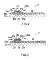
- FIGS 1,2 and 3 show a display electrode substrate 21 of the invention used for an active matrix display apparatus, in which a plurality of picture element electrodes 22 made of, for example, transparent ITO (indium tin oxide) or SnO2 are disposed in a matrix form. Each picture element electrode 22 is provided with first and second TFTs 20a and 20b, which are disposed in series as discussed below. As shown in Figures 2 and 3, on a glass substrate 25 is patterned a gate bus line 26 made of a metal material, such as tantalum, aluminum, molybdenum, titanium, chromium or tungsten.
- a metal material such as tantalum, aluminum, molybdenum, titanium, chromium or tungsten.
- the gate bus line 26 functions as a scanning line, on which a gate insulating film 27a made of, for example, tantalum oxide (Ta2O5) is disposed.
- a gate insulating film 27a made of, for example, tantalum oxide (Ta2O5) is disposed.
- a gate insulating layer 27b made of, for example, silicon nitride (SiNx), and are patterned semiconductor layers 28a and 28b made of intrinsic amorphous silicon (a-Si) or the like and etching stoppers 29a and 29b made of silicon nitride or the like in that order, the semiconductor layers 28a and 28b functioning as channel layers, respectively.
- semiconductor layers 28a and 28b and etching stoppers 29a and 29b are formed semiconductor layers 30a and 30b and 31a and 31b made of n-type amorphous silicon or the like for obtaining a good ohmic contact.
- semiconductor layers 30a, 30b, 31a, and 31b are formed source electrodes 33a and 33b and drain electrodes 34a and 34b, respectively.
- a source bus line 35 that is used as a signal line is patterned simultaneously with the source electrode 33a.
- two TFTs 20a and 20b corresponding to one picture element electrode 22 are disposed on the gate bus line 26.
- the source electrode 33a and drain electrode 34a at the first TFT 20a are positioned perpendicularly to the lengthwise direction of the gate bus line 26 and extend reversely to each other with respect to the gate bus line 26, and thus the channel direction of the first TFT 20a is perpendicular to the direction of the gate bus line 26.
- the source electrode 33a is one with the source bus line 35 and a wiring 43; namely the source electrode 33a is connected to the source bus line by means of the wiring 43 extending from the source bus line 35 in a direction that is parallel to the gate bus line 26.
- the source electrode 33b and drain electrode 34b of the second TFT 20b are positioned perpendicularly to the lengthwise direction of the gate bus line 26 and extend reversely to each other with respect to the gate bus line 26. Accordingly, the channel direction of the second TFT 20b is perpendicular to the direction of the gate bus line 26.
- the source electrode 33b is unitary with the drain electrode 34a and wiring 44; namely, the source electrode 33b is connected to the drain electrode 34a of the first TFT 20a by means of wiring 44 disposed in a direction parallel to the gate bus line 26.
- the drain electrodes 34b of the second TFT 20b is connected to the picture element electrode 22 disposed below the TFTs 20a and 20b in Figure 1.
- the electrical characteristics of the respective TFTs 20a and 20b depend upon configurations of channel regions formed between the source electrodes 33a and the drain electrode 34a and between those 33b and 34b.
- the electrical characteristics of the TFTs 20a and 20b significantly depend upon the ratios of W1a/L1a and W1b/L1b.
- a gate voltage applied to the gate bus line 26 switches on and off between the source electrode 33a and the drain electrode 34a and between the source electrode 33b and the drain electrode 34b.
- the gate bus line 26 is switched from a non-selection state to a selection state, current fed from the source bus line 35 flows to the picture element electrode 22 passing through the TFTs 20a and 20b.
- An opposite electrode is provided opposite to the picture element electrode 22 to sandwich a liquid crystal layer (not shown) therebetween, resulting in a capacitor.
- the capacitor is charged by the electric charge from the source bus line 35 and voltage by the charge is applied to the liquid crystal layer positioned between the opposite electrode and the picture element electrode 22, thereby changing optical characteristics of the liquid crystal layer.
- the light transmittance of the corresponding picture element at the active matrix display apparatus changes due to the change in the optical characteristics, thereby performing a desired display.
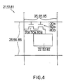
- Figure 4 shows the equivalent circuit of a portion corresponding to one picture element of the display electrode substrate 21.
- the other since two TFTs 20a and 20b are connected in series, even when one of the TFTs has a short-circuit defect, the other performs a normal switching operation, so that an electric charge, as normally supplied to the picture element electrode 22 corresponding to the TFTs, is still stored in the capacitor. Accordingly, the picture element corresponding to such a picture element electrode 22 does not become defective.
- the two TFTs 20a and 20b are juxtaposed on the same gate bus line 26 in the present embodiment, the area of the picture element electrode 22 is never reduced. In this way, the active matrix liquid crystal display apparatus using the display electrode substrate 21 can remarkably improve its display quality and production yield thereof.
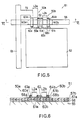
- FIGS 5 and 6 show another display electrode substrate 51 of the invention used for the active matrix display apparatus.
- the display electrode substrate 51 is manufactured in the same process as that of the aforesaid display electrode substrate 21 except for the patterning.
- a gate bus line 56 On a glass substrate 55 are provided a gate bus line 56, gate insulating films 57a and 57b, semiconductor layers 58a, 60a, 61a, 58b, 60b and 61b, and the like.
- first and second TFTs 50a and 50b corresponding to one picture element electrode 52 are connected in series on a gate bus line 56.
- a source electrode 63a of the first TFT 50a is unitary with a source busline 65 and a wiring 73; namely, the source electrode 63a is connected to the source bus line 65 by means of the wiring 73 extending from the source bus line 65 in a direction parallel to the gate bus line 56.
- a drain electrode 64b of the second TFT 50b is connected to the picture element electrode 52 disposed below the TFTs 50a and 50b in Figure 5.
- An electrode 62 that is disposed on a portion of the gate bus line 56 serves as the drain electrode 61a at the first TFT 50a and the source electrode 60b at the second TFT 50b.
- the equivalent circuit of the display electrode substrate 51 is shown in Figure 4, the display electrode 51 operating in the same way as that of the aforementioned display electrode substrate 21.
- the channel direction of the respective TFTs 50a and 50b is parallel to the gate bus line 56.
- the channel widths W2a and W2b of the TFTs 50a and 50b depend upon the width of the gate bus line 56, but the channel lengths L2a and L2b of the same can freely be set without increasing the area required for electric wiring, so that the TFTs 50a and 50b having desired electrical characteristics can be formed without reducing the area of picture element electrode 52. Therefore, the picture element defect caused by short-circuit of TFTs 50a and 50b is prevented and the effective area of the picture element electrode 52 is increasable, thereby improving the display quality of the display apparatus. Moreover, the display apparatus using the display electrode substrate 51 can expect high precision of image.
- Figures 7 and 8 show still another display electrode substrate 81 of the invention used for the active matrix liquid crystal display apparatus.
- the display electrode substrate 81 is manufactured by the same process as the aforesaid display electrode substrate 21 except for the patterning.
- a glass substrate 85 On a glass substrate 85 are provided a gate bus line 86, gate insulating films 87a and 87b, semiconductor layers 88a, 90a, 91a, 88b, 90b and 91b, and the like.
- first and second TFTs 80a and 80b corresponding to one picture element electrode 82 are disposed in series on a gate bus line 86.
- a source electrode 93a of the first TFT 80a is unitary with a source busline 95 and a wiring 103; namely, the source electrode 93a is connected to the source bus line 95 by means of the wiring 103 extending from the source bus line 95 in a direction that is parallel to the gate bus line 86.
- a source electrode 93b of the second TFT 80b is unitary with a drain electrode 94a of the first TFT 80a and a wiring 104; namely, the source electrode 93b is connected to the drain electrode 94a of the first TFT 80a by means of the wiring 104 disposed parallel to the gate bus line 86.
- a drain electrode 94b of the second TFT 80b is connected to a picture element 82 disposed below the TFTs 80a and 80b in Figure 7.
- the channel directions of the first and second TFTs 80a and 80b are parallel to the direction of the gate bus line 86.
- the equivalent circuit of the display electrode substrate 81 is shown in Figure 4, the substrate 81 operating in the same way as that of the aforesaid display electrode substrates 21 and 51.
- the effective area of the picture element electrode 82 is increasable and its display quality is improvable.
- the wiring 104 connected to the drain electrode 94a is connected to the source electrode 93b in a manner to extend round the drain electrode 94b at the TFT 80b, so that the semiconductor layers 88a and 88b are completely separated from each other, thereby enabling the TFTs 80a and 80b to reliably operate and attaining an improvement of reliability thereof.
- the display electrode substrate is provided with a lengthy construction in which two TFTs are connected in series, whereby the picture element defect caused by a short-circuit at the TFTs is prevented and the production yield of the display electrode substrate is improved.
- a plurality of TFTs are connected in series to each picture element electrode, so that the electric charge is supplied to the picture element electrode and stored in the capacitor even when some of the TFTs cause a short-circuit defect. Accordingly, the picture element defect caused by a short-circuit at the TFTs can be remarkably reduced.
Landscapes
- Physics & Mathematics (AREA)
- Engineering & Computer Science (AREA)
- Nonlinear Science (AREA)
- Microelectronics & Electronic Packaging (AREA)
- Power Engineering (AREA)
- General Physics & Mathematics (AREA)
- Mathematical Physics (AREA)
- Crystallography & Structural Chemistry (AREA)
- Optics & Photonics (AREA)
- Condensed Matter Physics & Semiconductors (AREA)
- Chemical & Material Sciences (AREA)
- Computer Hardware Design (AREA)
- Liquid Crystal (AREA)
- Thin Film Transistor (AREA)
- Devices For Indicating Variable Information By Combining Individual Elements (AREA)
Abstract
Description
- The present invention relates to a display electrode substrate that is suitable for use in an active matrix display apparatus.
- Fig. 9 of the drawings is a plan view of a conventional display electrode substrate used for an active matrix liquid crystal display apparatus, showing a structure of the substrate per one picture element, and Figure 10 is a sectional view taken on the line X-X in Figure 9, wherein on a transparent
insulating substrate 1 is formed agate bus line 2 as a scanning line for the active matrix liquid crystal display apparatus, and part of thegate bus line 2 functions as a gate electrode of a thin film transistor (TFT) 8. A gateinsulating film 3a of tantalum oxide (Ta₂O₅) coats thegate bus line 2. Agate insulating film 3b is disposed throughout the surface ofsubstrate 1 including thegate insulating film 3a. - A
semiconductor layer 4 made of intrinsic amorphous silicon or the like is disposed at a position on thegate insulating film 3b that corresponds to thegate bus line 2.Semiconductor layers semiconductor layer 4. Also, thesemiconductor layer 4 is a channel layer ofTFT 8. On thegate insulating film 3b are integrally disposed asource bus line 5 and asource electrode 5a functioning as the signal lines at the active matrix liquid crystal display apparatus. Thesource bus line 5 is disposed to perpendicularly cross over thegate bus line 2 so as to sandwich thegate insulating film 3b therebetween. Thesource electrode 5a is superposed on a lateral side of thesemiconductor layer 4. Adrain electrode 6 is disposed on thegate insulating film 3b in such a manner that part of thedrain electrode 6 is disposed on the other side of thesemiconductor layer 4. - Moreover, on the
gate insulating film 3b is disposed apicture element electrode 7 made of a transparent conductive film and having an area corresponding to one picture element, thepicture element electrode 7 being disposed on part of thedrain electrode 6 to be electrically connected therewith. - The
gate bus line 2, gateinsulating films semiconductor layers source electrode 5a anddrain electrode 6 constitute theTFT 8. TheTFT 8 functions as a switch element corresponding to one picture element at the active matrix liquid crystal display apparatus. The electrical characteristics ofTFT 8 depend upon the width W1 ofsource electrode 5a anddrain electrode 6 and the distance (channel length) L1 between thesource electrode 5a and thedrain eleectrode 6. - The
TFT 8 and thepicture element electrode 7 are disposed at every intersection of thegate bus line 2 andsource bus line 5, in other words, as many as the number of picture elements disposed in a matrix form. A liquid crystal layer is sandwiched between the display electrode substrate thus formed and an opposite substrate on which the opposite electrode is disposed, thereby constituting a transparent type active matrix liquid crystal display apparatus. - The number of
TFTs 8 formed on the aforesaid display electrode substrate depends upon the number of picture elements. For example, for the liquid crystal display apparatus of 400 x 64 dots, 256000TFTs 8 must be disposed in a matrix form. With the display electrode substrate having suchnumerous TFTs 8, if even oneTFT 8 among them causes a malfunction, the picture element corresponding to thedefective TFT 8 becomes defective, so that the display quality of the liquid crystal display apparatus is lowered. Accordingly, all of thenumerous TFTs 8 must be formed without any defect. - However, the process for producing the display electrode substrate is complicated as mentioned above, so that it is difficult to form
numerous TFTs 8 on the insulating substrate of a large area without defects, which lowers the production yield of the display electrode substrates. - As an approach for improving the production yield of the display electrode substrate, it has been proposed to provide two or
more TFTs 8 per picture element so as to produce a redundant structure. - Figure 11 is a plan view of the display electrode substrate of a redundant structure, showing a construction per a picture element, in which the components corresponding to those in Figure 10 are designated with the same reference numerals.
- The display electrode substrate is provided with a
TFT 18 in addition to theTFT 8, corresponding to eachpicture element electrode 7, theTFT 18 being patterned simultaneously with theTFT 8 in the aforesaid manufacturing process for the display electrode substrate. Accordingly, the TFT 18 is constituted by thebus line 2,semiconductor layers source electrode 5b anddrain electrode 16. - The
source electrode 5b at theTFT 18 is integrally disposed with thesource bus line 5 andsource electrode 5a, a portion of thesource electrode 5b being disposed on one side of the semiconductor layer 14. A picture element electrode is disposed on one end of thedrain electrode 16, the other end of thedrain electrode 16 overlapping the other side of the semiconductor layer 14. - In the display electrode substrate, even when, for example, one of a plurality of
TFTs - When two or
more TFTs - The display electrode substrate of this invention comprises a large number of picture element electrodes disposed in a matrix form on an insulating substrate, at least two, first and second, thin film transistors connected to each of said picture element electrodes, gate bus lines provided in parallel to each other between said picture element electrodes, and source bus lines intersecting with said gate bus lines respectively, wherein said first and second thin film transistors are juxtaposed on the same one of said gate bus lines, part of said gate bus line functions as gate electrodes of said first and second thin film transistors, a source electrode of said first thin film transistor is connected to said source bus line, a drain electrode of said first thin film transistor is connected to a source electrode of said second thin film transistor, and a drain electrode of said second thin film transistor is connected to said picture element electrode.
- In a preferred embodiment, the source electrodes and drain electrodes at said first and second thin film transistors are positioned reversely to each other with respect to said gate bus wiring, the channel directions of said first and second thin film transistors being perpendicular to the extending direction of said gate bus line.
- In a preferred embodiment, the source electrode and drain electrode at each of first and second thin film transistors are positioned in the extending direction of said gate bus wiring, the channel directions of said first and second thin film transistors being parallel to the extending direction of said gate bus line. The drain electrode at said first thin film transistor and said source electrode at said second thin film transistor are positioned adjacently to each other on said gate bus line. Alternatively, the drain electride at said first thin film transistor and said drain electrode at said second thin film transistor are positioned adjacently to each other on said gate bus line.
- According to the present invention, since a plurality of TFTs are connected in series to each picture element, even when some of these TFTs cause a short-circuit defect, the remaining TFTs that are normally operable can supply the electric charge to the corresponding picture element electrode and the electrode charge is stored in the capacitor.
- Thus, the invention described herein makes possible the objective of providing a display electrode substrate that can reduce a picture element defect caused by a short-circuit defect of the TFTs.
- This invention will be further described, by way of example, with reference to the accompanying drawings, of which Figs. 9 to 11 have already been described and in which:-
- Figure 1 is a plan view showing a portion of a display electrode substrate of the present invention;
- Figure 2 is a sectional view taken along the line II-II of Figure 1;
- Figure 3 is a sectional view taken along the line III-III of Figure 1;
- Figure 4 is an equivalent circuit of a portion corresponding to one picture element of the display electrode substrate of the present invention;
- Figure 5 is a plan view showing a portion of another display electrode substrate of the present invention;
- Figure 6 is a sectional view taken along the line VI-VI of Figure 5;
- Figure 7 is a plan view showing a portion of still another display electrode substrate of the present invention;
- Figure 8 is a sectional view taken along the line VIII-VIII of Figure 7;
- Figure 9 is a plan view showing a portion of a conventional display electrode substrate that does not have a redundant structure;
- Figure 10 is a sectional view taken along the line X-X of Figure 9; and
- Figure 11 is a plan view showing a portion of another display electrode substrate with a redundant structure.
- Figures 1,2 and 3 show a
display electrode substrate 21 of the invention used for an active matrix display apparatus, in which a plurality ofpicture element electrodes 22 made of, for example, transparent ITO (indium tin oxide) or SnO₂ are disposed in a matrix form. Eachpicture element electrode 22 is provided with first andsecond TFTs glass substrate 25 is patterned agate bus line 26 made of a metal material, such as tantalum, aluminum, molybdenum, titanium, chromium or tungsten. Thegate bus line 26 functions as a scanning line, on which agate insulating film 27a made of, for example, tantalum oxide (Ta₂O₅) is disposed. On the entire surface of thegate insulating film 27a is disposed agate insulating layer 27b made of, for example, silicon nitride (SiNx), and are patternedsemiconductor layers etching stoppers semiconductor layers - On the
semiconductor layers etching stoppers semiconductor layers semiconductor layers source electrodes drain electrodes source bus line 35 that is used as a signal line is patterned simultaneously with thesource electrode 33a. - As shown in Figure 1, in the
display electrode substrate 21, twoTFTs picture element electrode 22 are disposed on thegate bus line 26. Thesource electrode 33a anddrain electrode 34a at thefirst TFT 20a are positioned perpendicularly to the lengthwise direction of thegate bus line 26 and extend reversely to each other with respect to thegate bus line 26, and thus the channel direction of thefirst TFT 20a is perpendicular to the direction of thegate bus line 26. Thesource electrode 33a is one with thesource bus line 35 and awiring 43; namely thesource electrode 33a is connected to the source bus line by means of thewiring 43 extending from thesource bus line 35 in a direction that is parallel to thegate bus line 26. - The
source electrode 33b anddrain electrode 34b of thesecond TFT 20b are positioned perpendicularly to the lengthwise direction of thegate bus line 26 and extend reversely to each other with respect to thegate bus line 26. Accordingly, the channel direction of thesecond TFT 20b is perpendicular to the direction of thegate bus line 26. Thesource electrode 33b is unitary with thedrain electrode 34a and wiring 44; namely, thesource electrode 33b is connected to thedrain electrode 34a of thefirst TFT 20a by means of wiring 44 disposed in a direction parallel to thegate bus line 26. Thedrain electrodes 34b of thesecond TFT 20b is connected to thepicture element electrode 22 disposed below theTFTs - With the above-mentioned
display electrode substrate 21, the electrical characteristics of therespective TFTs source electrodes 33a and thedrain electrode 34a and between those 33b and 34b. In other words, as shown in Figure 1, when the breadth of thesource electrode 33a and drainelectrode 34a and the breadth of thesource electrode 33b anddrain electrode 34b are represented by channel widths W1a and W1b, respectively, and the distance between thesource electrode 33a and thedrain electrode 34a and the distance between thesource electrode 33b and thedrain electrode 34b are represented by channel lengths L1a and L1b, respectively, the electrical characteristics of theTFTs TFTs TFTs TFT 8 at the display electrode substrate described with reference to Figure 9, the channel widths W1a and W1b and channel lengths L1a and L1b are set to satisfy the relation given in the following equation:
L1a/W1a + L1b/W1b = L1/W1 (1)
The channel lengths L1a and L1b depend upon the width of thegate bus line 26, and thus, when L1 = L1a = L1b and moreover W1a = W1b are set, the channel widths W1a and W1b are given in the following formula:
W1a = W1b = 2 · W1 (2) - In the active matrix type display apparatus using the above-mentioned
display electrode substrate 21, a gate voltage applied to thegate bus line 26 switches on and off between thesource electrode 33a and thedrain electrode 34a and between thesource electrode 33b and thedrain electrode 34b. For example, when thegate bus line 26 is switched from a non-selection state to a selection state, current fed from thesource bus line 35 flows to thepicture element electrode 22 passing through theTFTs picture element electrode 22 to sandwich a liquid crystal layer (not shown) therebetween, resulting in a capacitor. Accordingly, the capacitor is charged by the electric charge from thesource bus line 35 and voltage by the charge is applied to the liquid crystal layer positioned between the opposite electrode and thepicture element electrode 22, thereby changing optical characteristics of the liquid crystal layer. Hence, the light transmittance of the corresponding picture element at the active matrix display apparatus changes due to the change in the optical characteristics, thereby performing a desired display. - Figure 4 shows the equivalent circuit of a portion corresponding to one picture element of the
display electrode substrate 21. As shown in Figure 4, since twoTFTs picture element electrode 22 corresponding to the TFTs, is still stored in the capacitor. Accordingly, the picture element corresponding to such apicture element electrode 22 does not become defective. Moreover, as shown in Figure 1, the twoTFTs gate bus line 26 in the present embodiment, the area of thepicture element electrode 22 is never reduced. In this way, the active matrix liquid crystal display apparatus using thedisplay electrode substrate 21 can remarkably improve its display quality and production yield thereof. - Figures 5 and 6 show another
display electrode substrate 51 of the invention used for the active matrix display apparatus. - The
display electrode substrate 51 is manufactured in the same process as that of the aforesaiddisplay electrode substrate 21 except for the patterning. On aglass substrate 55 are provided agate bus line 56,gate insulating films semiconductor layers - At the
display electrode substrate 51, first andsecond TFTs picture element electrode 52 are connected in series on agate bus line 56. Asource electrode 63a of thefirst TFT 50a is unitary with asource busline 65 and awiring 73; namely, thesource electrode 63a is connected to thesource bus line 65 by means of thewiring 73 extending from thesource bus line 65 in a direction parallel to thegate bus line 56. Adrain electrode 64b of thesecond TFT 50b is connected to thepicture element electrode 52 disposed below theTFTs - An
electrode 62 that is disposed on a portion of thegate bus line 56 serves as thedrain electrode 61a at thefirst TFT 50a and thesource electrode 60b at thesecond TFT 50b. The equivalent circuit of thedisplay electrode substrate 51 is shown in Figure 4, thedisplay electrode 51 operating in the same way as that of the aforementioneddisplay electrode substrate 21. - The channel direction of the
respective TFTs gate bus line 56. The channel widths W2a and W2b of theTFTs gate bus line 56, but the channel lengths L2a and L2b of the same can freely be set without increasing the area required for electric wiring, so that theTFTs picture element electrode 52. Therefore, the picture element defect caused by short-circuit ofTFTs picture element electrode 52 is increasable, thereby improving the display quality of the display apparatus. Moreover, the display apparatus using thedisplay electrode substrate 51 can expect high precision of image. - Figures 7 and 8 show still another
display electrode substrate 81 of the invention used for the active matrix liquid crystal display apparatus. - The
display electrode substrate 81 is manufactured by the same process as the aforesaiddisplay electrode substrate 21 except for the patterning. On aglass substrate 85 are provided agate bus line 86,gate insulating films semiconductor layers - At the
display electrode substrate 81, first andsecond TFTs picture element electrode 82 are disposed in series on agate bus line 86. Asource electrode 93a of thefirst TFT 80a is unitary with asource busline 95 and awiring 103; namely, thesource electrode 93a is connected to thesource bus line 95 by means of thewiring 103 extending from thesource bus line 95 in a direction that is parallel to thegate bus line 86. - A
source electrode 93b of thesecond TFT 80b is unitary with adrain electrode 94a of thefirst TFT 80a and awiring 104; namely, thesource electrode 93b is connected to thedrain electrode 94a of thefirst TFT 80a by means of thewiring 104 disposed parallel to thegate bus line 86. Adrain electrode 94b of thesecond TFT 80b is connected to apicture element 82 disposed below theTFTs second TFTs gate bus line 86. The equivalent circuit of thedisplay electrode substrate 81 is shown in Figure 4, thesubstrate 81 operating in the same way as that of the aforesaiddisplay electrode substrates - At the
display electrode substrate 81, since theTFTs 80a and 81b are juxtaposed on thegate bus line 86, the area required for wiring is not increased for the same reasons as those of the aforesaiddisplay electrode substrate 51. Accordingly, the effective area of thepicture element electrode 82 is increasable and its display quality is improvable. Moreover, with the twoTFTs display electrode substrate 81, thewiring 104 connected to thedrain electrode 94a is connected to thesource electrode 93b in a manner to extend round thedrain electrode 94b at theTFT 80b, so that the semiconductor layers 88a and 88b are completely separated from each other, thereby enabling theTFTs - As mentioned above, the display electrode substrate is provided with a lengthy construction in which two TFTs are connected in series, whereby the picture element defect caused by a short-circuit at the TFTs is prevented and the production yield of the display electrode substrate is improved.
- Although these embodiments disclose that two TFTs are disposed on the gate bus line which is used as the gate electrode, the number of TFTs connected in series is not be limited thereto. Moreover, it is posible that a plurality of TFTs connected in series are connected in parallel.
- As seen from the above, according to the present invention, a plurality of TFTs are connected in series to each picture element electrode, so that the electric charge is supplied to the picture element electrode and stored in the capacitor even when some of the TFTs cause a short-circuit defect. Accordingly, the picture element defect caused by a short-circuit at the TFTs can be remarkably reduced.
- It is understood that various other modifications will be apparent to and can be readily made by those skilled in the art without departing from the scope and spirit of this invention. Accordingly, it is not intended that the scope of the claims appended hereto be limited to the description as set forth herein, but rather that the claims be construed as encompassing all the features of patentable novelty that reside in the present invention, including all features that would be treated as equivalents thereof by those skilled in the art to which this invention pertains.
Claims (5)
Applications Claiming Priority (2)
| Application Number | Priority Date | Filing Date | Title |
|---|---|---|---|
| JP1064289A JP2834756B2 (en) | 1989-01-18 | 1989-01-18 | Display electrode substrate |
| JP10642/89 | 1989-01-18 |
Publications (2)
| Publication Number | Publication Date |
|---|---|
| EP0379366A1 true EP0379366A1 (en) | 1990-07-25 |
| EP0379366B1 EP0379366B1 (en) | 1994-09-14 |
Family
ID=11755866
Family Applications (1)
| Application Number | Title | Priority Date | Filing Date |
|---|---|---|---|
| EP90300520A Expired - Lifetime EP0379366B1 (en) | 1989-01-18 | 1990-01-18 | A display electrode substrate |
Country Status (4)
| Country | Link |
|---|---|
| US (1) | US5410164A (en) |
| EP (1) | EP0379366B1 (en) |
| JP (1) | JP2834756B2 (en) |
| DE (1) | DE69012356T2 (en) |
Cited By (2)
| Publication number | Priority date | Publication date | Assignee | Title |
|---|---|---|---|---|
| EP0721214A2 (en) * | 1995-01-03 | 1996-07-10 | Xerox Corporation | Circuitry with gate line crossing semiconductor line at two or more channels |
| US6566684B1 (en) | 1994-06-13 | 2003-05-20 | Semiconductor Energy Laboratory Co., Ltd. | Active matrix circuit having a TFT with pixel electrode as auxiliary capacitor |
Families Citing this family (11)
| Publication number | Priority date | Publication date | Assignee | Title |
|---|---|---|---|---|
| JP2794678B2 (en) | 1991-08-26 | 1998-09-10 | 株式会社 半導体エネルギー研究所 | Insulated gate semiconductor device and method of manufacturing the same |
| CN1230919C (en) * | 1994-06-02 | 2005-12-07 | 株式会社半导体能源研究所 | Active matrix display device and electrooptical element |
| US5929464A (en) * | 1995-01-20 | 1999-07-27 | Semiconductor Energy Laboratory Co., Ltd. | Active matrix electro-optical device |
| JPH09298305A (en) * | 1996-05-08 | 1997-11-18 | Semiconductor Energy Lab Co Ltd | Thin film transistor and liq. crystal display having such thin film transistor |
| US5808317A (en) * | 1996-07-24 | 1998-09-15 | International Business Machines Corporation | Split-gate, horizontally redundant, and self-aligned thin film transistors |
| JP5004606B2 (en) * | 2006-05-31 | 2012-08-22 | 株式会社ジャパンディスプレイイースト | Display device |
| US8279151B2 (en) | 2006-05-31 | 2012-10-02 | Hitachi Displays, Ltd. | Display device |
| JP2008060312A (en) * | 2006-08-31 | 2008-03-13 | Sanyo Electric Co Ltd | Field effect transistor and manufacturing method therefor |
| US7842920B2 (en) * | 2006-12-14 | 2010-11-30 | Dcg Systems, Inc. | Methods and systems of performing device failure analysis, electrical characterization and physical characterization |
| CN103811503A (en) | 2014-02-19 | 2014-05-21 | 合肥鑫晟光电科技有限公司 | Array substrate and preparation method and display panel |
| US11209707B2 (en) * | 2019-10-22 | 2021-12-28 | Sharp Kabushiki Kaisha | Display device |
Citations (5)
| Publication number | Priority date | Publication date | Assignee | Title |
|---|---|---|---|---|
| EP0182645A1 (en) * | 1984-11-16 | 1986-05-28 | Matsushita Electric Industrial Co., Ltd. | Active matrix circuit for liquid crystal displays |
| EP0259875A2 (en) * | 1986-09-11 | 1988-03-16 | Fujitsu Limited | Active matrix display devices |
| US4762398A (en) * | 1987-01-26 | 1988-08-09 | Hosiden Electronics Co., Ltd. | Pixel transistor free of parasitic capacitance fluctuations from misalignment |
| US4775861A (en) * | 1984-11-02 | 1988-10-04 | Nec Corporation | Driving circuit of a liquid crystal display panel which equivalently reduces picture defects |
| GB2206721A (en) * | 1987-07-03 | 1989-01-11 | Philips Electronic Associated | Active matrix display device |
Family Cites Families (10)
| Publication number | Priority date | Publication date | Assignee | Title |
|---|---|---|---|---|
| JPS61174508A (en) * | 1985-01-30 | 1986-08-06 | Seiko Epson Corp | Liquid-crystal display element |
| JPH0740101B2 (en) * | 1985-04-23 | 1995-05-01 | 旭硝子株式会社 | Thin film transistor |
| JPH06103372B2 (en) * | 1985-05-16 | 1994-12-14 | 旭硝子株式会社 | Thin film active device substrate |
| JPS62135814A (en) * | 1985-12-10 | 1987-06-18 | Fuji Electric Co Ltd | Liquid crystal matrix display device |
| JP2563774B2 (en) * | 1985-12-19 | 1996-12-18 | セイコーエプソン株式会社 | Projection display device |
| JPS63151083A (en) * | 1986-12-16 | 1988-06-23 | Hitachi Ltd | Thin film semiconductor device |
| JPS63263743A (en) * | 1987-04-22 | 1988-10-31 | Alps Electric Co Ltd | Thin film transistor array and manufacture thereof |
| JPS6450028A (en) * | 1987-08-21 | 1989-02-27 | Nec Corp | Thin film transistor substrate |
| JPH01161316A (en) * | 1987-12-18 | 1989-06-26 | Sharp Corp | Liquid crystal display device |
| US4917467A (en) * | 1988-06-16 | 1990-04-17 | Industrial Technology Research Institute | Active matrix addressing arrangement for liquid crystal display |
-
1989
- 1989-01-18 JP JP1064289A patent/JP2834756B2/en not_active Expired - Lifetime
-
1990
- 1990-01-18 DE DE69012356T patent/DE69012356T2/en not_active Expired - Fee Related
- 1990-01-18 EP EP90300520A patent/EP0379366B1/en not_active Expired - Lifetime
-
1992
- 1992-01-02 US US07/816,856 patent/US5410164A/en not_active Expired - Lifetime
Patent Citations (5)
| Publication number | Priority date | Publication date | Assignee | Title |
|---|---|---|---|---|
| US4775861A (en) * | 1984-11-02 | 1988-10-04 | Nec Corporation | Driving circuit of a liquid crystal display panel which equivalently reduces picture defects |
| EP0182645A1 (en) * | 1984-11-16 | 1986-05-28 | Matsushita Electric Industrial Co., Ltd. | Active matrix circuit for liquid crystal displays |
| EP0259875A2 (en) * | 1986-09-11 | 1988-03-16 | Fujitsu Limited | Active matrix display devices |
| US4762398A (en) * | 1987-01-26 | 1988-08-09 | Hosiden Electronics Co., Ltd. | Pixel transistor free of parasitic capacitance fluctuations from misalignment |
| GB2206721A (en) * | 1987-07-03 | 1989-01-11 | Philips Electronic Associated | Active matrix display device |
Cited By (3)
| Publication number | Priority date | Publication date | Assignee | Title |
|---|---|---|---|---|
| US6566684B1 (en) | 1994-06-13 | 2003-05-20 | Semiconductor Energy Laboratory Co., Ltd. | Active matrix circuit having a TFT with pixel electrode as auxiliary capacitor |
| EP0721214A2 (en) * | 1995-01-03 | 1996-07-10 | Xerox Corporation | Circuitry with gate line crossing semiconductor line at two or more channels |
| EP0721214A3 (en) * | 1995-01-03 | 1998-06-03 | Xerox Corporation | Circuitry with gate line crossing semiconductor line at two or more channels |
Also Published As
| Publication number | Publication date |
|---|---|
| US5410164A (en) | 1995-04-25 |
| JP2834756B2 (en) | 1998-12-14 |
| DE69012356D1 (en) | 1994-10-20 |
| JPH02189522A (en) | 1990-07-25 |
| EP0379366B1 (en) | 1994-09-14 |
| DE69012356T2 (en) | 1995-03-16 |
Similar Documents
| Publication | Publication Date | Title |
|---|---|---|
| KR960014498B1 (en) | Active matrix lcd cell giving bright image and panel having active matrix lcd cell | |
| US5162901A (en) | Active-matrix display device with added capacitance electrode wire and secondary wire connected thereto | |
| EP0376437B1 (en) | An active matrix type liquid crystal display | |
| KR100260359B1 (en) | Lcd and method for manufacturing the same | |
| US5751381A (en) | Active matrix LCD device with image signal lines having a multilayered structure | |
| KR100266189B1 (en) | Amlcd panel and wiring designing method therefor | |
| KR100241487B1 (en) | Active matrix type liquid crystal display device and method of correcting for defective pixel | |
| US5231039A (en) | Method of fabricating a liquid crystal display device | |
| EP0329887B1 (en) | Liquid crystal display device | |
| EP0166948B1 (en) | Displays and subassemblies having improved pixel electrodes | |
| KR940010414B1 (en) | Liquid crystal display device having metallic bus repair layer | |
| US5047819A (en) | Amorphous-silicon thin film transistor array substrate | |
| EP0514218B1 (en) | An active matrix substrate | |
| EP0379366B1 (en) | A display electrode substrate | |
| JP2003307748A (en) | Liquid crystal display device and manufacturing method thereof | |
| EP0315319B1 (en) | Liquid crystal display device | |
| JP4703258B2 (en) | Thin film transistor substrate and liquid crystal display panel | |
| KR940008248B1 (en) | Liquid crystal display device | |
| US5286983A (en) | Thin-film-transistor array with capacitance conductors | |
| US5508765A (en) | Matrix-addressed type display device | |
| JPH02277027A (en) | Liquid crystal display device | |
| EP0430418A2 (en) | Liquid crystal display and method of manufacturing the same | |
| JP2002090775A (en) | Matrix array substrate | |
| JPH06163891A (en) | Thin film transistor | |
| KR100229610B1 (en) | Lcd device and its manufacturing method |
Legal Events
| Date | Code | Title | Description |
|---|---|---|---|
| PUAI | Public reference made under article 153(3) epc to a published international application that has entered the european phase |
Free format text: ORIGINAL CODE: 0009012 |
|
| 17P | Request for examination filed |
Effective date: 19900203 |
|
| AK | Designated contracting states |
Kind code of ref document: A1 Designated state(s): DE FR GB NL |
|
| 17Q | First examination report despatched |
Effective date: 19921221 |
|
| GRAA | (expected) grant |
Free format text: ORIGINAL CODE: 0009210 |
|
| AK | Designated contracting states |
Kind code of ref document: B1 Designated state(s): DE FR GB NL |
|
| REF | Corresponds to: |
Ref document number: 69012356 Country of ref document: DE Date of ref document: 19941020 |
|
| ET | Fr: translation filed | ||
| PLBE | No opposition filed within time limit |
Free format text: ORIGINAL CODE: 0009261 |
|
| STAA | Information on the status of an ep patent application or granted ep patent |
Free format text: STATUS: NO OPPOSITION FILED WITHIN TIME LIMIT |
|
| 26N | No opposition filed | ||
| REG | Reference to a national code |
Ref country code: GB Ref legal event code: IF02 |
|
| PGFP | Annual fee paid to national office [announced via postgrant information from national office to epo] |
Ref country code: FR Payment date: 20020110 Year of fee payment: 13 |
|
| PGFP | Annual fee paid to national office [announced via postgrant information from national office to epo] |
Ref country code: GB Payment date: 20020116 Year of fee payment: 13 |
|
| PGFP | Annual fee paid to national office [announced via postgrant information from national office to epo] |
Ref country code: NL Payment date: 20020131 Year of fee payment: 13 |
|
| PGFP | Annual fee paid to national office [announced via postgrant information from national office to epo] |
Ref country code: DE Payment date: 20020227 Year of fee payment: 13 |
|
| PG25 | Lapsed in a contracting state [announced via postgrant information from national office to epo] |
Ref country code: GB Free format text: LAPSE BECAUSE OF NON-PAYMENT OF DUE FEES Effective date: 20030118 |
|
| PG25 | Lapsed in a contracting state [announced via postgrant information from national office to epo] |
Ref country code: NL Free format text: LAPSE BECAUSE OF NON-PAYMENT OF DUE FEES Effective date: 20030801 Ref country code: DE Free format text: LAPSE BECAUSE OF NON-PAYMENT OF DUE FEES Effective date: 20030801 |
|
| GBPC | Gb: european patent ceased through non-payment of renewal fee | ||
| PG25 | Lapsed in a contracting state [announced via postgrant information from national office to epo] |
Ref country code: FR Free format text: LAPSE BECAUSE OF NON-PAYMENT OF DUE FEES Effective date: 20030930 |
|
| NLV4 | Nl: lapsed or anulled due to non-payment of the annual fee |
Effective date: 20030801 |
|
| REG | Reference to a national code |
Ref country code: FR Ref legal event code: ST |