EP0377976B1 - Dispositif de commande microprogrammé utilisant des circuits à réseaux logiques programmables - Google Patents
Dispositif de commande microprogrammé utilisant des circuits à réseaux logiques programmables Download PDFInfo
- Publication number
- EP0377976B1 EP0377976B1 EP89313061A EP89313061A EP0377976B1 EP 0377976 B1 EP0377976 B1 EP 0377976B1 EP 89313061 A EP89313061 A EP 89313061A EP 89313061 A EP89313061 A EP 89313061A EP 0377976 B1 EP0377976 B1 EP 0377976B1
- Authority
- EP
- European Patent Office
- Prior art keywords
- pla
- output
- partition
- states
- data bits
- Prior art date
- Legal status (The legal status is an assumption and is not a legal conclusion. Google has not performed a legal analysis and makes no representation as to the accuracy of the status listed.)
- Expired - Lifetime
Links
Images


Classifications
-
- G—PHYSICS
- G06—COMPUTING; CALCULATING OR COUNTING
- G06F—ELECTRIC DIGITAL DATA PROCESSING
- G06F9/00—Arrangements for program control, e.g. control units
- G06F9/06—Arrangements for program control, e.g. control units using stored programs, i.e. using an internal store of processing equipment to receive or retain programs
- G06F9/22—Microcontrol or microprogram arrangements
- G06F9/223—Execution means for microinstructions irrespective of the microinstruction function, e.g. decoding of microinstructions and nanoinstructions; timing of microinstructions; programmable logic arrays; delays and fan-out problems
Definitions
- This invention relates to microcode control apparatus for use in microprogrammed data processors and digital computers wherein a sequence of microwords is used to control the execution of each of the processor instructions.
- microwords In a microprogrammed data processor, microwords, or microinstructions, are read from an internal storage unit to provide internal processor control actions for executing the processor instructions obtained from a user's software program.
- the microwords are read from the storage unit and written to a control register one at a time.
- Each microword consists of multiple binary bits, some or all of which may be organized into plural-bit control groups or fields.
- the control register provides control point signals which, in turn, control the various data flow rate and data manipulation mechanisms within the data processor, with each microword controlling the internal operation of the data processor for one microword cycle.
- Several microwords are usually needed to execute each processor instruction. Some processor instructions require only a few microwords, while others require many.
- microwords may be located in a separate so called portion of the processor's main memory set aside for the exclusive use of the microwords. Furthermore, microwords may also be stored in read only storage units (ROS).
- ROI read only storage units
- control storage unit and its associated addressing circuitry can be replaced by a programmable logic array (PLA), working in conjunction with a sequence counter.
- the PLA is driven by an operation code portion of the processor instruction and a particular sequence count from the sequence counter for producing a particular microword at its output.
- Such a PLA and sequence counter combination is able to provide significant savings in the size of the real estate (in terms of the area within the data processor) required -- when the PLA is compared to the conventional storage unit. If a desired number of repetitions for a certain microcode is needed, a fixed capacity repeat counter for counting the number of microcode loops in order to terminate the looping action at a certain count is also required. For different types of processor instructions where the number of microcode loops are different, a different number of fixed capacity repeat counters may also be needed, thereby further burdening the data processor.
- U.S. Patent 4,556,938 discloses the use of a programmable repeat counter which can be loaded with different initial count values for different processor instructions, in order to provide different numbers of repeats for the different microcode loops needed for the different instructions. Although such an arrangement is able to reduce the amount of circuitry needed in those situations where microcode looping is provided for two or more different processor instructions, the fact remains that -- when working in concert with the programmable repeat counter -- the PLA can only generate one microword at a time.
- US-A-3959774 discloses an arrangement for organising a computer in which program instructions are generated outside the cpu using a number of PLAs.
- a PLA including a master program can call other PLAs including subroutines and these PLAs including subroutines can call PLAs including other subroutine as in a conventional computer program.
- This invention provides a microcode control apparatus for a data processor wherein microwords are used to effect execution of processor instructions, the apparatus comprising: a first PLA having an input partition containing a plurality of states for receiving an operation code of a processor instruction, sequencing means for incrementing the states of the input partition, and an output partition for generating output sets of data bits corresponding to the number of states present in the input partition; at least a second PLA having an input partition containing a plurality of states for receiving a set of data bits from the output partition of the first PLA, sequencing means for incrementing the states of the input partition, and an output partition for generating output sets of data bits corresponding to the number of states present in the input partition; wherein at least a predefined portion of the output sets of data bits of the first PLA is provided as input to the input partition of the second PLA, the second PLA being arranged so that operation thereof is initiated when said predefined portion of the output sets of data bits of the first PLA corresponds to a predefined encode number, the output partition of the second PLA providing at least one control signal,
- PLA logic array
- the mainline PLA in controlling the subroutine PLAs, utilizes an encoded number, in the form of a multiple number of data bits, provided from its output partition (OR array) to the input partition (AND array) of the subroutine PLA(s) it is addressing.
- the addressed subroutine PLA becomes operative if the encoded number data bits from the mainline PLA match predetermined data bits in its encoded number field. At that point, the mainline PLA goes into a state of suspension (although control point signals are still being output therefrom), while the states ( i.e. the addresses) of the addressed subroutine PLA are incremented to perform the operation it is preprogrammed for.
- the subroutine PLA continues to implement the operation and provide as its output the necessary control points, until it has been incremented by its corresponding sequence counter into a state whereby it is informed that the operation no longer needs to be implemented (or that the operation is finished). At that time, a data bit is sent from the subroutine PLA to the mainline PLA for automatically reinitializing, or reinstating, the incrementation of the mainline PLA.
- subroutine PLAs which can perform different operations
- mainline PLA can be addressed by the mainline PLA.
- additional subroutine PLAs can be positioned, relative to the mainline PLA, at different levels.
- an unlimited number of subroutine PLAs can be nested together such that a plurality of different levels of subroutine PLAs can be commanded by the same mainline PLA for performing different operations, at the same or different times via different subroutines.
- Another object and advantage provided by the present invention is the automatic branching back to the point in the mainline PLA where the subroutine PLA was addressed, after the operation performed by the subroutine PLA has been completed, and without using any kind of address return "save" mechanism.
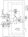
- FIG. 1 shows a broad overview of a prior art data processor.
- Data processor 2 includes a data flow unit 4, a main memory 6, an input/output unit 8 and a simplified control unit 10.
- Data flow unit 4 may sometimes be referred to as a central processing unit (CPU) and may include such things as an arithmetic logic unit (ALU), various hardware registers, storage units and a bus system interconnecting the different units for controlling the movement of data between the same. In essence, data flow unit 4 performs the actual manipulation of the data to produce the desired results.
- data flow unit 4 is connected to main memory 6 and I/O unit 8, respectively, for transporting information to and from these units.
- the software program, or user program, containing the instructions to be executed, is loaded into main memory 6.
- the processor instructions contained within the user program are read out of main memory 6 and supplied to data flow unit 4, one at a time and in a sequential manner, for performing the desired operations.
- data flow unit 4 includes a plural-bit instruction register 16 and a general register 18.
- Instruction register 16 is used by data flow unit 4 for storing each of the processor instructions that needs to be executed. Conventionally, either the complete processor instruction or a portion thereof is loaded into instruction register 16. No matter which format is used, however, the portion of the processor instruction that contains the operation code is loaded into instruction register 16.
- the operation code is defined as all of the bits in the processor instruction which are needed to uniquely define the kind of operation to be performed by data processor 2.
- General register 18 is a general purpose register which is used to temporarily store the calculated data values and other values such as address values during the performance of a program. Although only one general register is shown, in practice, a data flow unit may contain a plurality of general registers.
- control unit 10 which controls the operation of data flow unit 4, main memory 6 and I/O unit 8, is shown to have a clock 20, a programmable logic array circuit (PLA) 22, a sequence counter 24 and a control register 26.
- PPA programmable logic array circuit
- Control unit 10 is a microprogrammed type unit which uses PLA 22 and sequence counter 24.
- a PLA is defined as a fixed, orderly structure of logic circuits that can be personalized to implement a specific set of logic equations.
- a PLA includes an input AND array (or input partition) connected by a large number of product terms (or lines of microcode) to an output OR array (or output partition). All of the structures for a PLA, which may be of the static or dynamic type, are fabricated on a single integrated circuit chip. For this discussion, it may be assumed that PLA 22 is static.
- Sequence counter 24 is a plural-bit binary counter for supplying plural-bit binary number signals, by means of bus 28, to PLA 22 for incrementing the states (or addresses) of the same.
- the timing of the different components are controlled by clock 20 whose outputs, for sake of simplicity, are not shown.
- Control register 26 is a plural-bit register which, when in receipt of an output, i.e. a microword from PLA 22, deciphers the same and routes a signal corresponding to the output to the different components for further processing. Although ordinarily a decoder is needed for deciphering a microword, none is shown in Figure 1, again for the sake of simplicity.
- the operation code portion of the processor instruction is fed, by bus 30, to PLA 22.
- PLA 22 produces, as an output, a particular plural-bit microword which may be defined as a microinstruction or output signal that, either by itself or with some other control signals, is used to perform a certain function. It should be noted that the to-be- performed function may be predetermined for each PLA.
- the operation code from bus 30 is fed to the AND array (AND partition) portion of PLA 22, while the output from PLA 22 onto bus 32 to control register 26 is provided by the OR array (OR partition) portion of PLA 22.
- control register 26 Upon receipt of the output signal on bus 32, control register 26 can route the output, as control point signals, to various components. Although, in practice, a microword is output from control register 26, for this discussion, the outputs from control register 26 are considered as control point signals for performing a particular function.
- PLA 22 When given an operation code, PLA 22 produces a sequence of microwords, each microword being produced by one count in accordance with the timing from sequence counter 24. Thus, irrespective of whether or not all of the microwords in a sequence are needed, for a particular operation, a sequence of microwords is generated. Moreover, if the particular operation has to be repeated, the same operation code has to be fed to PLA 22 repeatedly. Therefore, the size of the PLA required for performing the different operation codes remains relatively large. Furthermore, such operation has been found to be quite inefficient, despite the fact that circuitries, such as repeat circuitry for reducing the number of microwords needed in PLA 22 already are being used in control circuit 10.
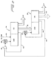
- the present invention replaces the single PLA 22 of Figure 1 with a mainline PLA 34 interconnected with at least one other PLA, such as a subroutine PLA 36.
- a mainline PLA 34 interconnected with at least one other PLA, such as a subroutine PLA 36.
- Each of the PLAs shown in Figure 2 has an AND array and an OR array, and each of the PLAs has its own corresponding sequence counter -- sequence counter 38 for PLA 34 and sequence counter 40 for PLA 36.
- Mainline PLA 34 is incremented by a control bit from its OR array, shown routed by bus 42, to sequence counter 38 and fed as an input to the AND array.
- Mainline PLA 34 is also being incremented, by a control bit from subroutine PLA 36, more specifically, from the OR array thereof and fed via line 44 to sequence counter 38.
- the control bits from the respective OR arrays of PLAs 34 and 36 are gated by an OR gate 43, before being fed to sequence counter 38.
- Subroutine PLA 36 is incremented, via sequence counter 40, by a control bit from its OR array sent through line 46.
- a plural-bit encode number (in the form of plural-bits), sent from the OR array of mainline PLA 34 via bus 48, is also used to address subroutine PLA 36.
- Each of the OR arrays of the respective PLAs has an additional output, designated CP, for providing control points as output signals to perform particular function(s) associated with a given operation code.
- Such an operation code can be seen as being input to the AND array of mainlines PLA 34 from line 50.
- a bus 52 which may be used to provide data bits representing the encode numbers from subroutine PLA 36 to other subroutine PLAs. This nested feature of one subroutine PLA being connected to another will be discussed later in this application.
- an automatic branch for performing different operations, may be effected with the same operation code.
- an operation code were to have generated a sequence of different microwords (for corresponding functions), as was sequentially done by the same PLA in the prior art, the present invention can actually use a single PLA for generating individually each of the microwords. And when the corresponding functions are done, a branching back from the subroutine PLA(s) to the mainline PLA is automatically effected.
- the subroutine PLA may be used repeatedly to perform the same function such that each time that function is finished, an automatic branching back to the part of the processor instruction which requires the execution of that particular function can be effected, without having to have special hardware or having to actually execute the same processor instruction repeatedly.
- the embodiment of Figure 2 is executing a "firmware" subroutining, which is much less expensive than software subroutining, conventional circuitries or read only storage (ROS), which are much more expensive than PLAs, ie. they have greater power consumption and there is more silicon or "real-estate” required, and also require more real estate in the data processor.
- firmware firmware subroutining
- PLAs read only storage
- the OR array of mainline PLA 34 contains a two bit encode number that is fed, via bus 48, to the AND array of subroutine PLA 36.
- a two bit encode number field is used, it should be appreciated that an encode number containing as many bits as necessary can also be used, as the encode number field can be expanded to accommodate the additional bits.
- the encode number field is designated as 54 and 56 in the OR array of mainline PLA 34 and the AND array of subroutine PLA 36, respectively.
- the respective sequence counters 38 and 40 are shown to increment only three bits in the respective AND arrays. As before, a much greater number of data bits can be accommodated in the respective AND arrays.
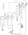
- a plurality of states are located within the AND array (AND partition) of mainline PLA 34.
- the respective states are referred to as states 0, 1, 2, etc., as shown to the left of the AND array.
- Each of the states is comprised of a set of data bits. For example, state 0 is represented by 000 while state 2 is represented by 010.
- Each state in the AND array has a corresponding set of data bits in the OR array (OR partition).
- this set of data bits is comprised of only the bits representative of the encode numbers and an incrementing bit, which is shown as being output to sequence counter 38, by means of line 42.
- state 0 is represented as 001 in the OR array of PLA 34.
- Each state of the AND array of subroutine PLA 36 in addition to the data bits representing the sequence count, further has data bits representing the encode number for subroutine PLA 36 which is limited to two data bits since only two data bits are represented in the OR array of mainline PLA 34.
- subroutine PLA 36 is shown to have an encode number represented by data bits having values 10.
- state 0 is represented by 10000 while state 2 is represented by 10010.
- the set of data bits in its AND array has a corresponding set of data bits in its OR array.
- each pair of corresponding set of data bits in the OR array of subroutine PLA 36 is shown to have only two data bits -- one being used to increment mainline PLA 34 while the other being used to increment subroutine PLA 36.
- the OR array of subroutine PLA 36 also has a plurality of sets of control points, not shown, for performing particular functions.
- Figure 3 operates as follows. Assume that sequence counters 38 and 40 have been reset to 000, i.e. the initial state, and that the operation code (not shown in Figure 3) has chosen a value of 010 ( i.e. state 2) for producing the function it requires. As mainline PLA 34 is sequenced by sequence counter 38, by means of the incrementing control data bit having the value of 1 through line 42, nothing happens during the first two states 0 and 1, as the encode number bits have values of 00. However, when mainline PLA 34 is incremented to state 2 (010), the encode number field has a corresponding set of data bits having the value 10, which as can be seen, corresponds to the data bit values in encode number field 56 in the AND array of subroutine PLA 36.
- subroutine PLA 36 is activated.
- the incrementing control data bit in the OR array of mainline PLA 34 has a value of 0. This signifies the effective freezing, or suspension, of operation of mainline PLA 34.
- mainline PLA 34 is suspended in state 2, as subroutine PLA 36 takes over the operation. It is important to note, however, that even though mainline PLA 34 is effectively suspended, data bits representing control points for state 2 are still being output from its OR array.
- subroutine PLA 36 When the value of encode number field 56 of subroutine PLA 36 matches that of encode number field 54 at state 2 (010) of mainline PLA 34, subroutine PLA 36 is incremented, by means of its subroutine sequence counter control point which has a value 1, and carried along line 46 to sequence counter 40. As subroutine PLA 36 sequences through its states, in this instance states 0 to 3, it is, of course, generating control point signals from its OR array for performing specific functions.
- sequence counter 38 is activated for stepping mainline PLA 34 from state 2 to state 3, i.e. from 010 to 011. Since encode number field 54 for state 3 now has a value 00, subroutine PLA 36 no longer is "addressed.” Hence, an automatic branching from subroutine PLA 36 back to mainline PLA 34 is effected.
- sequence counter 40 of subroutine PLA 36 can be reset to 0 in order to prepare for the next subroutine entry. Or, alternatively, it can be left as is, or set to some other state, if a particular function is desired when it next operates.
- each PLA has to have its own corresponding sequence counter; each PLA must have a control point in its OR array to increment its own sequence counter and must also have a control point to increment the sequence counter of the PLA that feeds it; and each PLA has to have an encode number field in its OR array that is used to form part of an "address" to the PLA that it is feeding, so that when the data bits in the encode number field of the fed PLA match the data bits of the encode number field of the feeding PLA, the fed PLA becomes operative.
- a plurality of PLAs may become operative at the same time.
- subroutine PLA 36 and subroutine PLA 60 could be operating at the same time to execute different functions required by the operation code.
- subroutine PLA 36 may still be sequencing, and thereby operating, while subroutine PLA 60 may already have been incremented to a state whereby it is suspended and control has been passed on to second level subroutine PLA 64.
- the expected control point signals from these "suspended" PLAs (which may also include those of mainline PLA 34) can be combined with the control points output from the "operative" PLAs.
- the present invention allows the simultaneous generation of each microword of a sequence of microwords. Flexible and efficient operations result from the feature which allows a fed PLA to automatically branch back to a feeding PLA.
- LSSD Level Sensitive Scan Design
- LSSD mechanism uses two latches L1 and L2 which together represent one bit of a sequence counter.
- An output from the OR array (of the feeding PLA) is latched into the L1 latch via a " ⁇ 1 " clock.
- a subsequent " ⁇ 2 " clock transfers the latch information from latch L1 to latch L2, thereby causing a change in the output of the OR array, which is again latched into the L 1 latch.
- the output of the OR array can actually be clocked while the particular data is read out, even though the address (state) has been incremented. Putting it differently, the data bit values of the state will not be changed until " ⁇ 2 " clock comes along.
- the " ⁇ 1 " clock and the “ ⁇ 2 " clock are two mutually exclusive clocks and are separated by an increment of time for providing this so-called “non- overlaying mode", which is necessary inasmuch as it is desireable to insure that no logical race conditions occur as the feeding PLA is being incremented by a control point from a fed subroutine PLA.
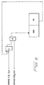
- Figure 6 illustrates an arrangement whereby a subroutine PLA can recursively operate. This is accomplished by including a subroutine encode number field in the OR array of the subroutine PLA.
- a data bit representing the subroutine enable data bit may be fed from line 66 to latches 68 for gating with the data bits from the encode number field of the feeding PLA which, in the embodiment of Figure 6, is shown as a mainline PLA.
- the subroutine enable data bit field can be shared with an existing control field if the function that it is to be shared with is mutually exclusive. As can be seen, a small amount of control logic is required in order to distinguish the logical meaning of this field on a time-share basis.
- a plurality of latching arrangements as shown in Figure 5 have been incorporated into the embodiment of Figure 6.
- sequence counter controls are not shown.
- an automatic branching to different places within the same physical subroutine PLA can be effected.
- this recursive arrangement is desirable inasmuch as a particular function has to be repeated a number of times.
- the subroutine enabled data bit is given a non-enabling value.
Claims (3)
- Appareil de commande à microcode pour un processeur de données dans lequel des micromots sont utilisés pour effectuer l'exécution des instructions du processeur, l'appareil comprenant:un premier PLA (34) ayant une séparation d'entrée contenant une pluralité d'états pour recevoir un code d'opération d'une instruction du processeur, un moyen de séquencement (38) pour incrémenter les états de la séparation d'entrée, et une séparation de sortie pour générer des séries de sortie de bits de données (42, 48, CP) correspondant au nombre d'états présents dans la séparation d'entrée;au moins un second PLA (36) ayant une séparation de sortie contenant une pluralité d'états pour recevoir une série de bits de données à partir de la séparation de sortie du premier PLA (34), un moyen de séquencement (40) pour incrémenter les états de la séparation d'entrée, et une séparation de sortie pour générer des séries de sortie de bits de données correspondant au nombre d'états présents dans la séparation d'entrée;dans lequel au moins une partie prédéfinie (48) des séries de sortie de bits de données du premier PLA (34) est utilisée comme entrée pour la séparation d'entrée du second PLA (36), le second PLA (36) étant agencé de telle sorte que son fonctionnemnet soit amorcé lorsque ladite partie prédéfinie des séries de sortie de bits de données du premier PLA (36) correspond à un numéro de code prédéfini,la séparation de sortie du second PLA (36) utilisant au moins un signal de commande, correspondant à un micromot, pour effectuer une fonction nécessitée par le code opérationnel,caractérisé par une porte OU (43) directement connectée aux parties de sortie respectives (42, 44) des premier et second PLA et agencée pour incrémenter le moyen de séquencement (38) du premier PLA (34) lorsque soit au moins l'un des bits de sortie (44) du second PLA (36) soit au moins un bit de la sortie (42) du premier PLA (34) est une valeur prédéterminée de deux valeurs,et en ce qu'un autre des bits de sortie (46) du second PLA (36) est effectif pour incrémenter le moyen de séquencement (40) du second PLA (36) à l'une prédéterminée de deux valeurs,les états de sortie du premier PLA (34) étant tels que leur sortie n'est pas effective pour incrémenter le premier PLA (34) lorsque la partie prédéfinie des séries de bits de données dans la séparation de sortie du premier PLA (34) correspond au nombre de code prédéfini et les états de sortie du second PLA (36) étant tels qu'une fois amorcé le second PLA (36) reste opérationnel jusqu'à ce que sa sortie soit effective pour l'incrémenter (46) n'est plus à ladite valeur et de telle sorte que sa sortie (44) effective pour incrémenter le premier PLA (34) soit ensuite à ladite valeur pour effectuer l'incrémentation du premier PLA (34), un rebranchement automatique au premier PLA (34) à partir du second PLA (36) résultant de celui-ci.
- Appareil selon la revendication 1, comprenant au moins un troisième PLA (62) ayant une séparation d'entrée contenant une pluralité d'états pour recevoir une série de bits de données en provenance de la séparation de sortie du second PLA (36), un moyen de séquencement pour incrémenter les états de la séparation d'entrée, et une séparation de sortie pour générer des séries de sortie de bits de données correspondant au nombre d'états présents dans la séparation d'entrée;dans lequel au moins une partie prédéfinie des séries de sortie de bits de données du second PLA (36) est utilisée comme entrée pour la séparation d'entrée du troisième PLA (62), le troisième PLA (62) étant agencé de telle sorte que son fonctionnement soit amorcé lorsque ladite partie prédéfinie des séries de sortie de bits de données du second PLA (36) correspond à un nombre de code prédéfini,la séparation de sortie du troisième PLA (62) utilisant au moins un signal de commande, correspondant à un micromot, pour effectuer une fonction nécessitée par le code d'opération,et une porte OU directement connectée aux parties de sortie respectives des second et troisième PLA et agencée pour incrémenter le moyen de séquencement (40) du second PLA (36) lorsque soit au moins l'un des bits de sortie du troisième PLA (62) soit au moins un bit de la sortie du second PLA (36) est à une valeur prédéterminée parmi les deux valeurs,et en ce qu'un autre des bits de sortie du troisième PLA (62) est effectif pour incrémenter le moyen de séquencement du troisième PLA (62) à une valeur prédéterminée parmi deux valeurs,les états de sortie du second PLA (36) étant tels que sa sortie n'est pas effective pour incrémenter le second PLA (36) lorsque la partie prédéfinie des séries de bits de données dans la séparation de sortie du second PLA (36) correspond au nombre de code prédéfini et les états de sortie du troisième PLA (62) étant telle que une fois amorcé le troisième PLA (62) reste opérationnel jusqu'à ce que sa sortie effective pour l'incrémenter n'est plus à ladite valeur et de telle sorte que sa sortie effective pour incrémenter le second PLA (36) soit ensuite à ladite valeur pour effectuer l'incrémentation du second PLA (36), un rebranchement automatique au second PLA (36) à partir du troisième PLA (62) résultant de celle-ci.
- Processeur de données comportant l'appareil de commande de microcode selon la revendication 1 ou la revendication 2.
Applications Claiming Priority (2)
| Application Number | Priority Date | Filing Date | Title |
|---|---|---|---|
| US296168 | 1989-01-12 | ||
| US07/296,168 US5043879A (en) | 1989-01-12 | 1989-01-12 | PLA microcode controller |
Publications (3)
| Publication Number | Publication Date |
|---|---|
| EP0377976A2 EP0377976A2 (fr) | 1990-07-18 |
| EP0377976A3 EP0377976A3 (fr) | 1993-01-27 |
| EP0377976B1 true EP0377976B1 (fr) | 1996-07-17 |
Family
ID=23140895
Family Applications (1)
| Application Number | Title | Priority Date | Filing Date |
|---|---|---|---|
| EP89313061A Expired - Lifetime EP0377976B1 (fr) | 1989-01-12 | 1989-12-13 | Dispositif de commande microprogrammé utilisant des circuits à réseaux logiques programmables |
Country Status (5)
| Country | Link |
|---|---|
| US (1) | US5043879A (fr) |
| EP (1) | EP0377976B1 (fr) |
| JP (1) | JPH02226423A (fr) |
| CA (1) | CA2006243C (fr) |
| DE (1) | DE68926851D1 (fr) |
Families Citing this family (16)
| Publication number | Priority date | Publication date | Assignee | Title |
|---|---|---|---|---|
| US5680600A (en) * | 1989-10-13 | 1997-10-21 | Texas Instruments Incorporated | Electronic circuit for reducing controller memory requirements |
| US5189628A (en) * | 1991-03-11 | 1993-02-23 | National Semiconductor Corporation | System and method for partitioning PLA product terms into distinct logical groups |
| US5369772A (en) * | 1992-05-21 | 1994-11-29 | Compaq Computer Corporation | Method of maximizing data pin usage utilizing post-buffer feedback |
| US5440740A (en) * | 1992-10-13 | 1995-08-08 | Chen; Fetchi | System and method for managing devices on multiple digital signal processors |
| JP3068382B2 (ja) * | 1993-09-29 | 2000-07-24 | 株式会社東芝 | プログラマブルロジックアレイ |
| DE19651075A1 (de) * | 1996-12-09 | 1998-06-10 | Pact Inf Tech Gmbh | Einheit zur Verarbeitung von numerischen und logischen Operationen, zum Einsatz in Prozessoren (CPU's), Mehrrechnersystemen, Datenflußprozessoren (DFP's), digitalen Signal Prozessoren (DSP's) oder dergleichen |
| US5854922A (en) * | 1997-01-16 | 1998-12-29 | Ford Motor Company | Micro-sequencer apparatus and method of combination state machine and instruction memory |
| US6542998B1 (en) | 1997-02-08 | 2003-04-01 | Pact Gmbh | Method of self-synchronization of configurable elements of a programmable module |
| US6163836A (en) * | 1997-08-01 | 2000-12-19 | Micron Technology, Inc. | Processor with programmable addressing modes |
| US8058899B2 (en) | 2000-10-06 | 2011-11-15 | Martin Vorbach | Logic cell array and bus system |
| US7444531B2 (en) | 2001-03-05 | 2008-10-28 | Pact Xpp Technologies Ag | Methods and devices for treating and processing data |
| US9037807B2 (en) | 2001-03-05 | 2015-05-19 | Pact Xpp Technologies Ag | Processor arrangement on a chip including data processing, memory, and interface elements |
| US7996827B2 (en) | 2001-08-16 | 2011-08-09 | Martin Vorbach | Method for the translation of programs for reconfigurable architectures |
| US20040268104A1 (en) * | 2001-10-01 | 2004-12-30 | Cooper Benjamin Jonathon | General purpose fixed instruction set (fis) bit-slice feedback processor unit/computer system |
| US8914590B2 (en) | 2002-08-07 | 2014-12-16 | Pact Xpp Technologies Ag | Data processing method and device |
| US7693257B2 (en) | 2006-06-29 | 2010-04-06 | Accuray Incorporated | Treatment delivery optimization |
Family Cites Families (32)
| Publication number | Priority date | Publication date | Assignee | Title |
|---|---|---|---|---|
| US3651482A (en) * | 1968-04-03 | 1972-03-21 | Honeywell Inc | Interlocking data subprocessors |
| US3614740A (en) * | 1970-03-23 | 1971-10-19 | Digital Equipment Corp | Data processing system with circuits for transferring between operating routines, interruption routines and subroutines |
| US3794980A (en) * | 1971-04-21 | 1974-02-26 | Cogar Corp | Apparatus and method for controlling sequential execution of instructions and nesting of subroutines in a data processor |
| US3736567A (en) * | 1971-09-08 | 1973-05-29 | Bunker Ramo | Program sequence control |
| US3949370A (en) * | 1974-06-06 | 1976-04-06 | National Semiconductor Corporation | Programmable logic array control section for data processing system |
| US3959774A (en) * | 1974-07-25 | 1976-05-25 | California Institute Of Technology | Processor which sequences externally of a central processor |
| DE2617485C3 (de) * | 1976-04-22 | 1980-09-18 | Nixdorf Computer Ag, 4790 Paderborn | Schaltungsanordnung für Datenverarbeitungsanlagen zur Abarbeitung von Mikrobefehlsfolgen |
| DE2657404B2 (de) * | 1976-12-17 | 1978-09-28 | Siemens Ag, 1000 Berlin Und 8000 Muenchen | Steuerwerk |
| FR2388344A1 (fr) * | 1977-04-19 | 1978-11-17 | Cii Honeywell Bull | Procede et dispositif de calcul d'adresse d'enchainement des micro-instructions a executer dans une memoire de commande d'un systeme informatique |
| US4371931A (en) * | 1979-06-27 | 1983-02-01 | Burroughs Corporation | Linear micro-sequencer for micro-processor system utilizing specialized instruction format |
| US4323963A (en) * | 1979-07-13 | 1982-04-06 | Rca Corporation | Hardware interpretive mode microprocessor |
| US4394736A (en) * | 1980-02-11 | 1983-07-19 | Data General Corporation | Data processing system utilizing a unique two-level microcoding technique for forming microinstructions |
| US4398244A (en) * | 1980-05-07 | 1983-08-09 | Fairchild Camera & Instrument Corporation | Interruptible microprogram sequencing unit and microprogrammed apparatus utilizing same |
| US4438492A (en) * | 1980-08-01 | 1984-03-20 | Advanced Micro Devices, Inc. | Interruptable microprogram controller for microcomputer systems |
| JPS5757345A (en) * | 1980-09-24 | 1982-04-06 | Toshiba Corp | Data controller |
| US4399505A (en) * | 1981-02-06 | 1983-08-16 | Data General Corporaton | External microcode operation in a multi-level microprocessor |
| US4399516A (en) * | 1981-02-10 | 1983-08-16 | Bell Telephone Laboratories, Incorporated | Stored-program control machine |
| US4450525A (en) * | 1981-12-07 | 1984-05-22 | Ibm Corporation | Control unit for a functional processor |
| US4685080A (en) * | 1982-02-22 | 1987-08-04 | International Business Machines Corp. | Microword generation mechanism utilizing separate programmable logic arrays for first and second microwords |
| US4509114A (en) * | 1982-02-22 | 1985-04-02 | International Business Machines Corporation | Microword control mechanism utilizing a programmable logic array and a sequence counter |
| US4594661A (en) * | 1982-02-22 | 1986-06-10 | International Business Machines Corp. | Microword control system utilizing multiplexed programmable logic arrays |
| US4556938A (en) * | 1982-02-22 | 1985-12-03 | International Business Machines Corp. | Microcode control mechanism utilizing programmable microcode repeat counter |
| US4575794A (en) * | 1982-02-22 | 1986-03-11 | International Business Machines Corp. | Clocking mechanism for multiple overlapped dynamic programmable logic arrays used in a digital control unit |
| US4493029A (en) * | 1982-05-14 | 1985-01-08 | At&T Bell Laboratories | Microprocessor with PLA adapted to implement subroutines |
| US4504904A (en) * | 1982-06-15 | 1985-03-12 | International Business Machines Corporation | Binary logic structure employing programmable logic arrays and useful in microword generation apparatus |
| US4546431A (en) * | 1982-11-03 | 1985-10-08 | Burroughs Corporation | Multiple control stores in a pipelined microcontroller for handling jump and return subroutines |
| US4551798A (en) * | 1982-11-03 | 1985-11-05 | Burroughs Corporation | Multiple control stores in a pipelined microcontroller for handling nester subroutines |
| US4488227A (en) * | 1982-12-03 | 1984-12-11 | Honeywell Information Systems Inc. | Program counter stacking method and apparatus for nested subroutines and interrupts |
| US4947369A (en) * | 1982-12-23 | 1990-08-07 | International Business Machines Corporation | Microword generation mechanism utilizing a separate branch decision programmable logic array |
| US4562538A (en) * | 1983-05-16 | 1985-12-31 | At&T Bell Laboratories | Microprocessor having decision pointer to process restore position |
| JP2523474B2 (ja) * | 1985-07-29 | 1996-08-07 | 株式会社東芝 | ガス遮断器 |
| JPH0642207B2 (ja) * | 1987-04-21 | 1994-06-01 | 富士電機株式会社 | マルチレベルプログラミング方式 |
-
1989
- 1989-01-12 US US07/296,168 patent/US5043879A/en not_active Expired - Fee Related
- 1989-12-13 DE DE68926851T patent/DE68926851D1/de not_active Expired - Lifetime
- 1989-12-13 EP EP89313061A patent/EP0377976B1/fr not_active Expired - Lifetime
- 1989-12-20 CA CA002006243A patent/CA2006243C/fr not_active Expired - Fee Related
- 1989-12-20 JP JP1328607A patent/JPH02226423A/ja active Pending
Also Published As
| Publication number | Publication date |
|---|---|
| JPH02226423A (ja) | 1990-09-10 |
| CA2006243A1 (fr) | 1990-07-12 |
| EP0377976A3 (fr) | 1993-01-27 |
| CA2006243C (fr) | 1994-03-15 |
| US5043879A (en) | 1991-08-27 |
| DE68926851D1 (de) | 1996-08-22 |
| EP0377976A2 (fr) | 1990-07-18 |
Similar Documents
| Publication | Publication Date | Title |
|---|---|---|
| EP0377976B1 (fr) | Dispositif de commande microprogrammé utilisant des circuits à réseaux logiques programmables | |
| US4984151A (en) | Flexible, next-address generation microprogram sequencer | |
| US5680597A (en) | System with flexible local control for modifying same instruction partially in different processor of a SIMD computer system to execute dissimilar sequences of instructions | |
| EP0315275B1 (fr) | Microcalculateur avec des circuits intégrés flexibles et spécifiques pour l'application | |
| EP0087011B1 (fr) | Mécanisme de commande de microcodes utilisant un compteur programmable de répétition de microcodes | |
| US4079451A (en) | Word, byte and bit indexed addressing in a data processing system | |
| US4037213A (en) | Data processor using a four section instruction format for control of multi-operation functions by a single instruction | |
| US3651482A (en) | Interlocking data subprocessors | |
| KR880001170B1 (ko) | 마이크로 프로세서 | |
| US3943494A (en) | Distributed execution processor | |
| US5455923A (en) | Memory system for loading peripherals on power up | |
| USRE26171E (en) | Multiprocessing computer system | |
| EP0114191B1 (fr) | Système de contrôle à micro-mot utilisant des réseaux à logique programmable chevauchés | |
| US5155819A (en) | Flexible ASIC microcomputer permitting the modular modification of dedicated functions and macroinstructions | |
| US4685080A (en) | Microword generation mechanism utilizing separate programmable logic arrays for first and second microwords | |
| US4285039A (en) | Memory array selection mechanism | |
| IE53180B1 (en) | Stored-program control machine and structures therefor | |
| EP0010197A1 (fr) | Système de traitement de données pour la coopération d'une mémoire principale avec une sectron de contrôle et une sectron de traitement de données | |
| US5034879A (en) | Programmable data path width in a programmable unit having plural levels of subinstruction sets | |
| US3396371A (en) | Controller for data processing system | |
| US4975837A (en) | Programmable unit having plural levels of subinstruction sets where a portion of the lower level is embedded in the code stream of the upper level of the subinstruction sets | |
| US8200943B2 (en) | Microprocessor | |
| US4931989A (en) | Microword generation mechanism utilizing a separate programmable logic array for first microwords | |
| KR960013358B1 (ko) | 비트 슬라이스 프로세서용 레지스터 파일 | |
| EP0177268B1 (fr) | Largeur de bus de données programmable dans une unité programmable à plusieurs niveaux de jeux de sub-instructions |
Legal Events
| Date | Code | Title | Description |
|---|---|---|---|
| PUAI | Public reference made under article 153(3) epc to a published international application that has entered the european phase |
Free format text: ORIGINAL CODE: 0009012 |
|
| AK | Designated contracting states |
Kind code of ref document: A2 Designated state(s): DE FR GB |
|
| 17P | Request for examination filed |
Effective date: 19901113 |
|
| PUAL | Search report despatched |
Free format text: ORIGINAL CODE: 0009013 |
|
| AK | Designated contracting states |
Kind code of ref document: A3 Designated state(s): DE FR GB |
|
| 17Q | First examination report despatched |
Effective date: 19950111 |
|
| GRAH | Despatch of communication of intention to grant a patent |
Free format text: ORIGINAL CODE: EPIDOS IGRA |
|
| GRAH | Despatch of communication of intention to grant a patent |
Free format text: ORIGINAL CODE: EPIDOS IGRA |
|
| GRAA | (expected) grant |
Free format text: ORIGINAL CODE: 0009210 |
|
| AK | Designated contracting states |
Kind code of ref document: B1 Designated state(s): DE FR GB |
|
| PG25 | Lapsed in a contracting state [announced via postgrant information from national office to epo] |
Ref country code: FR Effective date: 19960717 |
|
| REF | Corresponds to: |
Ref document number: 68926851 Country of ref document: DE Date of ref document: 19960822 |
|
| PG25 | Lapsed in a contracting state [announced via postgrant information from national office to epo] |
Ref country code: DE Effective date: 19961018 |
|
| EN | Fr: translation not filed | ||
| PG25 | Lapsed in a contracting state [announced via postgrant information from national office to epo] |
Ref country code: GB Effective date: 19961213 |
|
| PLBE | No opposition filed within time limit |
Free format text: ORIGINAL CODE: 0009261 |
|
| STAA | Information on the status of an ep patent application or granted ep patent |
Free format text: STATUS: NO OPPOSITION FILED WITHIN TIME LIMIT |
|
| 26N | No opposition filed | ||
| GBPC | Gb: european patent ceased through non-payment of renewal fee |
Effective date: 19961213 |