EP0376397B1 - Einrichtung zur Nachrichtenübertragung unter Verwendung einer Frequenzmodulation - Google Patents
Einrichtung zur Nachrichtenübertragung unter Verwendung einer Frequenzmodulation Download PDFInfo
- Publication number
- EP0376397B1 EP0376397B1 EP89203276A EP89203276A EP0376397B1 EP 0376397 B1 EP0376397 B1 EP 0376397B1 EP 89203276 A EP89203276 A EP 89203276A EP 89203276 A EP89203276 A EP 89203276A EP 0376397 B1 EP0376397 B1 EP 0376397B1
- Authority
- EP
- European Patent Office
- Prior art keywords
- information
- circuit
- signal
- control
- signals
- Prior art date
- Legal status (The legal status is an assumption and is not a legal conclusion. Google has not performed a legal analysis and makes no representation as to the accuracy of the status listed.)
- Expired - Lifetime
Links
- 230000005540 biological transmission Effects 0.000 claims description 20
- 230000001419 dependent effect Effects 0.000 claims 1
- 238000010586 diagram Methods 0.000 description 2
- 238000000034 method Methods 0.000 description 2
- 230000003321 amplification Effects 0.000 description 1
- 230000000694 effects Effects 0.000 description 1
- 238000003199 nucleic acid amplification method Methods 0.000 description 1
- 210000000056 organ Anatomy 0.000 description 1
Images


Classifications
-
- H—ELECTRICITY
- H04—ELECTRIC COMMUNICATION TECHNIQUE
- H04L—TRANSMISSION OF DIGITAL INFORMATION, e.g. TELEGRAPHIC COMMUNICATION
- H04L27/00—Modulated-carrier systems
- H04L27/10—Frequency-modulated carrier systems, i.e. using frequency-shift keying
Definitions
- the present invention provides a device of the kind mentioned in the preamble which avoids any discontinuity in the frequency variations whatever the sequence of binary elements to be transmitted.
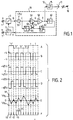
- FIG. 1 represents the diagram of a transmission device according to the invention.
- FIG. 2 shows the appearance of signals present inside the transmission device of FIG. 1.
- FIG. 3 represents the diagram of a reception device according to the invention.
- FIG. 4 shows the appearance of signals present inside the reception device of FIG. 3.
- FIG. 5 shows a transmission device formed by transmission-reception members each consisting of a transmission device and a reception device shown in FIGS. 1 and 3.
- FIG. 1 there is shown a transmission device according to the invention.
- the reference 1 indicates the input terminal to which a signal A is applied representing the data to be transmitted, for example a sequence of "1" and of "0" such as: 1, 0, 0, 0, 1, 1, ... as shown in FIG. 2, line A.
- these data are coded in biphase code by the coder 3 using a signal F coming from a doubler of frequency 5 which doubles the frequency of the clock signals H applied to the terminal 7, accompanying the data to terminal A.
- the biphase code thus formed is represented at B in FIG. 2. This signal changes from -V to + V volts. Each of these values will be transmitted by a frequency modulation of different slope.
- the signals B are applied to a frequency control circuit 10 which acts, as a function of the signals B, on the control 12 of an oscillator 15 whose frequency varies as a function of the voltage applied to its control 12.
- An antenna 17 transmits in space, a wave 18 developed from the oscillator 15.
- the reception device comprises a reception antenna 20 for picking up the wave 18 so that a reception circuit 22 can generate a signal that is easy to demodulate.
- This circuit operates a frequency change obtained by a mixer 25 and an oscillator 27 and an intermediate frequency amplification provided by an amplifier 29.
- the output signals R of this circuit 22 are applied to a demodulator circuit 35 which provides, from a On the other hand, the demodulated signals at an output terminal 37 and the clock signals corresponding to these demodulated signals at terminal 38.
- the control circuit includes means for changing the slope sign constituted by a programmable amplifier 50 whose gain can take two values +1 and -1 depending of a logic signal "1" and "0" respectively, applied to its programming input 51.
- the input of this amplifier receives a signal C from a summing circuit 55 which adds a voltage (1/5) V to the signal B.
- the signal D at the output of the amplifier 50 is applied to an integrating circuit 58 which supplies a signal E towards the frequency control 12 of the oscillator 15.
- This signal is a voltage Vf which varies from -Vf a to + Vf b volts.
- the signal E is also applied to the input of a threshold circuit 60 which supplies a logic signal "0" at its output for a negative voltage applied to its input and a logic signal "1" for a positive or zero voltage.
- a D flip-flop 62 receives on its data input the signal supplied by the circuit 60 and on its clock input the signal F.
- the output signal of this flip-flop is applied to the programming input 51 of the amplifier 50 by means of an EXCLUSIVE gate 63 which receives a signal from a second threshold circuit 64 whose input receives the signal C.
- This threshold circuit 64 provides a logic signal "0” for a voltage negative applied to its input and a signal "1" for a positive or zero voltage.
- the summing circuit 55 By means of the summing circuit 55, the levels of (1/5) V are shifted so that when the signal B is equal to + V the signal C is equal to (6/5) V and when the signal B is equal to -V, signal C is equal to - (4/5) V.
- the choice of the sign + or of the sign - depends in particular on the signal applied to the command 51 and k is a proportionality constant.
- FIG 3 there is shown schematically the structure of the demodulator circuit 35. It consists of a delay line 100 to delay the signal R by ⁇ at the output of the circuit 22. A mixer 102 performs the mixing of the signals R and S (at the output of the line 100).
- FIG. 4b shows the frequency variations of the signal T in correspondence.
- a conventional FSK receiver 105 connected to the output of the mixer 102 restores the data at terminal 37 and the clock signal at terminal 38.
- FIG. 5 shows a transmission device in which each transceiver operates in alternation.
- two transmission-reception members 200 and 201 of identical structure. Only the member 200 is shown in detail.
- As regards its transmission part it is composed of a control circuit 202 with a structure identical to that of circuit 10 receiving data already coded in biphase form.
- the output signal from this circuit 202 is applied to the frequency control of a transmission oscillator 204 by means of a half-time switch 205 placed in the transmission position.
- An antenna 207 radiates in space the wave generated from the output signals from oscillator 204.
- the reception part consists of a reception antenna 210, a mixer 212, an intermediate frequency amplifier 215 and a FSK receiver 220 to restore the data.
- the transmission oscillator 204 also serves as a local oscillator for the reception part.
- a directional coupler 230 takes part of the wave at the output of the oscillator 204 while its frequency control receives a fixed voltage by means of the alternation control placed in the reception position.
Landscapes
- Engineering & Computer Science (AREA)
- Computer Networks & Wireless Communication (AREA)
- Signal Processing (AREA)
- Digital Transmission Methods That Use Modulated Carrier Waves (AREA)
Claims (7)
- Informationsübertragungsanordnung, bei der eine Frequenzmodulation verwendet wird, und welche die nachfolgenden Elemente aufweist:- eine Sendeschaltung, aufgebaut mit einem Oszillator (15) mit einem Frequenzregeleingang (12), zum Senden einer Informationsübertragungswelle,- eine Frequenzregelschaltung (10) zum Liefern von Eingangssignalen zu dem genannten Regeleingang (12) mit Amplituden und mit Neigungen, wobei diese Amplituden und das Vorzeichen der Neigungen von der zu übertragenden Information abhängig ist.dadurch gekennzeichnet, daß die Regelschaltung (10) die nachfolgenden Elemente aufweist:- Mittel (55) zum in Abhängigkeit der zu übertragenden Information Bestimmen des Absolutwertes der neigung der dem genannten Eingang zugeführten Signale,- Mittel (50) zur Änderung des Vorzeichens der Neigung der dem genannten Eingang (12) zugeführten Signale, die außerdem durch Amplitudendetektionsmittel (60) gesteuert werden.
- Informationsübertragungsanordnung nach Anspruch 1, für die der Oszillator (15) von dem spannungsgesteuerten Typ ist, dadurch gekennzeichnet, daß die Detektionsmittel für die Amplituden der Signale, die dem genannten Eingang zugeführt wurden, durch eine Pegeldetektor für die Spannung (60 der genannten Signale gebildet werden.
- Informationsübertragungsanordnung nach Anspruch 2, dadurch gekenn zeichnet, daß die Mittel zur Änderung des Vorzeichens der Neigung der dem genannten Eingang gelieferten Signale durch eine programmierbaren Inverter-Nicht-Inverter (50) gebildet werden zum Umwandeln der Spannungssignale abhängig von den zu übertragenden Daten, wenn die Lage des Inverters-nicht-Inverters der Schaltungsanordnung (50) durch eine Flip-Flop-Schaltung (63) detektiert wird, die im Takte der Informationen den durch den Pegeldetektor (60) gelieferten Wert ladet.
- Informationsempfangsanordnung, die Daten empfängt, die mit Hilfe einer Informationsübertragungsanordnung nach einem der Ansprüche 1 bis 3 gesendet worden sind, dadurch gekennzeichnet, daß diese Schaltungsanordnung die nachfolgenden Elemente aufweist:- eine Empfangsanordnung (22) zum Liefern eines zu demodulierenden Signals,- eine Demodulationsschaltung (35) zum Empfangen des zu demodulierenden Signals mit einer Verzögerungsschaltung (100) zum Verzögern des Signals am Ausgang der Empfangsanordnung und mit einer Mischstufe (102) zum Durchführen der Mischung der Eingangs- und der Ausgangssignale der verzögerungsschaltung,zum Wiederherstellen der Informationen an einer Gebrauchsschaltung.
- Informationsübertragungsanordnung mit mindestens einer Informationssendeanordnung nach einem der Ansprüche 1 bis 3 und mit einer Informationsempfangsanordnung nach Anspruch 4.
- Informationsübertragungsanordnung mit Sende-Empfangsanordnungen, da durch gekennzeichnet, daß jede Sende-Empfangsanordnung aus einer Sendeanordnung nach einem der Ansprüche 1 bis 3 und aus einer Empfangsanordnung nach Anspruch 4 besteht.
- Informationsübertragungsanordnung nach Anspruch 6, dadurch gekenn zeichnet, daß sie eine Wechselregelschaltung aufweist, wodurch wechselweise gesendet und empfangen werden kann.
Applications Claiming Priority (2)
| Application Number | Priority Date | Filing Date | Title |
|---|---|---|---|
| FR8817229A FR2641919B1 (fr) | 1988-12-27 | 1988-12-27 | Dispositif de transmission d'informations utilisant une modulation en frequence |
| FR8817229 | 1988-12-27 |
Publications (2)
| Publication Number | Publication Date |
|---|---|
| EP0376397A1 EP0376397A1 (de) | 1990-07-04 |
| EP0376397B1 true EP0376397B1 (de) | 1995-03-22 |
Family
ID=9373458
Family Applications (1)
| Application Number | Title | Priority Date | Filing Date |
|---|---|---|---|
| EP89203276A Expired - Lifetime EP0376397B1 (de) | 1988-12-27 | 1989-12-20 | Einrichtung zur Nachrichtenübertragung unter Verwendung einer Frequenzmodulation |
Country Status (5)
| Country | Link |
|---|---|
| US (1) | US5073903A (de) |
| EP (1) | EP0376397B1 (de) |
| JP (1) | JPH02222245A (de) |
| DE (1) | DE68921861T2 (de) |
| FR (1) | FR2641919B1 (de) |
Families Citing this family (2)
| Publication number | Priority date | Publication date | Assignee | Title |
|---|---|---|---|---|
| SE510890C2 (sv) * | 1996-08-02 | 1999-07-05 | Ericsson Telefon Ab L M | Förfarande och anordning för bredbandstransmission |
| US8766217B2 (en) * | 2008-05-22 | 2014-07-01 | Vladimir Yegorovich Balakin | Multi-field charged particle cancer therapy method and apparatus |
Family Cites Families (7)
| Publication number | Priority date | Publication date | Assignee | Title |
|---|---|---|---|---|
| US4214208A (en) * | 1963-08-07 | 1980-07-22 | The United States Of America As Represented By The Secretary Of The Army | Jamming of keyed continuous wave radio signals |
| FR1435148A (fr) * | 1965-03-04 | 1966-04-15 | Trt Telecom Radio Electr | Procédé et appareillage de transmission radiotélégraphique au moyen d'impulsions modulées en fréquence |
| US3959601A (en) * | 1975-06-27 | 1976-05-25 | Ford Motor Company | Variable rate clock signal recovery circuit |
| US4438519A (en) * | 1981-05-04 | 1984-03-20 | General Electric Company | Methods, and apparatus, for transmitting high-bit-rate digital data in power line communication media having high harmonic noise content |
| US4468792A (en) * | 1981-09-14 | 1984-08-28 | General Electric Company | Method and apparatus for data transmission using chirped frequency-shift-keying modulation |
| US4606049A (en) * | 1984-12-03 | 1986-08-12 | The United States Of America As Represented By The Secretary Of The Navy | Remote transmitter control system |
| US4849998A (en) * | 1988-06-03 | 1989-07-18 | Communications Satellite Corporation | Rate synchronized symbol timing recovery for variable rate data transmission systems |
-
1988
- 1988-12-27 FR FR8817229A patent/FR2641919B1/fr not_active Expired - Lifetime
-
1989
- 1989-12-18 US US07/452,859 patent/US5073903A/en not_active Expired - Fee Related
- 1989-12-20 EP EP89203276A patent/EP0376397B1/de not_active Expired - Lifetime
- 1989-12-20 DE DE68921861T patent/DE68921861T2/de not_active Expired - Fee Related
- 1989-12-25 JP JP1336190A patent/JPH02222245A/ja active Pending
Also Published As
| Publication number | Publication date |
|---|---|
| DE68921861D1 (de) | 1995-04-27 |
| DE68921861T2 (de) | 1995-11-09 |
| JPH02222245A (ja) | 1990-09-05 |
| FR2641919B1 (fr) | 1991-03-22 |
| FR2641919A1 (fr) | 1990-07-20 |
| US5073903A (en) | 1991-12-17 |
| EP0376397A1 (de) | 1990-07-04 |
Similar Documents
| Publication | Publication Date | Title |
|---|---|---|
| EP0250280B1 (de) | Anordnung für seismische Signaltransmission mittels Radiorelais | |
| EP0629758A1 (de) | Fernbedienungssystem mit mehreren funktionellen Reichweiten ausgewählt auf Grund verschiedener Detektionsschwellen | |
| FR2731853A1 (fr) | Procede et dispositif de demodulation par echantillonnage, notamment pour systeme d'alarme de vehicule automobile | |
| KR100518720B1 (ko) | 차동 위상편이변조 복조장치 | |
| EP0658993B1 (de) | Verfahren und Vorrichtung zur Erkennung von falscher Trägerfrequenzwiedergewinnung und zur Bestimmung des Signal-Rausch-Verhältnisses Eb/No einer digitalen Übertragungsstrecke | |
| EP0561690B1 (de) | Verfahren und Vorrichtung zur Feststellung des Erreichens eines vorausbestimmten Abstandes eines Punktreflektors mittels der Laufzeit einer kontinuierlichen Welle | |
| EP0408112B1 (de) | Pulsradargerät und für den Einbau in dieses Gerät geeignete Pulsdiskriminierungsschaltung | |
| EP0570289B1 (de) | Einrichtung zur Detektion der Durchfahrt eines Fahrzeuges mittels eines passiven Transponders | |
| EP0376397B1 (de) | Einrichtung zur Nachrichtenübertragung unter Verwendung einer Frequenzmodulation | |
| FR2575623A1 (fr) | Appareil de memorisation numerique d'echantillons d'un signal comprenant une composante de frequence porteuse et une composante de modulation angulaire | |
| EP0863408B1 (de) | Geräuschreduzierungsvorrichtung für Radarempfänger | |
| FR2500926A1 (fr) | Dispositif pour transmettre une grandeur mesuree d'un objet mobile a un objet stationnaire par rapport a ce dernier | |
| FR2546630A1 (fr) | Recepteur pour systeme radar doppler a impulsions | |
| FR2793562A1 (fr) | Systeme securise pour la commande du deverrouillage d'au moins un ouvrant de vehicule automobile | |
| EP0538096B1 (de) | Verfahren und Vorrichtung zur Messung von kurzen Abständen durch Analyse der Ausbreitungsverzögerung einer Welle | |
| EP0048200B1 (de) | Abstimmfrequenz-Suchvorrichtung für einen frequenzmodulierten Funkempfänger | |
| EP0097753A1 (de) | Tonempfänger für digitales Datenübertragungssystem | |
| US5528632A (en) | Non-complex dual-correlation phase reversal detector and method | |
| EP1058402B1 (de) | Verfahren zur Verarbeitung eines Impulssignals mit einer adaptiven Schwelle und entsprechender Empfänger | |
| EP0790729B1 (de) | Korrektur von Phasenrauschen einer PLL in einem PSK- oder QAM-Empfänger | |
| FR2621132A1 (fr) | Procede et dispositif de mesures de distances | |
| EP0035434B1 (de) | Sende- und Empfangsvorrichtung zur Übertragung digitaler Signale | |
| EP1759327B1 (de) | Kontaktloses synchronphasendemodulationsverfahren und assoziierter leser | |
| FR2771234A1 (fr) | Systeme et procede de transmission radio | |
| FR2571193A1 (fr) | Emetteur et recepteur de messages constitues d'impulsions successives modulant une porteuse a frequence fixe |
Legal Events
| Date | Code | Title | Description |
|---|---|---|---|
| PUAI | Public reference made under article 153(3) epc to a published international application that has entered the european phase |
Free format text: ORIGINAL CODE: 0009012 |
|
| AK | Designated contracting states |
Kind code of ref document: A1 Designated state(s): DE FR GB IT SE |
|
| 17P | Request for examination filed |
Effective date: 19901219 |
|
| 17Q | First examination report despatched |
Effective date: 19930416 |
|
| GRAA | (expected) grant |
Free format text: ORIGINAL CODE: 0009210 |
|
| AK | Designated contracting states |
Kind code of ref document: B1 Designated state(s): DE FR GB IT SE |
|
| REF | Corresponds to: |
Ref document number: 68921861 Country of ref document: DE Date of ref document: 19950427 |
|
| ITF | It: translation for a ep patent filed | ||
| GBT | Gb: translation of ep patent filed (gb section 77(6)(a)/1977) |
Effective date: 19950619 |
|
| PLBE | No opposition filed within time limit |
Free format text: ORIGINAL CODE: 0009261 |
|
| STAA | Information on the status of an ep patent application or granted ep patent |
Free format text: STATUS: NO OPPOSITION FILED WITHIN TIME LIMIT |
|
| 26N | No opposition filed | ||
| PGFP | Annual fee paid to national office [announced via postgrant information from national office to epo] |
Ref country code: FR Payment date: 19961220 Year of fee payment: 8 |
|
| PGFP | Annual fee paid to national office [announced via postgrant information from national office to epo] |
Ref country code: GB Payment date: 19971201 Year of fee payment: 9 |
|
| PGFP | Annual fee paid to national office [announced via postgrant information from national office to epo] |
Ref country code: SE Payment date: 19971222 Year of fee payment: 9 |
|
| PG25 | Lapsed in a contracting state [announced via postgrant information from national office to epo] |
Ref country code: FR Free format text: THE PATENT HAS BEEN ANNULLED BY A DECISION OF A NATIONAL AUTHORITY Effective date: 19971231 |
|
| PGFP | Annual fee paid to national office [announced via postgrant information from national office to epo] |
Ref country code: DE Payment date: 19980223 Year of fee payment: 9 |
|
| PG25 | Lapsed in a contracting state [announced via postgrant information from national office to epo] |
Ref country code: GB Free format text: LAPSE BECAUSE OF NON-PAYMENT OF DUE FEES Effective date: 19981220 |
|
| PG25 | Lapsed in a contracting state [announced via postgrant information from national office to epo] |
Ref country code: SE Free format text: LAPSE BECAUSE OF NON-PAYMENT OF DUE FEES Effective date: 19981221 |
|
| GBPC | Gb: european patent ceased through non-payment of renewal fee |
Effective date: 19981220 |
|
| PG25 | Lapsed in a contracting state [announced via postgrant information from national office to epo] |
Ref country code: DE Free format text: LAPSE BECAUSE OF NON-PAYMENT OF DUE FEES Effective date: 19991001 |
|
| PG25 | Lapsed in a contracting state [announced via postgrant information from national office to epo] |
Ref country code: IT Free format text: LAPSE BECAUSE OF NON-PAYMENT OF DUE FEES Effective date: 20051220 |