EP0375205A2 - Thermal imaging device - Google Patents
Thermal imaging device Download PDFInfo
- Publication number
- EP0375205A2 EP0375205A2 EP89312730A EP89312730A EP0375205A2 EP 0375205 A2 EP0375205 A2 EP 0375205A2 EP 89312730 A EP89312730 A EP 89312730A EP 89312730 A EP89312730 A EP 89312730A EP 0375205 A2 EP0375205 A2 EP 0375205A2
- Authority
- EP
- European Patent Office
- Prior art keywords
- layer
- array
- electrodes
- infra
- pyroelectric
- Prior art date
- Legal status (The legal status is an assumption and is not a legal conclusion. Google has not performed a legal analysis and makes no representation as to the accuracy of the status listed.)
- Granted
Links
- 238000001931 thermography Methods 0.000 title claims abstract description 12
- 239000000463 material Substances 0.000 claims abstract description 15
- 239000004020 conductor Substances 0.000 claims description 11
- 238000000034 method Methods 0.000 claims description 5
- 238000004519 manufacturing process Methods 0.000 claims description 4
- 238000005530 etching Methods 0.000 claims 2
- BASFCYQUMIYNBI-UHFFFAOYSA-N platinum Chemical compound [Pt] BASFCYQUMIYNBI-UHFFFAOYSA-N 0.000 description 15
- PCHJSUWPFVWCPO-UHFFFAOYSA-N gold Chemical compound [Au] PCHJSUWPFVWCPO-UHFFFAOYSA-N 0.000 description 10
- 229910052737 gold Inorganic materials 0.000 description 10
- 239000010931 gold Substances 0.000 description 10
- 239000004411 aluminium Substances 0.000 description 9
- 229910052782 aluminium Inorganic materials 0.000 description 9
- XAGFODPZIPBFFR-UHFFFAOYSA-N aluminium Chemical compound [Al] XAGFODPZIPBFFR-UHFFFAOYSA-N 0.000 description 9
- 230000005855 radiation Effects 0.000 description 8
- 229910052697 platinum Inorganic materials 0.000 description 4
- QTBSBXVTEAMEQO-UHFFFAOYSA-N Acetic acid Chemical compound CC(O)=O QTBSBXVTEAMEQO-UHFFFAOYSA-N 0.000 description 3
- XUIMIQQOPSSXEZ-UHFFFAOYSA-N Silicon Chemical compound [Si] XUIMIQQOPSSXEZ-UHFFFAOYSA-N 0.000 description 3
- 229910052751 metal Inorganic materials 0.000 description 3
- 239000002184 metal Substances 0.000 description 3
- 229920002120 photoresistant polymer Polymers 0.000 description 3
- 229910052710 silicon Inorganic materials 0.000 description 3
- 239000010703 silicon Substances 0.000 description 3
- 239000004642 Polyimide Substances 0.000 description 2
- 239000006096 absorbing agent Substances 0.000 description 2
- 239000011358 absorbing material Substances 0.000 description 2
- 238000010521 absorption reaction Methods 0.000 description 2
- 239000011810 insulating material Substances 0.000 description 2
- 238000001020 plasma etching Methods 0.000 description 2
- 229920001721 polyimide Polymers 0.000 description 2
- LIVNPJMFVYWSIS-UHFFFAOYSA-N silicon monoxide Chemical compound [Si-]#[O+] LIVNPJMFVYWSIS-UHFFFAOYSA-N 0.000 description 2
- 230000006978 adaptation Effects 0.000 description 1
- 239000003989 dielectric material Substances 0.000 description 1
- 238000012986 modification Methods 0.000 description 1
- 230000004048 modification Effects 0.000 description 1
- 238000000206 photolithography Methods 0.000 description 1
- 229920000642 polymer Polymers 0.000 description 1
- 238000010561 standard procedure Methods 0.000 description 1
- 238000001039 wet etching Methods 0.000 description 1
Images

Classifications
-
- G—PHYSICS
- G01—MEASURING; TESTING
- G01J—MEASUREMENT OF INTENSITY, VELOCITY, SPECTRAL CONTENT, POLARISATION, PHASE OR PULSE CHARACTERISTICS OF INFRARED, VISIBLE OR ULTRAVIOLET LIGHT; COLORIMETRY; RADIATION PYROMETRY
- G01J5/00—Radiation pyrometry, e.g. infrared or optical thermometry
- G01J5/10—Radiation pyrometry, e.g. infrared or optical thermometry using electric radiation detectors
- G01J5/34—Radiation pyrometry, e.g. infrared or optical thermometry using electric radiation detectors using capacitors, e.g. pyroelectric capacitors
-
- H—ELECTRICITY
- H10—SEMICONDUCTOR DEVICES; ELECTRIC SOLID-STATE DEVICES NOT OTHERWISE PROVIDED FOR
- H10N—ELECTRIC SOLID-STATE DEVICES NOT OTHERWISE PROVIDED FOR
- H10N15/00—Thermoelectric devices without a junction of dissimilar materials; Thermomagnetic devices, e.g. using the Nernst-Ettingshausen effect
- H10N15/10—Thermoelectric devices using thermal change of the dielectric constant, e.g. working above and below the Curie point
-
- G—PHYSICS
- G01—MEASURING; TESTING
- G01J—MEASUREMENT OF INTENSITY, VELOCITY, SPECTRAL CONTENT, POLARISATION, PHASE OR PULSE CHARACTERISTICS OF INFRARED, VISIBLE OR ULTRAVIOLET LIGHT; COLORIMETRY; RADIATION PYROMETRY
- G01J5/00—Radiation pyrometry, e.g. infrared or optical thermometry
- G01J5/10—Radiation pyrometry, e.g. infrared or optical thermometry using electric radiation detectors
- G01J5/34—Radiation pyrometry, e.g. infrared or optical thermometry using electric radiation detectors using capacitors, e.g. pyroelectric capacitors
- G01J2005/345—Arrays
-
- H—ELECTRICITY
- H04—ELECTRIC COMMUNICATION TECHNIQUE
- H04N—PICTORIAL COMMUNICATION, e.g. TELEVISION
- H04N5/00—Details of television systems
- H04N5/30—Transforming light or analogous information into electric information
- H04N5/33—Transforming infrared radiation
Definitions
- This invention relates to thermal imaging devices and in particular to thermal imaging devices comprising an array of pyroelectric detector elements responsive to infra-red radiation.
- the main factor limiting the performance of existing thermal imaging devices is the thermal conductance between adjacent detector elements and between each detector element and the supporting and interrogating structure.
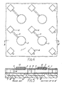
- a pyroelectric film 1 has an array of interconnected electrodes 2 formed on one side and an array of discrete electrodes 3 formed on the other side. Electrically conductive pads 4 are connected by long thin conductors 5 to the discrete electrodes 3 and by electrically conductive pillars 6 to input pads 7 of an integrated signal processing circuit located adjacent to the input pads of electrical circuits formed in regions 8 of a silicon wafer 9. The input pads 7 are separated by regions 10 of a passivating layer of an insulating material, for example silicon monoxide.
- each discrete electrode 3, as best seen in Figure 1 is square shaped with a central gap 11 in which the pad 4 lies.
- the long, narrow conductor 5 extends around the pad 4 within the gap 11.
- the interconnected electrodes 2, as best seen in Figure 2 each have a central hole 12 corresponding to the gap 11 in the respective discrete electrode 3 and may carry an infra-red absorption layer 13, consisting of, for example, black gold, platinum black or a metal-dielectric-metal sandwich structure.
- the discrete electrodes 3 are spaced from respective electrically conductive pads 4 and connected to them by long narrow conductors 5.
- the pillars are attached to respective electrically conductive pads 4, each of which lies centrally disposed with respect to several (in the case illustrated four) adjacent discrete electrodes 3.
- the interconnected electrodes 2 are in positions corresponding to the discrete electrodes 3 and again carry an appropriate infra-red absorption layer 13.
- Both arrangements shown in Figures 1 to 5 provide a low, thermal conductance from the active areas of the discrete electrodes 3 to the pillars 6 because the electrical connection between the electrodes 3 and pillars 6 includes the long narrow conductor 5.
- both arrangements involve significant areas either within (in the device illustrated in Figures 1-3) or around (in the device illustrated in Figures 4 and 5) the discrete electrodes 3 where the incident radiation is wasted and consequently the signal to noise ratio of the device is reduced.
- the discrete electrodes 3 could be brought closer together by meandering the conductor 5, as proposed inEuropean Patent Application No. 89305496 but there would still be significant incident radiation wasted at and around the pads 4.
- a thermal imaging device comprises: a layer comprising pyroelectric material; an array of interconnected electrodes carried on one major surface of the layer; an array of discrete electrodes carried on the other major surface of the layer so as to define with the interconnected electrodes an array of pyroelectric detector elements; a plurality of pillars effective to support the layer, and to enable the passage of electrical signals between the detector element and an electrical signal processing means, each pillar being electrically connected to a discrete electrode by an elongate strip of electrically conductive material which extends over a region of the layer which carries no electrodes, the device being characterised in that said one major surface of the layer carries areas of infra-red absorbant material which extend into said regions carrying no electrodes, said areas being effective to conduct heat from each region to the adjacent pyroelectric detector element.
- the areas of infra-red absorbant material suitably comprise extensions of the interconnected electrodes arranged to overhang said regions out of electrical contact with the regions.
- the interconnected electrodes and their extensions preferably carry infra-red absorbing layers.
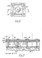
- a pyroelectric film 31 has an array of interconnected gold electrodes 32 formed on one side and an array of discrete gold electrodes 33 on the other side. Electrically conductive pads 34 are connected by long, thin, coiled conductors to the discrete electrodes 33 and by electrically conductive pillars 36 to input pads 37 of integrated signal processing circuits 38 formed within adjacent regions of a silicon wafer 39. The input pads 37 are separated by regions of a passivating layer 40 of an insulating material carried on the wafer 39.
- the discrete electrodes 33 are constructed in equivalent manner to those shown in Figure 1, described hereinbefore.
- the interconnected electrodes 32 differ from those shown in Figures 2 and 3 in that they have extensions 32a which extend over regions of the pyroelectric film 31 carrying the coiled conductors 35 on the other major surface.
- the extension 32a are spaced from the surface of the pyroelectric film, such that the extensions resemble domes as can be seen in Figures 6 and 7. These domes have a central small hole 41 to facilitate fabrication, as will be explained hereafter.
- the interconnected electrodes 32, together with the extensions 32a carry a layer 42 of an infra-red absorbing material, such as platinum black carried on a platinum layer 43 or any other suitable infra-red absorber such as black gold or a metal-dielectric-metal sandwich structure.
- dome-shaped extensions 32a with their overlying infra-red absorbing layers will intercept radiation in the regions around the pillars carrying the conductors 35, which would otherwise be wasted.
- the thermal leakage from the absorber to the non-active i.e. non-electroded areas of the pyroelectric material is minimised.
- interconnected electrodes 32 may be constructed using the following procedure.
- the device described there are many other ways of fabricating the device described including the use of alternative materials.
- a thin layer of dielectric material such as polyimide may be formed on the gold layer.
- a thin metallic overlayer having an appropriate sheet resistance, for example 377 ohms per square, may then be deposited on the polyimide layer to form a metal-dielectric-metal infra-red radiation absorbing structure to take the place of the platinum/platinum black combination described herebefore.
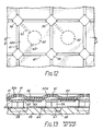
- a pyroelectric film 51 has an array of interconnected electrodes 52 formed on one side and an array of discrete electrodes 53 formed on the other side.
- Electrically conductive pads 54 are connected by long thin conductors 55 to the discrete electrodes 53 and by electrically conductive pillars 56 to input pads 57 of integrated circuitry 58 formed within adjacent regions of a silicon wafer 59, the circuit being effective to process electrical signals produced by the pyroelectric sensor elements.
- the input pads 57 are, as before separated by regions 60 of an electrically insulating layer.
- the interconnected electrodes 52 each carry extensions 52a in the form of an outer rim spaced from the pyroelectric film 51. There is a small gap 61 between the rims of adjacent interconnected electrodes except above the pillars 56 where the electrodes interconnect.
- the interconnected electrodes 52 and their extensions 52a carry a layer 63 of an infra-red absorbing material such as black gold or platinum black.
- the second device in accordance with the invention thus performs in an analogous manner to that described in relation to Figures 6 and 7 in that the rim shaped extensions 52a of the electrodes 52 with their overlying infra-red absorbant layer 63 intercept radiation in the areas corresponding to the unelectroded regions between the pillars 56 and discrete electrodes 53.
- the second device in accordance with the invention may be fabricated in a similar manner to that of the first device.
- One particular method of fabrication would be to use aluminium moulds in a general window frame configuration corresponding to the shape of the extensions 52a, in equivalent manner to the aluminium disc shaped moulds 45 shown in Figures 8 to 10.
Abstract
Description
- This invention relates to thermal imaging devices and in particular to thermal imaging devices comprising an array of pyroelectric detector elements responsive to infra-red radiation.
- The main factor limiting the performance of existing thermal imaging devices is the thermal conductance between adjacent detector elements and between each detector element and the supporting and interrogating structure.
- In our copending European Patent Application Nos. 89305494 and 89305496 there are described thermal imaging devices which are designed in such a way as to reduce the thermal conductance between the detector elements and the supporting and interrogating structure. These devices will now be described with reference to Figures 1 to 3 and 4 and 5 of the accompanying figures in which:
- Figure 1 shows a plan view of part of the electrode structure of the device described in European Patent Application No. 89305494;
- Figure 2 shows a plan view of part of a surface of the device shown in Figure 1, and
- Figure 3 shows a section along the line A-A′ of the device of Figures 1 and 2;
- Figure 4 shows a plan view of part of a surface of a device described in European Patent Application No. 89305496; and
- Figure 5 shows a section along the line B-B′ of the device of Figure 4.
- Referring to Figures 1 to 5 in which corresponding features are correspondingly labelled a pyroelectric film 1 has an array of
interconnected electrodes 2 formed on one side and an array ofdiscrete electrodes 3 formed on the other side. Electricallyconductive pads 4 are connected by longthin conductors 5 to thediscrete electrodes 3 and by electricallyconductive pillars 6 to input pads 7 of an integrated signal processing circuit located adjacent to the input pads of electrical circuits formed inregions 8 of a silicon wafer 9. The input pads 7 are separated byregions 10 of a passivating layer of an insulating material, for example silicon monoxide. In the arrangement of Figures 1 to 3 eachdiscrete electrode 3, as best seen in Figure 1, is square shaped with acentral gap 11 in which thepad 4 lies. The long,narrow conductor 5 extends around thepad 4 within thegap 11. Theinterconnected electrodes 2, as best seen in Figure 2 each have acentral hole 12 corresponding to thegap 11 in the respectivediscrete electrode 3 and may carry an infra-red absorption layer 13, consisting of, for example, black gold, platinum black or a metal-dielectric-metal sandwich structure. - Referring now to Figures 4 and 5, in the device illustrated in these figures the
discrete electrodes 3 are spaced from respective electricallyconductive pads 4 and connected to them by longnarrow conductors 5. The pillars are attached to respective electricallyconductive pads 4, each of which lies centrally disposed with respect to several (in the case illustrated four) adjacentdiscrete electrodes 3. The interconnectedelectrodes 2 are in positions corresponding to thediscrete electrodes 3 and again carry an appropriate infra-red absorption layer 13. - Both arrangements shown in Figures 1 to 5 provide a low, thermal conductance from the active areas of the
discrete electrodes 3 to thepillars 6 because the electrical connection between theelectrodes 3 andpillars 6 includes the longnarrow conductor 5. However, both arrangements involve significant areas either within (in the device illustrated in Figures 1-3) or around (in the device illustrated in Figures 4 and 5) thediscrete electrodes 3 where the incident radiation is wasted and consequently the signal to noise ratio of the device is reduced. In the device illustrated in Figures 4 and 5 thediscrete electrodes 3 could be brought closer together by meandering theconductor 5, as proposed inEuropean Patent Application No. 89305496 but there would still be significant incident radiation wasted at and around thepads 4. - It is an object of the present invention to provide a thermal imaging device of the type described in our copending European Patent Application Nos. 89305494 and 89305496 but wherein substantially the whole area of the pyroelectric film may be utilised to produce signals.
- According to the present invention a thermal imaging device comprises: a layer comprising pyroelectric material; an array of interconnected electrodes carried on one major surface of the layer; an array of discrete electrodes carried on the other major surface of the layer so as to define with the interconnected electrodes an array of pyroelectric detector elements; a plurality of pillars effective to support the layer, and to enable the passage of electrical signals between the detector element and an electrical signal processing means, each pillar being electrically connected to a discrete electrode by an elongate strip of electrically conductive material which extends over a region of the layer which carries no electrodes, the device being characterised in that said one major surface of the layer carries areas of infra-red absorbant material which extend into said regions carrying no electrodes, said areas being effective to conduct heat from each region to the adjacent pyroelectric detector element.
- The areas of infra-red absorbant material suitably comprise extensions of the interconnected electrodes arranged to overhang said regions out of electrical contact with the regions. In such an arrangement the interconnected electrodes and their extensions preferably carry infra-red absorbing layers.
- Two devices in accordance with the invention will now be described by way of example only with reference to the accompanying figures, of which:
- Figures 1 to 5 show the prior art arrangements already described;
- Figure 6 shows a plan view of part of a surface of a first device in accordance with the invention;
- Figure 7 is a section along the line C-C′ of the device shown in Figure 6;
- Figures 8-11 illustrate stages in the manufacture of part of the device shown in Figures 6 and 7;
- Figure 12 shows a plan view of part of a surface of a second device in accordance with the invention; and
- Figure 13 is a section along the line D-D′ of the device shown in Figure 12.
- Referring firstly to Figures 6 and 7, the device shown is a modification of the device shown in Figures 1-3 described herebefore. A
pyroelectric film 31 has an array ofinterconnected gold electrodes 32 formed on one side and an array ofdiscrete gold electrodes 33 on the other side. Electricallyconductive pads 34 are connected by long, thin, coiled conductors to thediscrete electrodes 33 and by electrically conductive pillars 36 to input pads 37 of integratedsignal processing circuits 38 formed within adjacent regions of asilicon wafer 39. The input pads 37 are separated by regions of apassivating layer 40 of an insulating material carried on thewafer 39. Thediscrete electrodes 33 are constructed in equivalent manner to those shown in Figure 1, described hereinbefore. Theinterconnected electrodes 32, differ from those shown in Figures 2 and 3 in that they haveextensions 32a which extend over regions of thepyroelectric film 31 carrying thecoiled conductors 35 on the other major surface. Theextension 32a are spaced from the surface of the pyroelectric film, such that the extensions resemble domes as can be seen in Figures 6 and 7. These domes have a centralsmall hole 41 to facilitate fabrication, as will be explained hereafter. The interconnectedelectrodes 32, together with theextensions 32a carry alayer 42 of an infra-red absorbing material, such as platinum black carried on aplatinum layer 43 or any other suitable infra-red absorber such as black gold or a metal-dielectric-metal sandwich structure. - It will be seen that the dome-
shaped extensions 32a with their overlying infra-red absorbing layers will intercept radiation in the regions around the pillars carrying theconductors 35, which would otherwise be wasted. By spacing theseextensions 32a away from thepyroelectric film 31 the thermal leakage from the absorber to the non-active i.e. non-electroded areas of the pyroelectric material is minimised. - It will be seen in the arrangement shown in Figures 6 and 7 that radiation passing through the
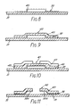
hole 41 in theelectrode extensions 32a will fall on an unelectroded part of the pyroelectric film. This may be disadvantageous, particularly in an array of very small pyroelectric sensor pixels, as it would result in an appreciable reduction in signal. This problem can be remedied by displacing theholes 41 laterally in theextensions 32a and arranging that theholes 41 overlie an electroded part of the pyroelectric layer. - Turning now to Figures 8-11 the
interconnected electrodes 32 may be constructed using the following procedure. - 1. Referring firstly to Figure 8 a layer of aluminium (e.g. 3 microns thick) is evaporated onto the top surface of the
pyroelectric film 31 and patterned so as to cover those areas of the film where the interconnected electrodes are extended byinner domes 32a which are spaced apart from the film. Thus an array of aluminium "mould"shapes 45 is formed. - 2. A thin gold interconnected electrode Pattern 32 (e.g. O.O3 microns thick) is then evaporated onto the top surface of the
pyroelectric layer 31 and thealuminium moulds 45. - 3. A
layer 43 of platinum (e.g. 0.1 micron thick) is evaporated onto the gold layer, and then converted partially or totally into a "platinum black" infra-redradiation absorbing surface 42 by standard procedures to produce the structure shown in Figure 9. - 4. A
polymer photoresist layer 47 is then deposited over the platinumblack surface 42. - 5. A pattern of
holes 41 over the central regions of thealuminium discs 45 is produced in thephotoresist layer 47 by standard photolithography techniques to provide access to thealuminium moulds 45 as shown in Figure 10. - 6. The
aluminium discs 45 are exposed by plasma etching through the platinum black 42,platinum 43, andgold 32 layers. Plasma etching is chosen as this technique gives fine resolution and straight side walls. - 7. The
aluminium discs 45 are removed by wet-etching in an acetic acid based solution or other appropriate etchant. - 8. Finally, the photoresist is removed, and the top electrode surface rinsed and dried to give the structure shown in Figure 11.
- It will be appreciated that there are many other ways of fabricating the device described including the use of alternative materials. In particular if the gold interconnected
electrodes 32 are formed sufficiently thick to possess a low sheet resistance for example less than 10 ohms per square, a thin layer of dielectric material, such as polyimide may be formed on the gold layer. A thin metallic overlayer, having an appropriate sheet resistance, for example 377 ohms per square, may then be deposited on the polyimide layer to form a metal-dielectric-metal infra-red radiation absorbing structure to take the place of the platinum/platinum black combination described herebefore. - Turning now to Figures 12 and 13, the second device in accordance with the invention is an adaptation of that shown in Figures 4 and 5, described hereinbefore. A
pyroelectric film 51 has an array ofinterconnected electrodes 52 formed on one side and an array ofdiscrete electrodes 53 formed on the other side. - Electrically
conductive pads 54 are connected by longthin conductors 55 to thediscrete electrodes 53 and by electricallyconductive pillars 56 to inputpads 57 ofintegrated circuitry 58 formed within adjacent regions of asilicon wafer 59, the circuit being effective to process electrical signals produced by the pyroelectric sensor elements. Theinput pads 57 are, as before separated byregions 60 of an electrically insulating layer. - The
interconnected electrodes 52 each carryextensions 52a in the form of an outer rim spaced from thepyroelectric film 51. There is asmall gap 61 between the rims of adjacent interconnected electrodes except above thepillars 56 where the electrodes interconnect. Theinterconnected electrodes 52 and theirextensions 52a carry alayer 63 of an infra-red absorbing material such as black gold or platinum black. The second device in accordance with the invention thus performs in an analogous manner to that described in relation to Figures 6 and 7 in that the rim shapedextensions 52a of theelectrodes 52 with their overlying infra-redabsorbant layer 63 intercept radiation in the areas corresponding to the unelectroded regions between thepillars 56 anddiscrete electrodes 53. - It will be appreciated that the second device in accordance with the invention may be fabricated in a similar manner to that of the first device. One particular method of fabrication would be to use aluminium moulds in a general window frame configuration corresponding to the shape of the
extensions 52a, in equivalent manner to the aluminium disc shapedmoulds 45 shown in Figures 8 to 10.
Claims (8)
Priority Applications (1)
| Application Number | Priority Date | Filing Date | Title |
|---|---|---|---|
| AT89312730T ATE93962T1 (en) | 1988-12-20 | 1989-12-06 | DEVICE FOR THERMAL IMAGING. |
Applications Claiming Priority (2)
| Application Number | Priority Date | Filing Date | Title |
|---|---|---|---|
| GB888829685A GB8829685D0 (en) | 1988-12-20 | 1988-12-20 | Thermal imaging device |
| GB8829685 | 1988-12-20 |
Publications (3)
| Publication Number | Publication Date |
|---|---|
| EP0375205A2 true EP0375205A2 (en) | 1990-06-27 |
| EP0375205A3 EP0375205A3 (en) | 1991-08-21 |
| EP0375205B1 EP0375205B1 (en) | 1993-09-01 |
Family
ID=10648800
Family Applications (1)
| Application Number | Title | Priority Date | Filing Date |
|---|---|---|---|
| EP89312730A Expired - Lifetime EP0375205B1 (en) | 1988-12-20 | 1989-12-06 | Thermal imaging device |
Country Status (7)
| Country | Link |
|---|---|
| US (1) | US5077474A (en) |
| EP (1) | EP0375205B1 (en) |
| JP (1) | JPH02215583A (en) |
| AT (1) | ATE93962T1 (en) |
| CA (1) | CA2005771A1 (en) |
| DE (1) | DE68908863T2 (en) |
| GB (1) | GB8829685D0 (en) |
Cited By (5)
| Publication number | Priority date | Publication date | Assignee | Title |
|---|---|---|---|---|
| EP0454398A2 (en) * | 1990-04-24 | 1991-10-30 | THORN EMI plc | Thermal detector device |
| GB2321780A (en) * | 1997-01-31 | 1998-08-05 | Mitsubishi Electric Corp | Sensor element and manufacturting element |
| EP0859413A2 (en) * | 1997-01-27 | 1998-08-19 | Mitsubishi Denki Kabushiki Kaisha | Infrared focal plane array |
| FR2776422A1 (en) * | 1998-03-04 | 1999-09-24 | Marconi Electronic Syst Ltd | ELECTROMAGNETIC RADIATION DETECTOR, ESPECIALLY THERMAL |
| US6239433B1 (en) * | 1997-01-14 | 2001-05-29 | Infrared Integrated Systems. Ltd. | Sensors using detector arrays |
Families Citing this family (6)
| Publication number | Priority date | Publication date | Assignee | Title |
|---|---|---|---|---|
| US5288649A (en) * | 1991-09-30 | 1994-02-22 | Texas Instruments Incorporated | Method for forming uncooled infrared detector |
| JPH0743215A (en) * | 1993-05-24 | 1995-02-14 | Mitsubishi Electric Corp | Infrared detecting element |
| US5485010A (en) * | 1994-01-13 | 1996-01-16 | Texas Instruments Incorporated | Thermal isolation structure for hybrid thermal imaging system |
| US5653892A (en) * | 1994-04-04 | 1997-08-05 | Texas Instruments Incorporated | Etching of ceramic materials with an elevated thin film |
| US5602392A (en) * | 1995-01-31 | 1997-02-11 | Texas Instruments | Thermal crosstalk reduction for infrared detectors with common electrodes |
| GB9710843D0 (en) * | 1997-05-28 | 1997-07-23 | Secr Defence | A thermal detector array |
Citations (3)
| Publication number | Priority date | Publication date | Assignee | Title |
|---|---|---|---|---|
| US4532424A (en) * | 1983-04-25 | 1985-07-30 | Rockwell International Corporation | Pyroelectric thermal detector array |
| JPS6166129A (en) * | 1984-09-07 | 1986-04-04 | Murata Mfg Co Ltd | Pyroelectric type infrared-ray sensor array |
| EP0298568A2 (en) * | 1987-07-10 | 1989-01-11 | Gec-Marconi Limited | Arrays of infrared detector elements |
Family Cites Families (3)
| Publication number | Priority date | Publication date | Assignee | Title |
|---|---|---|---|---|
| US4722612A (en) * | 1985-09-04 | 1988-02-02 | Wahl Instruments, Inc. | Infrared thermometers for minimizing errors associated with ambient temperature transients |
| GB2200245B (en) * | 1985-09-12 | 1989-09-13 | Plessey Co Plc | Thermal detector |
| GB8812955D0 (en) * | 1988-06-01 | 1988-10-05 | Emi Plc Thorn | Thermal imaging |
-
1988
- 1988-12-20 GB GB888829685A patent/GB8829685D0/en active Pending
-
1989
- 1989-12-06 DE DE89312730T patent/DE68908863T2/en not_active Expired - Fee Related
- 1989-12-06 AT AT89312730T patent/ATE93962T1/en not_active IP Right Cessation
- 1989-12-06 EP EP89312730A patent/EP0375205B1/en not_active Expired - Lifetime
- 1989-12-08 US US07/447,135 patent/US5077474A/en not_active Expired - Fee Related
- 1989-12-18 CA CA002005771A patent/CA2005771A1/en not_active Abandoned
- 1989-12-19 JP JP1327458A patent/JPH02215583A/en active Pending
Patent Citations (3)
| Publication number | Priority date | Publication date | Assignee | Title |
|---|---|---|---|---|
| US4532424A (en) * | 1983-04-25 | 1985-07-30 | Rockwell International Corporation | Pyroelectric thermal detector array |
| JPS6166129A (en) * | 1984-09-07 | 1986-04-04 | Murata Mfg Co Ltd | Pyroelectric type infrared-ray sensor array |
| EP0298568A2 (en) * | 1987-07-10 | 1989-01-11 | Gec-Marconi Limited | Arrays of infrared detector elements |
Non-Patent Citations (1)
| Title |
|---|
| PATENT ABSTRACTS OF JAPAN vol. 10, no. 232 (P-486)(2288) August 12, 1986 & JP-A-61 066 129 (MURATA ) April 4, 1986 * |
Cited By (12)
| Publication number | Priority date | Publication date | Assignee | Title |
|---|---|---|---|---|
| EP0454398A2 (en) * | 1990-04-24 | 1991-10-30 | THORN EMI plc | Thermal detector device |
| EP0454398A3 (en) * | 1990-04-24 | 1992-03-25 | Thorn Emi Plc | Thermal detector device |
| US5193911A (en) * | 1990-04-24 | 1993-03-16 | Thorn Emi Plc | Thermal detector device |
| US6239433B1 (en) * | 1997-01-14 | 2001-05-29 | Infrared Integrated Systems. Ltd. | Sensors using detector arrays |
| EP0859413A2 (en) * | 1997-01-27 | 1998-08-19 | Mitsubishi Denki Kabushiki Kaisha | Infrared focal plane array |
| EP0859413A3 (en) * | 1997-01-27 | 1999-01-20 | Mitsubishi Denki Kabushiki Kaisha | Infrared focal plane array |
| US6031231A (en) * | 1997-01-27 | 2000-02-29 | Mitsubishi Denki Kabushiki Kaisha | Infrared focal plane array |
| EP1837911A3 (en) * | 1997-01-27 | 2011-05-04 | Mitsubishi Denki Kabushiki Kaisha | Infrared focal plane array |
| GB2321780A (en) * | 1997-01-31 | 1998-08-05 | Mitsubishi Electric Corp | Sensor element and manufacturting element |
| GB2321780B (en) * | 1997-01-31 | 1999-05-12 | Mitsubishi Electric Corp | Sensor element and manufacturing method thereof |
| US5998816A (en) * | 1997-01-31 | 1999-12-07 | Mitsubishi Denki Kabushiki Kaisha | Sensor element with removal resistance region |
| FR2776422A1 (en) * | 1998-03-04 | 1999-09-24 | Marconi Electronic Syst Ltd | ELECTROMAGNETIC RADIATION DETECTOR, ESPECIALLY THERMAL |
Also Published As
| Publication number | Publication date |
|---|---|
| ATE93962T1 (en) | 1993-09-15 |
| CA2005771A1 (en) | 1990-06-20 |
| EP0375205A3 (en) | 1991-08-21 |
| DE68908863T2 (en) | 1994-03-24 |
| DE68908863D1 (en) | 1993-10-07 |
| GB8829685D0 (en) | 1989-02-15 |
| JPH02215583A (en) | 1990-08-28 |
| EP0375205B1 (en) | 1993-09-01 |
| US5077474A (en) | 1991-12-31 |
Similar Documents
| Publication | Publication Date | Title |
|---|---|---|
| US7405403B2 (en) | Bolometric detector, device for detecting infrared radiation using such a detector and method for producing this detector | |
| JP4137196B2 (en) | Infrared detector and manufacturing method thereof | |
| US5688699A (en) | Microbolometer | |
| US4663529A (en) | Thermal imaging device and a method of manufacturing a thermal imaging device | |
| KR100704948B1 (en) | Thermal sensor and method of making same | |
| EP0375205B1 (en) | Thermal imaging device | |
| US6094127A (en) | Infrared bolometer and method for manufacturing same | |
| US5939971A (en) | Infrared bolometer | |
| JP2002286673A (en) | Gas sensor and its manufacturing method | |
| US7105819B2 (en) | Infrared ray sensor using silicon oxide film as infrared ray absorption layer and method of fabricating the same | |
| EP0345047B1 (en) | Thermal imaging device | |
| US7232998B2 (en) | Bolometer-type infrared solid-state image sensor | |
| DE4221037C2 (en) | Thermal radiation sensor | |
| JPH11148861A (en) | Microbidge structure | |
| US5420420A (en) | Infrared detector | |
| US20030201395A1 (en) | Thermal radiation detection device with a limited number of anchor points | |
| US4847500A (en) | Thermal detector | |
| EP1137918A1 (en) | Infrared bolometer | |
| JPH11108760A (en) | Thermal type infrared detecting delement and its manufacture | |
| EP0345049B1 (en) | Thermal imaging device | |
| US4942301A (en) | Thermal imaging device | |
| EP1141669B1 (en) | Infrared bolometer and method for manufacturing same | |
| JPH04342177A (en) | Thermopile | |
| JPH02201229A (en) | Infrared sensor | |
| JPS60167388A (en) | Photodetector |
Legal Events
| Date | Code | Title | Description |
|---|---|---|---|
| PUAI | Public reference made under article 153(3) epc to a published international application that has entered the european phase |
Free format text: ORIGINAL CODE: 0009012 |
|
| AK | Designated contracting states |
Kind code of ref document: A2 Designated state(s): AT BE CH DE ES FR GB GR IT LI LU NL SE |
|
| PUAL | Search report despatched |
Free format text: ORIGINAL CODE: 0009013 |
|
| AK | Designated contracting states |
Kind code of ref document: A3 Designated state(s): AT BE CH DE ES FR GB GR IT LI LU NL SE |
|
| 17P | Request for examination filed |
Effective date: 19920210 |
|
| 17Q | First examination report despatched |
Effective date: 19930217 |
|
| GRAA | (expected) grant |
Free format text: ORIGINAL CODE: 0009210 |
|
| AK | Designated contracting states |
Kind code of ref document: B1 Designated state(s): AT BE CH DE ES FR GB GR IT LI LU NL SE |
|
| PG25 | Lapsed in a contracting state [announced via postgrant information from national office to epo] |
Ref country code: SE Effective date: 19930901 Ref country code: GR Free format text: LAPSE BECAUSE OF FAILURE TO SUBMIT A TRANSLATION OF THE DESCRIPTION OR TO PAY THE FEE WITHIN THE PRESCRIBED TIME-LIMIT Effective date: 19930901 Ref country code: ES Free format text: THE PATENT HAS BEEN ANNULLED BY A DECISION OF A NATIONAL AUTHORITY Effective date: 19930901 Ref country code: BE Effective date: 19930901 Ref country code: AT Effective date: 19930901 |
|
| REF | Corresponds to: |
Ref document number: 93962 Country of ref document: AT Date of ref document: 19930915 Kind code of ref document: T |
|
| REF | Corresponds to: |
Ref document number: 68908863 Country of ref document: DE Date of ref document: 19931007 |
|
| ET | Fr: translation filed | ||
| ITF | It: translation for a ep patent filed |
Owner name: FUMERO BREVETTI S.N.C. |
|
| PG25 | Lapsed in a contracting state [announced via postgrant information from national office to epo] |
Ref country code: LU Free format text: LAPSE BECAUSE OF NON-PAYMENT OF DUE FEES Effective date: 19931231 |
|
| PLBE | No opposition filed within time limit |
Free format text: ORIGINAL CODE: 0009261 |
|
| STAA | Information on the status of an ep patent application or granted ep patent |
Free format text: STATUS: NO OPPOSITION FILED WITHIN TIME LIMIT |
|
| 26N | No opposition filed | ||
| REG | Reference to a national code |
Ref country code: CH Ref legal event code: PUE Owner name: THORN EMI PLC TRANSFER- CENTRAL RESEARCH LABORATOR |
|
| NLS | Nl: assignments of ep-patents |
Owner name: CENTRAL RESEARCH LABORATORIES LIMITED |
|
| PGFP | Annual fee paid to national office [announced via postgrant information from national office to epo] |
Ref country code: FR Payment date: 19960924 Year of fee payment: 8 |
|
| PGFP | Annual fee paid to national office [announced via postgrant information from national office to epo] |
Ref country code: GB Payment date: 19960925 Year of fee payment: 8 |
|
| REG | Reference to a national code |
Ref country code: FR Ref legal event code: TP Free format text: CORRECTION |
|
| PGFP | Annual fee paid to national office [announced via postgrant information from national office to epo] |
Ref country code: CH Payment date: 19961202 Year of fee payment: 8 |
|
| REG | Reference to a national code |
Ref country code: GB Ref legal event code: 732E |
|
| PGFP | Annual fee paid to national office [announced via postgrant information from national office to epo] |
Ref country code: NL Payment date: 19961231 Year of fee payment: 8 |
|
| PGFP | Annual fee paid to national office [announced via postgrant information from national office to epo] |
Ref country code: DE Payment date: 19970224 Year of fee payment: 8 |
|
| PG25 | Lapsed in a contracting state [announced via postgrant information from national office to epo] |
Ref country code: GB Free format text: LAPSE BECAUSE OF NON-PAYMENT OF DUE FEES Effective date: 19971206 |
|
| PG25 | Lapsed in a contracting state [announced via postgrant information from national office to epo] |
Ref country code: LI Free format text: LAPSE BECAUSE OF NON-PAYMENT OF DUE FEES Effective date: 19971231 Ref country code: FR Free format text: THE PATENT HAS BEEN ANNULLED BY A DECISION OF A NATIONAL AUTHORITY Effective date: 19971231 Ref country code: CH Free format text: LAPSE BECAUSE OF NON-PAYMENT OF DUE FEES Effective date: 19971231 |
|
| PG25 | Lapsed in a contracting state [announced via postgrant information from national office to epo] |
Ref country code: NL Free format text: LAPSE BECAUSE OF NON-PAYMENT OF DUE FEES Effective date: 19980701 |
|
| GBPC | Gb: european patent ceased through non-payment of renewal fee |
Effective date: 19971206 |
|
| REG | Reference to a national code |
Ref country code: CH Ref legal event code: PL |
|
| NLV4 | Nl: lapsed or anulled due to non-payment of the annual fee |
Effective date: 19980701 |
|
| PG25 | Lapsed in a contracting state [announced via postgrant information from national office to epo] |
Ref country code: DE Free format text: LAPSE BECAUSE OF NON-PAYMENT OF DUE FEES Effective date: 19980901 |
|
| REG | Reference to a national code |
Ref country code: FR Ref legal event code: ST |
|
| PG25 | Lapsed in a contracting state [announced via postgrant information from national office to epo] |
Ref country code: IT Free format text: LAPSE BECAUSE OF NON-PAYMENT OF DUE FEES;WARNING: LAPSES OF ITALIAN PATENTS WITH EFFECTIVE DATE BEFORE 2007 MAY HAVE OCCURRED AT ANY TIME BEFORE 2007. THE CORRECT EFFECTIVE DATE MAY BE DIFFERENT FROM THE ONE RECORDED. Effective date: 20051206 |