EP0345047B1 - Thermal imaging device - Google Patents
Thermal imaging device Download PDFInfo
- Publication number
- EP0345047B1 EP0345047B1 EP89305494A EP89305494A EP0345047B1 EP 0345047 B1 EP0345047 B1 EP 0345047B1 EP 89305494 A EP89305494 A EP 89305494A EP 89305494 A EP89305494 A EP 89305494A EP 0345047 B1 EP0345047 B1 EP 0345047B1
- Authority
- EP
- European Patent Office
- Prior art keywords
- layer
- discrete
- pyroelectric
- array
- inter
- Prior art date
- Legal status (The legal status is an assumption and is not a legal conclusion. Google has not performed a legal analysis and makes no representation as to the accuracy of the status listed.)
- Expired - Lifetime
Links
Images

Classifications
-
- H—ELECTRICITY
- H10—SEMICONDUCTOR DEVICES; ELECTRIC SOLID-STATE DEVICES NOT OTHERWISE PROVIDED FOR
- H10N—ELECTRIC SOLID-STATE DEVICES NOT OTHERWISE PROVIDED FOR
- H10N15/00—Thermoelectric devices without a junction of dissimilar materials; Thermomagnetic devices, e.g. using the Nernst-Ettingshausen effect
- H10N15/10—Thermoelectric devices using thermal change of the dielectric constant, e.g. working above and below the Curie point
-
- G—PHYSICS
- G01—MEASURING; TESTING
- G01J—MEASUREMENT OF INTENSITY, VELOCITY, SPECTRAL CONTENT, POLARISATION, PHASE OR PULSE CHARACTERISTICS OF INFRARED, VISIBLE OR ULTRAVIOLET LIGHT; COLORIMETRY; RADIATION PYROMETRY
- G01J5/00—Radiation pyrometry, e.g. infrared or optical thermometry
- G01J5/10—Radiation pyrometry, e.g. infrared or optical thermometry using electric radiation detectors
- G01J5/34—Radiation pyrometry, e.g. infrared or optical thermometry using electric radiation detectors using capacitors, e.g. pyroelectric capacitors
-
- H—ELECTRICITY
- H10—SEMICONDUCTOR DEVICES; ELECTRIC SOLID-STATE DEVICES NOT OTHERWISE PROVIDED FOR
- H10N—ELECTRIC SOLID-STATE DEVICES NOT OTHERWISE PROVIDED FOR
- H10N19/00—Integrated devices, or assemblies of multiple devices, comprising at least one thermoelectric or thermomagnetic element covered by groups H10N10/00 - H10N15/00
-
- G—PHYSICS
- G01—MEASURING; TESTING
- G01J—MEASUREMENT OF INTENSITY, VELOCITY, SPECTRAL CONTENT, POLARISATION, PHASE OR PULSE CHARACTERISTICS OF INFRARED, VISIBLE OR ULTRAVIOLET LIGHT; COLORIMETRY; RADIATION PYROMETRY
- G01J5/00—Radiation pyrometry, e.g. infrared or optical thermometry
- G01J5/10—Radiation pyrometry, e.g. infrared or optical thermometry using electric radiation detectors
- G01J5/34—Radiation pyrometry, e.g. infrared or optical thermometry using electric radiation detectors using capacitors, e.g. pyroelectric capacitors
- G01J2005/345—Arrays
Definitions
- This invention relates to thermal imaging devices and in particular to thermal imaging devices comprising an array of pyroelectric detector elements responsive to infrared radiation.
- the main factor limiting the performance of existing pyroelectric imagers is the thermal conductance between adjacent detector elements and between each detector element and the supporting and interrogating structure.
- U.K. Patent Application No. GB-A-2163596 discloses a thermal imaging device comprising a ferroelectric slab bearing a common electrode on one main surface and a signal electrode structure on the opposite main surface.
- the signal electrode structure is electrically connected to electrodes of a circuit substrate by means of conductors.
- the transverse heat conduction between adjacent conductors is reduced by incorporating each conductor on a bore in a respective pillar of thermally insulating material, the pillars also being effective to support the ferroelectric slab.
- a thermal imaging device comprises: a layer comprising pyroelectric material; an array of inter-connected electrodes carried on one major surface of the layer; an array of discrete electrodes carried on the other major surface of the layer; a plurality of pillars effective to support the layer and to enable the passage of electrical signals between the discrete electrodes and an electrical signal processing means, each pillar being located on an electrical contact region within a nonelectroded region of said other major surface within a respective discrete electrode, the contact region and discrete electrode being electrically connected by a respective elongate region of electrically conductive material extending over said nonelectroded region.
- the layer may comprise a continuous film of pyroelectric material, for example, a pyroelectric polymer.
- the layer may comprise an array of discrete regions of pyroelectric material carried on a continuous film of dielectric material.
- suitable pyroelectric materials are lead lanthanum zirconium titanate, lead zirconium titanate, lead titanate and barium titanate.
- the pyroelectric material suitably comprises polyvinylidene fluoride (PVDF) or a copolymer of vinylidene fluoride with, for example, trifluoroethylene (P(VDF-TrFE)).
- PVDF polyvinylidene fluoride
- P(VDF-TrFE) polyvinylidene fluoride with, for example, trifluoroethylene
- the pyroelectric material in the device may comprise material which is inherently pyroelectric, or material whose pyroelectric characteristics are induced (e.g. by appropriate poling of ferroelectric material).
- the elongate region suitably has a length to width ratio of at least 5.
- said array of inter-connected electrodes comprises an array of electrically conductive regions carried on said one surface at positions corresponding to the positions of the discrete electrodes on the other surface, said electrically conductive regions being inter-connected by electrical conductors which are narrow compared with the width of the electrically conductive regions.
- a process of making a thermal imaging device comprises: forming a layer comprising pyroelectric material; forming an array of discrete electrodes on one major surface of the layer, each discrete electrode substantially surrounding a nonelectroded portion of the one surface; forming electrically conductive contact regions within the nonelectroded regions together with an elongate region of electrically conductive material extending over the nonelectroded region and electrically connecting each discrete electrode to a respective contact region; forming respective electrically conductive support pillars on each contact region; connecting the support pillars to the input terminals of a signal processing means; and forming an inter-connected electrode structure on the other major surface of the layer, at positions aligned with the array of discrete electrodes.
- the step of forming a layer suitably comprises: spin-coating a layer of a polymer on an electrically conductive substrate; treating the polymer such that it is made pyroelectric; and dissolving away the substrate before forming the inter-connected electrode structure on the other major surface of the layer.
- the inter-connected electrode structure is formed on one surface of the dielectric material; and the step of forming a layer comprises: forming an array of regions of pyroelectric material on the inter-connected electrodes and exposed regions of the one surface of the dielectric film.
- the optimum thickness of pyroelectric materials in hybrid structures of low thermal conductance is of the order of one ⁇ m.
- the thermal conductance of metal electrodes dominates that of a pyroelectric material one ⁇ m thick even if the metal film is only 0.03 ⁇ m, the thickness below which gold films become discontinuous.
- the use of a long, narrow electrical conductor to connect each pillar and discrete electrode ensures that the thermal conductance from the respective pixel to the support pillar is small.
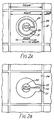
- a pyroelectric film 21 of, for example, P(VDF-TrFE) has a pattern of inter-connected electrodes 22 formed on one side and an array of discrete electrodes 24 on the other side. Electrically conductive pads 23 are connected by a respective narrow electrically conducting strip 25 which passes almost completely round the pad 23 to the surrounding discrete electrodes 24. Pillars 26 are attached at one end to pads and at the other end to input pads 27 of an integrated circuit 28 formed on the substrate 29. Thus thermal insulation is provided by the gap 31 between each pad 23 and surrounding discrete electrode 24 . A gap 32 separates adjacent pixels.
- Figure 2(b) shows an alternative arrangement of the structure carried on the second side of the film 21. This again comprises a pad 23, a gap 31 around the pad and a discrete electrode 24. The electrode 24 is however linked to the pad 23 by a narrow electrically conductive linear strip 33 which extends almost to the edge of the discrete electrode 24.
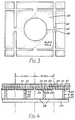
- FIG 3 shows a plan view of the inter-connected electrodes shown at 22 in Figure 1.
- the inter-connected electrodes each have a central hole 30 in the area corresponding to the pads 23 and to the gap 31 within the discrete electrodes 24 shown in Figures 2(a) or 2(b).
- the central hole 30 ensures that the inter-connected electrodes do not increase the thermal conductance between the pads 23 and discrete electrodes 24.
- the thermal conductance from pixel to pixel is kept low by the use of a thin pyroelectric film and by the gap 41 between adjacent pixel areas of the inter-connected electrodes, electrical continuity being provided by narrow conducting strips 42 across the gaps 41.
- the inter-connected electrodes will generally be covered by an infra-red absorbent layer 43, for example a layer of black gold, platinum black, or a metal-dielectric-metal sandwich structure.
- an infra-red absorbent layer 43 for example a layer of black gold, platinum black, or a metal-dielectric-metal sandwich structure.
- the discrete electrode-pyroelectric film-interconnected electrode layers together comprise a 1/4 wavelength thickness for infra-red radiation (i.e. about 1.5 ⁇ m) this structure itself will constitute an efficient thermal absorber.
- a dielectric film 51 has a pattern of inter-connected electrodes 22 formed on a surface.
- An array of discrete pyroelectric regions 52 is formed on the electrodes 22 and the dielectric film 51 where exposed and an array of discrete electrodes formed on the pyroelectric elements.
- the inter-connected electrodes 22 and the discrete electrodes 24 surrounding a central conductive pad and conducting strips 25 are similar to those described hereinbefore with reference to Figures 3 and 2 respectively.
- the arrangement of the pillars 26, integrated circuits 28, substrate 29 and infra-red absorbant layer 43 is similar to that described hereinbefore with reference to Figure 1.
- the pyroelectric regions may be again formed, for example, from a pyroelectric polymer, or may, for example, be formed from a ferroelectric ceramic material.
- the pyroelectric film 21 is a copolymer of polyvinylidene fluoride (PVDF), but any thin self-supporting pyroelectric material could be employed.
- PVDF polyvinylidene fluoride
- an optically flat electrically conductive substrate is spin-coated with polyvinylidene fluoride-trifluoroethylene copolymer (VDF-TrFE).
- the substrate might be a silicon wafer, or any material which can be etched or dissolved away in a subsequent process.
- the VDF-TrFE copolymer may be dissolved in a mixture of acetone and dimethyl formamide, or in one or more of several possible solvents for VDF copolymers.
- the spin-coated polymer layer is chosen to be an optimum thickness for the infra-red detection application, and will be typically 1 ⁇ m thick.
- the polymer membrane is made pyroelectric by any standard technique such as by corona poling.
- a gold pattern of discrete electrodes 24, pads 23 and strips 25 such as those shown in Figure 2a is then formed on the pyroelectric film 21 by standard photolithographic techniques. This will be referred to as the bottom electrode.
- the pattern repeat distance is typically 100 ⁇ m and the gold thickness O.O3 ⁇ m.
- Each element of the pattern will be referred to as a pixel, with a typical array having at least 100 x 100 pixels.
- the strips 25 will typically be 3 ⁇ m wide.
- the gap region 31 of the electrode (60 ⁇ m in external diameter) around the centre region provides the thermal isolation between the centre region 23 and the active thermal detection region 24 of each pixel.
- Gold support pillars - typically 25 ⁇ m diameter and 25 ⁇ m high - are grown by standard photolithographic and electroplating techniques on the input pads 27 of an integrated circuit 28.
- Figures 1 and 2a show the position where the pillars connect to the discrete electrode pattern.
- the whole device is then inverted on to a complementary electronic measurement circuit on a silicon chip 29, and electrical connection made to the gold pillars, for example by soft solder.
- the original substrate material is etched or dissolved to leave the polymer layer supported by the gold pillars.
- the inter-connected electrodes are formed by standard photolithographic techniques on the exposed side of the pyroelectric film 21.
- the inter-connected electrode pattern registers with the discrete electrodes so that the central regions of pyroelectric film 21 are left unelectroded. These regions provide the thermal isolation between the pillars and the active, electroded, outer region of each pixel.
- An additional infra-red absorbing layer may also be deposited in the same pattern and position as the inter-connected electrode structure.
- the thermal mass of the inter-connected electrodes and absorbing layer will, in general, be greater than that of the discrete electrodes but this extra material will not increase the conductance between detector and silicon chip.
- a pattern of inter-connected electrodes is formed by standard photolithographic techniques on a thin film of a dielectric (for example polyimide, silicon oxide, silicon nitride or silicon oxy-nitride).
- a dielectric for example polyimide, silicon oxide, silicon nitride or silicon oxy-nitride.
- This inter-connected electrode pattern is of the form illustrated in Figure 3 and carries an infra-red absorbing material, such as black gold.
- the inter-connected electrode pattern is spin-coated with polyvinylidene fluoride-trifluoroethylene copolymer (P(VDF-TrFE)), which might be dissolved in a mixture of acetone and dimethyl formamide, or in one or more of several possible solvents for VDF copolymers.
- P(VDF-TrFE) polyvinylidene fluoride-trifluoroethylene copolymer
- the spin-coated polymer layer is chosen to be an optimum thickness for the infrared detection application, and will be typically 1 ⁇ m thick and is formed as an array of discrete elements of the copolymer as shown in Figure 4.
- the polymer membrane or elements are made pyroelectric by any standard technique such as by corona poling.
- a gold pattern of discrete electrodes, pads, and inter-connecting strip such as the one shown in Figure 2a is then formed on the pyroelectric elements by standard photolithographic techniques.
- the pattern repeat distance is typically 100 ⁇ m and the gold thickness O.O3 ⁇ m.
- Each element of the pattern will be referred to as a pixel, and a typical array has at least 100 x 100 pixels.
- the gap region 31 of the electrode (60 ⁇ m in external diameter) around the centre region provides the thermal isolation between the centre region 23 and the active thermal detection region 24 of each pixel.
- Gold support pillars - typically 25 ⁇ m diameter and 25 ⁇ m high - are grown by standard photolithographic and electroplating techniques on the input pads of an integrated circuit.
- the whole device is then inverted on to the complementary electronic measurement circuit on a silicon chip 29, and electrical connection made to the gold pillars, for example by soft solder.
Landscapes
- Engineering & Computer Science (AREA)
- Power Engineering (AREA)
- Physics & Mathematics (AREA)
- General Physics & Mathematics (AREA)
- Spectroscopy & Molecular Physics (AREA)
- Transforming Light Signals Into Electric Signals (AREA)
- Photometry And Measurement Of Optical Pulse Characteristics (AREA)
- Radiation Pyrometers (AREA)
- Color Television Image Signal Generators (AREA)
- Carbon And Carbon Compounds (AREA)
- Light Receiving Elements (AREA)
Abstract
Description
- This invention relates to thermal imaging devices and in particular to thermal imaging devices comprising an array of pyroelectric detector elements responsive to infrared radiation.
- The main factor limiting the performance of existing pyroelectric imagers is the thermal conductance between adjacent detector elements and between each detector element and the supporting and interrogating structure.
- U.K. Patent Application No. GB-A-2163596 discloses a thermal imaging device comprising a ferroelectric slab bearing a common electrode on one main surface and a signal electrode structure on the opposite main surface. The signal electrode structure is electrically connected to electrodes of a circuit substrate by means of conductors. The transverse heat conduction between adjacent conductors is reduced by incorporating each conductor on a bore in a respective pillar of thermally insulating material, the pillars also being effective to support the ferroelectric slab.
- Contact regions connected to the discrete electrodes of pyroelectric detector elements by elongate strips are disclosed in JP-A-61 66129.
- It is an object of the present invention to provide an alternative thermal imaging device in which the pyroelectric detector elements are supported by pillars, but wherein the thermal losses between the detector elements and supporting pillars are reduced.
- According to a first aspect of the present invention a thermal imaging device comprises: a layer comprising pyroelectric material; an array of inter-connected electrodes carried on one major surface of the layer; an array of discrete electrodes carried on the other major surface of the layer; a plurality of pillars effective to support the layer and to enable the passage of electrical signals between the discrete electrodes and an electrical signal processing means, each pillar being located on an electrical contact region within a nonelectroded region of said other major surface within a respective discrete electrode, the contact region and discrete electrode being electrically connected by a respective elongate region of electrically conductive material extending over said nonelectroded region.
- The layer may comprise a continuous film of pyroelectric material, for example, a pyroelectric polymer.
- Alternatively the layer may comprise an array of discrete regions of pyroelectric material carried on a continuous film of dielectric material. Examples of suitable pyroelectric materials are lead lanthanum zirconium titanate, lead zirconium titanate, lead titanate and barium titanate.
- The pyroelectric material suitably comprises polyvinylidene fluoride (PVDF) or a copolymer of vinylidene fluoride with, for example, trifluoroethylene (P(VDF-TrFE)).
- The pyroelectric material in the device may comprise material which is inherently pyroelectric, or material whose pyroelectric characteristics are induced (e.g. by appropriate poling of ferroelectric material).
- The elongate region suitably has a length to width ratio of at least 5.
- In a preferred embodiment, said array of inter-connected electrodes comprises an array of electrically conductive regions carried on said one surface at positions corresponding to the positions of the discrete electrodes on the other surface, said electrically conductive regions being inter-connected by electrical conductors which are narrow compared with the width of the electrically conductive regions.
- According to a second aspect of the present invention a process of making a thermal imaging device comprises: forming a layer comprising pyroelectric material; forming an array of discrete electrodes on one major surface of the layer, each discrete electrode substantially surrounding a nonelectroded portion of the one surface; forming electrically conductive contact regions within the nonelectroded regions together with an elongate region of electrically conductive material extending over the nonelectroded region and electrically connecting each discrete electrode to a respective contact region; forming respective electrically conductive support pillars on each contact region; connecting the support pillars to the input terminals of a signal processing means; and forming an inter-connected electrode structure on the other major surface of the layer, at positions aligned with the array of discrete electrodes.
- Where the layer is a pyroelectric polymer, the step of forming a layer suitably comprises: spin-coating a layer of a polymer on an electrically conductive substrate; treating the polymer such that it is made pyroelectric; and dissolving away the substrate before forming the inter-connected electrode structure on the other major surface of the layer.
- Where the layer comprises an array of discrete regions of pyroelectric material carried on a continuous film of dielectric material, the inter-connected electrode structure is formed on one surface of the dielectric material; and the step of forming a layer comprises: forming an array of regions of pyroelectric material on the inter-connected electrodes and exposed regions of the one surface of the dielectric film.
- The optimum thickness of pyroelectric materials in hybrid structures of low thermal conductance is of the order of one µm. The thermal conductance of metal electrodes dominates that of a pyroelectric material one µm thick even if the metal film is only 0.03 µm, the thickness below which gold films become discontinuous. The use of a long, narrow electrical conductor to connect each pillar and discrete electrode ensures that the thermal conductance from the respective pixel to the support pillar is small.
- Two thermal imaging devices in accordance with the invention together with methods for fabricating the devices, will now be described, by way of example only, with reference to the accompanying drawings of which:
- Figure 1 shows a section of the first thermal imaging device;
- Figure 2(a) is a schematic sectional view of part of a surface of the device of Figure 1 illustrating the discrete electrodes;
- Figure 2(b) is a schematic sectional view corresponding to Figure 2(a) illustrating a modified arrangement;
- Figure 3 shows a plan view of the device illustrating the inter-connected electrode arrangement; and
- Figure 4 shows a section of the second thermal imaging device.
- Referring firstly to Figures 1 and 2(a), a
pyroelectric film 21 of, for example, P(VDF-TrFE) has a pattern ofinter-connected electrodes 22 formed on one side and an array ofdiscrete electrodes 24 on the other side. Electricallyconductive pads 23 are connected by a respective narrow electrically conductingstrip 25 which passes almost completely round thepad 23 to the surroundingdiscrete electrodes 24.Pillars 26 are attached at one end to pads and at the other end toinput pads 27 of an integratedcircuit 28 formed on thesubstrate 29. Thus thermal insulation is provided by thegap 31 between eachpad 23 and surroundingdiscrete electrode 24 . Agap 32 separates adjacent pixels. Figure 2(b) shows an alternative arrangement of the structure carried on the second side of thefilm 21. This again comprises apad 23, agap 31 around the pad and adiscrete electrode 24. Theelectrode 24 is however linked to thepad 23 by a narrow electrically conductivelinear strip 33 which extends almost to the edge of thediscrete electrode 24. - Figure 3 shows a plan view of the inter-connected electrodes shown at 22 in Figure 1. The inter-connected electrodes each have a
central hole 30 in the area corresponding to thepads 23 and to thegap 31 within thediscrete electrodes 24 shown in Figures 2(a) or 2(b). Thecentral hole 30 ensures that the inter-connected electrodes do not increase the thermal conductance between thepads 23 anddiscrete electrodes 24. Furthermore, the thermal conductance from pixel to pixel is kept low by the use of a thin pyroelectric film and by thegap 41 between adjacent pixel areas of the inter-connected electrodes, electrical continuity being provided by narrow conductingstrips 42 across thegaps 41. The inter-connected electrodes will generally be covered by an infra-redabsorbent layer 43, for example a layer of black gold, platinum black, or a metal-dielectric-metal sandwich structure. Alternatively, if the discrete electrode-pyroelectric film-interconnected electrode layers together comprise a ¹/4 wavelength thickness for infra-red radiation (i.e. about 1.5 µm) this structure itself will constitute an efficient thermal absorber. - The second device to be described is shown in Figure 4, in which corresponding features of those of the first device are correspondingly labelled. A
dielectric film 51 has a pattern ofinter-connected electrodes 22 formed on a surface. An array of discretepyroelectric regions 52 is formed on theelectrodes 22 and thedielectric film 51 where exposed and an array of discrete electrodes formed on the pyroelectric elements. Theinter-connected electrodes 22 and thediscrete electrodes 24 surrounding a central conductive pad and conductingstrips 25 are similar to those described hereinbefore with reference to Figures 3 and 2 respectively. The arrangement of thepillars 26, integratedcircuits 28,substrate 29 and infra-red absorbant layer 43 is similar to that described hereinbefore with reference to Figure 1. - The pyroelectric regions may be again formed, for example, from a pyroelectric polymer, or may, for example, be formed from a ferroelectric ceramic material.
- Two processes for making a thermal imaging device, the first relevant to the device shown in Figure 1, and the second relevant to the device shown in Figure 4, will now be described. In the first process it is assumed that the
pyroelectric film 21 is a copolymer of polyvinylidene fluoride (PVDF), but any thin self-supporting pyroelectric material could be employed. In the first process an optically flat electrically conductive substrate is spin-coated with polyvinylidene fluoride-trifluoroethylene copolymer (VDF-TrFE). The substrate might be a silicon wafer, or any material which can be etched or dissolved away in a subsequent process. The VDF-TrFE copolymer may be dissolved in a mixture of acetone and dimethyl formamide, or in one or more of several possible solvents for VDF copolymers. The spin-coated polymer layer is chosen to be an optimum thickness for the infra-red detection application, and will be typically 1 µm thick. - The polymer membrane is made pyroelectric by any standard technique such as by corona poling.
- A gold pattern of
discrete electrodes 24,pads 23 andstrips 25 such as those shown in Figure 2a is then formed on thepyroelectric film 21 by standard photolithographic techniques. This will be referred to as the bottom electrode. The pattern repeat distance is typically 100 µm and the gold thickness O.O3 µm. Each element of the pattern will be referred to as a pixel, with a typical array having at least 100 x 100 pixels. Thestrips 25 will typically be 3 µm wide. - The
gap region 31 of the electrode (60 µm in external diameter) around the centre region provides the thermal isolation between thecentre region 23 and the activethermal detection region 24 of each pixel. - Gold support pillars - typically 25 µm diameter and 25 µm high - are grown by standard photolithographic and electroplating techniques on the
input pads 27 of an integratedcircuit 28. Figures 1 and 2a show the position where the pillars connect to the discrete electrode pattern. - The whole device is then inverted on to a complementary electronic measurement circuit on a
silicon chip 29, and electrical connection made to the gold pillars, for example by soft solder. - The original substrate material is etched or dissolved to leave the polymer layer supported by the gold pillars.
- The inter-connected electrodes are formed by standard photolithographic techniques on the exposed side of the
pyroelectric film 21. The inter-connected electrode pattern registers with the discrete electrodes so that the central regions ofpyroelectric film 21 are left unelectroded. These regions provide the thermal isolation between the pillars and the active, electroded, outer region of each pixel. - An additional infra-red absorbing layer may also be deposited in the same pattern and position as the inter-connected electrode structure. The thermal mass of the inter-connected electrodes and absorbing layer will, in general, be greater than that of the discrete electrodes but this extra material will not increase the conductance between detector and silicon chip.
- In the second process for making a thermal imaging device in accordance with Figure 4 a pattern of inter-connected electrodes is formed by standard photolithographic techniques on a thin film of a dielectric (for example polyimide, silicon oxide, silicon nitride or silicon oxy-nitride). This inter-connected electrode pattern is of the form illustrated in Figure 3 and carries an infra-red absorbing material, such as black gold.
- The inter-connected electrode pattern is spin-coated with polyvinylidene fluoride-trifluoroethylene copolymer (P(VDF-TrFE)), which might be dissolved in a mixture of acetone and dimethyl formamide, or in one or more of several possible solvents for VDF copolymers. The spin-coated polymer layer is chosen to be an optimum thickness for the infrared detection application, and will be typically 1 µm thick and is formed as an array of discrete elements of the copolymer as shown in Figure 4.
- The polymer membrane or elements are made pyroelectric by any standard technique such as by corona poling.
- A gold pattern of discrete electrodes, pads, and inter-connecting strip such as the one shown in Figure 2a is then formed on the pyroelectric elements by standard photolithographic techniques. The pattern repeat distance is typically 100 µm and the gold thickness O.O3 µm. Each element of the pattern will be referred to as a pixel, and a typical array has at least 100 x 100 pixels.
- A gold track typically 3 µm wide, connects each
pad 23 to thediscrete electrode 24. Thegap region 31 of the electrode (60 µm in external diameter) around the centre region provides the thermal isolation between thecentre region 23 and the activethermal detection region 24 of each pixel. - Gold support pillars - typically 25 µm diameter and 25 µm high - are grown by standard photolithographic and electroplating techniques on the input pads of an integrated circuit.
- The whole device is then inverted on to the complementary electronic measurement circuit on a
silicon chip 29, and electrical connection made to the gold pillars, for example by soft solder. - The embodiments described hereinbefore are given by way of example only to illustrate how advantage can be taken of the low thermal conductance both between adjacent detector elements, resulting from the use of gaps between the interconnected electrodes and the use of thin pyroelectric films (with or without thin dielectric films), and also between elements and the supportive pillars, resulting from the use of gaps between the pads and discrete electrodes and the use of central holes in the inter-connected electrodes.
Claims (10)
- A thermal imaging device comprising: a layer (21) comprising pyroelectric material; an array of inter-connected electrodes (22) carried on one major surface of the layer; an array of discrete electrodes (24) carried on the other major surface of the layer; a plurality of pillars (26) effective to support the layer and to enable the passage of electrical signals between the discrete electrodes and an electrical signal processing means (27, 28, 29), each pillar being located on an electrical contact region (23) within a nonelectroded region of said other major surface within a respective discrete electrode (24), the contact region (23) and discrete electrode (24) being electrically connected by a respective elongate region (25) of electrically conductive material extending over said nonelectroded region.
- A device according to Claim 1 in which the layer (21) comprises a continuous layer of pyroelectric material.
- A device according to Claim 1 in which the layer comprises an array of discrete regions (52) of pyroelectric material carried on a continuous film (51) of dielectric material.
- A device according to any one of the preceding claims in which said array of inter-connected electrodes (22) comprises an array of electrically conductive regions carried on said one surface at positions corresponding to the positions of the discrete electrodes (24) on the other surface, said electrically conductive regions being inter-connected by electrical conductors (42) which are narrow compared with the width of the electrically conductive regions.
- A device according to any one of the preceding claims in which the pyroelectric material is a pyroelectric polymer.
- A device according to Claim 5 in which the pyroelectric material comprises polyvinylidene fluoride (PVDF) or a copolymer of vinylidene fluoride with, for example, trifluoroethylene (P(VDF-TrFE)).
- A device according to any one of the preceding claims in which the pillars (26) are metallic pillars.
- A process of making a thermal imaging device comprising: forming a layer (21) comprising pyroelectric material; forming an array of discrete electrodes (24) on one major surface of the layer, each discrete electrode substantially surrounding a nonelectroded portion of the one surface; forming electrically conductive contact regions (23) within the nonelectroded regions together with an elongate region (25) of electrically conductive material extending over the nonelectroded region and electrically connecting each discrete electrode (24) to a respective contact region (23); forming respective electrically conductive support pillars (26) on each contact region; connecting the support pillars to the input terminals (27) of a signal processing means (28, 29); and forming an inter-connected electrode structure (22) on the other major surface of the layer, at positions aligned with the array of discrete electrodes (24).
- A process according to Claim 8 in which the layer (21) is a pyroelectric polymer, and the step of forming a layer comprises: spin-coating a layer of a polymer on an electrically conductive substrate; treating the polymer such that it is made pyroelectric; and dissolving away the substrate before forming the inter-connected electrode structure (22) on the other major surface of the layer.
- A process according to Claim 8 in which the layer comprises an array of discrete regions (52) of pyroelectric material carried on a continuous film (51) of dielectric material, the inter-connected electrode structure (22) is formed on one surface of the dielectric material; and the step of forming a layer comprises: forming an array of regions (52) of pyroelectric material on the inter-connected electrodes (22) and exposed regions of the one surface of the dielectric film (51).
Priority Applications (1)
| Application Number | Priority Date | Filing Date | Title |
|---|---|---|---|
| AT89305494T ATE104471T1 (en) | 1988-06-01 | 1989-05-31 | DEVICE FOR TAKING THERMAL IMAGES. |
Applications Claiming Priority (2)
| Application Number | Priority Date | Filing Date | Title |
|---|---|---|---|
| GB888812955A GB8812955D0 (en) | 1988-06-01 | 1988-06-01 | Thermal imaging |
| GB8812955 | 1988-06-01 |
Publications (3)
| Publication Number | Publication Date |
|---|---|
| EP0345047A2 EP0345047A2 (en) | 1989-12-06 |
| EP0345047A3 EP0345047A3 (en) | 1990-10-03 |
| EP0345047B1 true EP0345047B1 (en) | 1994-04-13 |
Family
ID=10637881
Family Applications (1)
| Application Number | Title | Priority Date | Filing Date |
|---|---|---|---|
| EP89305494A Expired - Lifetime EP0345047B1 (en) | 1988-06-01 | 1989-05-31 | Thermal imaging device |
Country Status (8)
| Country | Link |
|---|---|
| US (1) | US4945240A (en) |
| EP (1) | EP0345047B1 (en) |
| JP (1) | JP2856430B2 (en) |
| AT (1) | ATE104471T1 (en) |
| CA (1) | CA1326059C (en) |
| DE (1) | DE68914506T2 (en) |
| ES (1) | ES2051357T3 (en) |
| GB (1) | GB8812955D0 (en) |
Families Citing this family (13)
| Publication number | Priority date | Publication date | Assignee | Title |
|---|---|---|---|---|
| GB8827661D0 (en) * | 1988-11-26 | 1989-05-17 | Emi Plc Thorn | Thermal imaging devices |
| GB8829685D0 (en) * | 1988-12-20 | 1989-02-15 | Emi Plc Thorn | Thermal imaging device |
| DE4002429A1 (en) * | 1990-01-27 | 1991-08-01 | Philips Patentverwaltung | Light and X=ray sensor matrix in thin-film technique |
| GB2274543A (en) * | 1993-01-21 | 1994-07-27 | Central Research Lab Ltd | Infrared detector |
| KR0141447B1 (en) * | 1993-09-22 | 1998-07-01 | 모리시타 요이찌 | Pyroelectric infrared sensor |
| US6175114B1 (en) | 1993-10-29 | 2001-01-16 | Murata Manufacturing Co., Ltd. | Pyroelectric infrared array sensor |
| US5625188A (en) * | 1993-10-29 | 1997-04-29 | Murata Manufacturing Co., Ltd. | Pyroelectric infrared array sensor |
| US5602392A (en) * | 1995-01-31 | 1997-02-11 | Texas Instruments | Thermal crosstalk reduction for infrared detectors with common electrodes |
| JP2838665B2 (en) * | 1995-02-28 | 1998-12-16 | 株式会社トヨックス | Rib hose manufacturing equipment |
| DE19752208A1 (en) * | 1997-11-25 | 1999-06-02 | Bosch Gmbh Robert | Thermal membrane sensor and method for its manufacture |
| GB9908170D0 (en) | 1999-04-09 | 1999-06-02 | Central Research Lab Ltd | System and method for analysing a material |
| TW574538B (en) * | 2002-04-24 | 2004-02-01 | Sipix Imaging Inc | Compositions and processes for format flexible roll-to-roll manufacturing of electrophoretic displays |
| DE102005001966B4 (en) * | 2005-01-15 | 2009-08-20 | Infratec Gmbh Infrarotsensorik Und Messtechnik | Microphone-reduced pyroelectric detector |
Family Cites Families (8)
| Publication number | Priority date | Publication date | Assignee | Title |
|---|---|---|---|---|
| US4072863A (en) * | 1976-10-26 | 1978-02-07 | Roundy Carlos B | Pyroelectric infrared detection system |
| US4532424A (en) * | 1983-04-25 | 1985-07-30 | Rockwell International Corporation | Pyroelectric thermal detector array |
| US4593456A (en) * | 1983-04-25 | 1986-06-10 | Rockwell International Corporation | Pyroelectric thermal detector array |
| GB2186146B (en) * | 1984-04-16 | 1988-06-22 | Secr Defence | Thermal detector |
| GB2163596B (en) * | 1984-08-24 | 1988-02-03 | Philips Electronic Associated | A thermal imaging device and a method of manufacturing a thermal imaging device |
| GB2200245B (en) * | 1985-09-12 | 1989-09-13 | Plessey Co Plc | Thermal detector |
| US4740700A (en) * | 1986-09-02 | 1988-04-26 | Hughes Aircraft Company | Thermally insulative and electrically conductive interconnect and process for making same |
| DE3633199A1 (en) * | 1986-09-30 | 1988-04-07 | Messerschmitt Boelkow Blohm | Matrix sensor for detecting infrared radiation |
-
1988
- 1988-06-01 GB GB888812955A patent/GB8812955D0/en active Pending
-
1989
- 1989-05-31 EP EP89305494A patent/EP0345047B1/en not_active Expired - Lifetime
- 1989-05-31 CA CA000601291A patent/CA1326059C/en not_active Expired - Fee Related
- 1989-05-31 DE DE68914506T patent/DE68914506T2/en not_active Expired - Fee Related
- 1989-05-31 ES ES89305494T patent/ES2051357T3/en not_active Expired - Lifetime
- 1989-05-31 AT AT89305494T patent/ATE104471T1/en not_active IP Right Cessation
- 1989-06-01 JP JP1137597A patent/JP2856430B2/en not_active Expired - Fee Related
- 1989-06-01 US US07/359,880 patent/US4945240A/en not_active Expired - Lifetime
Also Published As
| Publication number | Publication date |
|---|---|
| US4945240A (en) | 1990-07-31 |
| ES2051357T3 (en) | 1994-06-16 |
| EP0345047A2 (en) | 1989-12-06 |
| DE68914506T2 (en) | 1994-10-20 |
| DE68914506D1 (en) | 1994-05-19 |
| JPH0231121A (en) | 1990-02-01 |
| CA1326059C (en) | 1994-01-11 |
| EP0345047A3 (en) | 1990-10-03 |
| ATE104471T1 (en) | 1994-04-15 |
| GB8812955D0 (en) | 1988-10-05 |
| JP2856430B2 (en) | 1999-02-10 |
Similar Documents
| Publication | Publication Date | Title |
|---|---|---|
| US5684302A (en) | Pyrodetector element having a pyroelectric layer produced by oriented growth, and method for the fabrication of the element | |
| US5047644A (en) | Polyimide thermal isolation mesa for a thermal imaging system | |
| US6049080A (en) | Pyroelectric infrared sensor device | |
| US5399897A (en) | Microstructure and method of making such structure | |
| EP0345047B1 (en) | Thermal imaging device | |
| US5264326A (en) | Polyimide thermal isolation mesa for a thermal imaging system | |
| US4663529A (en) | Thermal imaging device and a method of manufacturing a thermal imaging device | |
| US5457318A (en) | Thermal detector apparatus and method using reduced thermal capacity | |
| US5426304A (en) | Infrared detector thermal isolation structure and method | |
| US5485010A (en) | Thermal isolation structure for hybrid thermal imaging system | |
| JP2926158B2 (en) | Method of manufacturing conductive microbridge | |
| US7232998B2 (en) | Bolometer-type infrared solid-state image sensor | |
| US5077474A (en) | Thermal imaging device | |
| US5589687A (en) | Infrared detection device comprising a pyroelectric thin film and method for fabricating the same | |
| US5602392A (en) | Thermal crosstalk reduction for infrared detectors with common electrodes | |
| US5426303A (en) | Thermal isolation structure for hybrid thermal detectors | |
| US5130542A (en) | Thermal imaging devices | |
| EP0345048A2 (en) | Thermal imaging device | |
| US4942301A (en) | Thermal imaging device | |
| EP0345049B1 (en) | Thermal imaging device | |
| JPH04132271A (en) | Infrared sensor | |
| KR20240103479A (en) | Pyroelectric Infrared Detecting Device | |
| KR100290442B1 (en) | Thermal Image Semiconductor Device | |
| JP2000356546A (en) | Infrared detecting element and method of manufacturing the same | |
| EP0529998A1 (en) | Uncooled focal plane array |
Legal Events
| Date | Code | Title | Description |
|---|---|---|---|
| PUAI | Public reference made under article 153(3) epc to a published international application that has entered the european phase |
Free format text: ORIGINAL CODE: 0009012 |
|
| AK | Designated contracting states |
Kind code of ref document: A2 Designated state(s): AT BE CH DE ES FR GB GR IT LI LU NL SE |
|
| PUAL | Search report despatched |
Free format text: ORIGINAL CODE: 0009013 |
|
| AK | Designated contracting states |
Kind code of ref document: A3 Designated state(s): AT BE CH DE ES FR GB GR IT LI LU NL SE |
|
| 17P | Request for examination filed |
Effective date: 19910222 |
|
| 17Q | First examination report despatched |
Effective date: 19930705 |
|
| GRAA | (expected) grant |
Free format text: ORIGINAL CODE: 0009210 |
|
| AK | Designated contracting states |
Kind code of ref document: B1 Designated state(s): AT BE CH DE ES FR GB GR IT LI LU NL SE |
|
| PG25 | Lapsed in a contracting state [announced via postgrant information from national office to epo] |
Ref country code: BE Effective date: 19940413 Ref country code: CH Effective date: 19940413 Ref country code: LI Effective date: 19940413 Ref country code: AT Effective date: 19940413 Ref country code: GR Free format text: LAPSE BECAUSE OF FAILURE TO SUBMIT A TRANSLATION OF THE DESCRIPTION OR TO PAY THE FEE WITHIN THE PRESCRIBED TIME-LIMIT Effective date: 19940413 |
|
| REF | Corresponds to: |
Ref document number: 104471 Country of ref document: AT Date of ref document: 19940415 Kind code of ref document: T |
|
| ITF | It: translation for a ep patent filed | ||
| REF | Corresponds to: |
Ref document number: 68914506 Country of ref document: DE Date of ref document: 19940519 |
|
| PG25 | Lapsed in a contracting state [announced via postgrant information from national office to epo] |
Ref country code: LU Free format text: LAPSE BECAUSE OF NON-PAYMENT OF DUE FEES Effective date: 19940531 |
|
| REG | Reference to a national code |
Ref country code: ES Ref legal event code: FG2A Ref document number: 2051357 Country of ref document: ES Kind code of ref document: T3 |
|
| ET | Fr: translation filed | ||
| REG | Reference to a national code |
Ref country code: CH Ref legal event code: PL |
|
| EAL | Se: european patent in force in sweden |
Ref document number: 89305494.0 |
|
| PLBE | No opposition filed within time limit |
Free format text: ORIGINAL CODE: 0009261 |
|
| STAA | Information on the status of an ep patent application or granted ep patent |
Free format text: STATUS: NO OPPOSITION FILED WITHIN TIME LIMIT |
|
| 26N | No opposition filed | ||
| REG | Reference to a national code |
Ref country code: GB Ref legal event code: 732E |
|
| NLS | Nl: assignments of ep-patents |
Owner name: CENTRAL RESEARCH LABORATORIES LIMITED |
|
| REG | Reference to a national code |
Ref country code: FR Ref legal event code: TP Free format text: CORRECTION |
|
| REG | Reference to a national code |
Ref country code: ES Ref legal event code: PC2A Owner name: CENTRAL RESEARCH LABORATORIES LIMITED |
|
| REG | Reference to a national code |
Ref country code: GB Ref legal event code: 732E |
|
| REG | Reference to a national code |
Ref country code: GB Ref legal event code: IF02 |
|
| PGFP | Annual fee paid to national office [announced via postgrant information from national office to epo] |
Ref country code: NL Payment date: 20040505 Year of fee payment: 16 |
|
| REG | Reference to a national code |
Ref country code: FR Ref legal event code: TP |
|
| REG | Reference to a national code |
Ref country code: GB Ref legal event code: 732E |
|
| PG25 | Lapsed in a contracting state [announced via postgrant information from national office to epo] |
Ref country code: NL Free format text: LAPSE BECAUSE OF NON-PAYMENT OF DUE FEES Effective date: 20051201 |
|
| REG | Reference to a national code |
Ref country code: ES Ref legal event code: PC2A |
|
| NLV4 | Nl: lapsed or anulled due to non-payment of the annual fee |
Effective date: 20051201 |
|
| PGFP | Annual fee paid to national office [announced via postgrant information from national office to epo] |
Ref country code: SE Payment date: 20070503 Year of fee payment: 19 |
|
| PGFP | Annual fee paid to national office [announced via postgrant information from national office to epo] |
Ref country code: ES Payment date: 20070516 Year of fee payment: 19 |
|
| PGFP | Annual fee paid to national office [announced via postgrant information from national office to epo] |
Ref country code: DE Payment date: 20070531 Year of fee payment: 19 |
|
| PGFP | Annual fee paid to national office [announced via postgrant information from national office to epo] |
Ref country code: GB Payment date: 20070410 Year of fee payment: 19 |
|
| PGFP | Annual fee paid to national office [announced via postgrant information from national office to epo] |
Ref country code: IT Payment date: 20070519 Year of fee payment: 19 |
|
| PGFP | Annual fee paid to national office [announced via postgrant information from national office to epo] |
Ref country code: FR Payment date: 20070503 Year of fee payment: 19 |
|
| GBPC | Gb: european patent ceased through non-payment of renewal fee |
Effective date: 20080531 |
|
| EUG | Se: european patent has lapsed | ||
| REG | Reference to a national code |
Ref country code: FR Ref legal event code: ST Effective date: 20090119 |
|
| PG25 | Lapsed in a contracting state [announced via postgrant information from national office to epo] |
Ref country code: DE Free format text: LAPSE BECAUSE OF NON-PAYMENT OF DUE FEES Effective date: 20081202 Ref country code: FR Free format text: LAPSE BECAUSE OF NON-PAYMENT OF DUE FEES Effective date: 20080602 |
|
| PG25 | Lapsed in a contracting state [announced via postgrant information from national office to epo] |
Ref country code: GB Free format text: LAPSE BECAUSE OF NON-PAYMENT OF DUE FEES Effective date: 20080531 |
|
| REG | Reference to a national code |
Ref country code: ES Ref legal event code: FD2A Effective date: 20080602 |
|
| PG25 | Lapsed in a contracting state [announced via postgrant information from national office to epo] |
Ref country code: IT Free format text: LAPSE BECAUSE OF NON-PAYMENT OF DUE FEES Effective date: 20080531 |
|
| PG25 | Lapsed in a contracting state [announced via postgrant information from national office to epo] |
Ref country code: ES Free format text: LAPSE BECAUSE OF NON-PAYMENT OF DUE FEES Effective date: 20080602 |
|
| PG25 | Lapsed in a contracting state [announced via postgrant information from national office to epo] |
Ref country code: SE Free format text: LAPSE BECAUSE OF NON-PAYMENT OF DUE FEES Effective date: 20080601 |