EP0375017A2 - Completely differential filter with switched condensers using CMOS operational amplifiers with no common-mode feedback - Google Patents
Completely differential filter with switched condensers using CMOS operational amplifiers with no common-mode feedback Download PDFInfo
- Publication number
- EP0375017A2 EP0375017A2 EP89203109A EP89203109A EP0375017A2 EP 0375017 A2 EP0375017 A2 EP 0375017A2 EP 89203109 A EP89203109 A EP 89203109A EP 89203109 A EP89203109 A EP 89203109A EP 0375017 A2 EP0375017 A2 EP 0375017A2
- Authority
- EP
- European Patent Office
- Prior art keywords
- amplifier
- common
- operational amplifier
- completely differential
- outputs
- Prior art date
- Legal status (The legal status is an assumption and is not a legal conclusion. Google has not performed a legal analysis and makes no representation as to the accuracy of the status listed.)
- Granted
Links
Images
Classifications
-
- H—ELECTRICITY
- H03—ELECTRONIC CIRCUITRY
- H03F—AMPLIFIERS
- H03F3/00—Amplifiers with only discharge tubes or only semiconductor devices as amplifying elements
- H03F3/005—Amplifiers with only discharge tubes or only semiconductor devices as amplifying elements using switched capacitors, e.g. dynamic amplifiers; using switched capacitors as resistors in differential amplifiers
-
- H—ELECTRICITY
- H03—ELECTRONIC CIRCUITRY
- H03H—IMPEDANCE NETWORKS, e.g. RESONANT CIRCUITS; RESONATORS
- H03H19/00—Networks using time-varying elements, e.g. N-path filters
- H03H19/004—Switched capacitor networks
Definitions
- the present invention relates to a completely differential filter with switched condensers using CMOS operational amplifiers with no common-mode feedback.
- SC switched condenser technique
- a second important request in the accomplishment of SC filters consists in the use of a supply voltage of 5V, so as to take advantage of technological progress and of analog/digital compatibility.
- the dynamic field and the suppression of the power supply are also highly important design parameters.
- CMFB common-mode feedback circuit
- the object of the present invention is to accomplish a completely differential filter, suitable for implementation in an integrated circuit, which does not suffer from the drawbacks indicated above due to the common mode feedback circuit of the operational amplifier.
- a filter comprising at least one completely differential operational amplifier having two inputs and two outputs and at least one pair of feedback circuits of the differential signal arranged to connect said outputs with respective inputs of said amplifier outside of same, characterized in that said operational amplifier has no common-mode feedback circuit and in that the latter's function is performed by said pair of feedback circuits external to said amplifier.
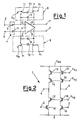
- Fig. 1 shows a completely differential SC filter of the first order, which in a mode known in itself (say, in the US Patent No. 4,609,877 and in the European Patent Application No. 0293020 by the same Applicant) comprises an operational amplifier 1 having two inputs 2 connected to respective signal inputs 3 by means of a connecting network 4 formed by condensers 5, as well as two outputs 6 directly connected to respective signal outputs 7.
- Outputs 6 of operational amplifier 1 are connected to inputs 2 of the same amplifier by means of respective negative feedback circuits 8, each of which consists of a first condenser 9 constantly connected between output 6 and input 2 and of a second condenser 10 alternatively connected between a terminal of polarization voltage Vp and a terminal of reference voltage Vr according to the position of a pair of switches 11.
- switches 11 in the position illustrated by a continuous line condensers 10 are suitably charged at a voltage Vp-Vr, while in the subsequent phase with the switches 11 in the position illustrated by a dotted line condensers 10 are connected in parallel with condensers 9.
- the filter according to the invention distinguishes itself in that the completely differential operational amplifier 1 does not include the usual common-mode feedback circuit.
- a suitable operational amplifier circuit accomplished with CMOS technology can thus be that of Fig. 2, which comprises two circuit branches 12 connected in parallel between a power supply source Vdd and ground and comprising, each, the series of two P-channel CMOS transistors 13 and 14 and two N-channel CMOS transistors 15 and 16.
- Transistors 13, 14 and 15 have their gates connected to respective polarizations Vb1, Vb2 and Vb3, transistors 16 have their gates connected to inputs 2 and intermediate branch points between transistors 14 and 15 are connected to outputs 6.
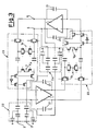
- an operational amplifier like that of Fig. 2 or analogous, that is, without a CMFB circuit, may be used for each of the two completely differential operational amplifiers 1, included in the second-order band-pass filter of Fig. 3.
- the filter of Fig. 3 also known in itself except for the type of operational amplifier used, comprises two amplifiers 1, each with two feedback condensers 21, an input coupling circuit 22 of the capacitative type, two switched-capacity circuits 23 with MOS transistors and capacities having polarization voltage Vp and reference voltage Vr and a multiplier circuit 24 of the capacitative type.
- the two circuits 23 and one of the amplifiers 1 form the differential feedback network for the other amplifier 1, also performing for it the same function of the common-mode feedback. More precisely, the common-mode output of each operational amplifier is forced towards the reference voltage Vr, which must be selected so as to be half the power supply voltage so as to optimize the output dynamics and must be ref erenced to the negative power supply so as to improve the power supply's differential suppression ratio for the same negative power supply.
- Vr reference voltage
Landscapes
- Engineering & Computer Science (AREA)
- Power Engineering (AREA)
- Amplifiers (AREA)
- Filters That Use Time-Delay Elements (AREA)
Abstract
Description
- The present invention relates to a completely differential filter with switched condensers using CMOS operational amplifiers with no common-mode feedback.
- The switched condenser technique (hereinafter called SC) represents the most popular analog approach for the implementation of high-precision filtering functions in commercial-type integrated circuits. The main reasons for the success of the SC technique are the following: a) resistors of large size can be replaced with very small switched condensers; b) it is possible to accomplish very accurate filtering time constants, given that they depend on capacitative ratios which are very well controlled in integrated circuits and on a clock frequency which can be generated accurately by a crystal oscillator.
- Up to now this technique has been shown to be effective in accomplishing audio band filters and there is now great demand to extend it to frequencies above the audio range, up to video band frequencies, for intermediate frequency filtering devices in heterodyne and double-heterodyne systems and television products for the consumer. The maximum central frequencies (in the case of band-pass or band-stop filters) and of band-limit frequencies (in the case of low-pass or high-pass filters) obtainable in SC filters are limited by the ability of the operational amplifiers used in the above filters to attain the desired final value within half a clock period. As a consequence, high-frequency filters always require operational amplifiers with a wide unit-gain bandwidth, a high direct current open-mesh gain (for applications having a high Q value) and a good slew rate.
- A second important request in the accomplishment of SC filters consists in the use of a supply voltage of 5V, so as to take advantage of technological progress and of analog/digital compatibility. Thus the dynamic field and the suppression of the power supply are also highly important design parameters.
- Recently, high-frequency filters with a high Q value have been accomplished successfully by selecting very simple topologies and a completely differential structure of the operational amplifier and exploiting recent technological improvements related to short-channel processes. Completely differential operational amplifiers are preferred over their unbalanced counterparts because they determine a wider dynamic field and a greater suppression of noise due to the power supply and to the clock signal passage. The main disadvantages of the completely differential approach consist, on the other hand, in the greater demand for area and for power due to the common-mode feedback circuit (hereinafter called CMFB) of the operational amplifier and in the limitation of the filtering rate due to the load of the CMFB circuit on the differential path.
- In view of this state of the art, the object of the present invention is to accomplish a completely differential filter, suitable for implementation in an integrated circuit, which does not suffer from the drawbacks indicated above due to the common mode feedback circuit of the operational amplifier.
- According to the invention such object is attained with a filter comprising at least one completely differential operational amplifier having two inputs and two outputs and at least one pair of feedback circuits of the differential signal arranged to connect said outputs with respective inputs of said amplifier outside of same, characterized in that said operational amplifier has no common-mode feedback circuit and in that the latter's function is performed by said pair of feedback circuits external to said amplifier.
- In this way the drawbacks mentioned above due to the operational amplifier's CAB circuits are overcome without losing the indispensable common-mode feedback function. This allows the accomplishment of a completely differential filter having a smaller area, reduced power dissipation, greater rates of operation and a greater dynamic field.
- The characteristics of the present invention shall be made evident to a greater extent by the following detailed description of its embodiments illustrated, as non-limiting examples, in the enclosed drawings, wherein:
- Fig. 1 shows the overall block diagram of a completely differential filter of the first order, accomplished according to the invention;
- Fig. 2 shows the circuit details of a possible CMOS operational amplifier included in the filter of Fig. 1;
- Fig. 3 shows a unit consisting of a completely differential band-pass filter of the second order, accomplished according to the invention.
- Fig. 1 shows a completely differential SC filter of the first order, which in a mode known in itself (say, in the US Patent No. 4,609,877 and in the European Patent Application No. 0293020 by the same Applicant) comprises an
operational amplifier 1 having twoinputs 2 connected torespective signal inputs 3 by means of a connecting network 4 formed bycondensers 5, as well as twooutputs 6 directly connected to respective signal outputs 7. -
Outputs 6 ofoperational amplifier 1 are connected toinputs 2 of the same amplifier by means of respective negative feedback circuits 8, each of which consists of afirst condenser 9 constantly connected betweenoutput 6 andinput 2 and of asecond condenser 10 alternatively connected between a terminal of polarization voltage Vp and a terminal of reference voltage Vr according to the position of a pair ofswitches 11. - With
switches 11 in the position illustrated by acontinuous line condensers 10 are suitably charged at a voltage Vp-Vr, while in the subsequent phase with theswitches 11 in the position illustrated by adotted line condensers 10 are connected in parallel withcondensers 9. - The manner of operation of the filter of Fig. 1 and of its variations is described in the US Patent and in the European Patent Application mentioned above.
- With respect to such known solutions, however, the filter according to the invention distinguishes itself in that the completely differential
operational amplifier 1 does not include the usual common-mode feedback circuit. - Such function, in fact, is performed by the same negative feedback circuits 8 already normally present in the filter.
- A suitable operational amplifier circuit accomplished with CMOS technology can thus be that of Fig. 2, which comprises two circuit branches 12 connected in parallel between a power supply source Vdd and ground and comprising, each, the series of two P-
channel CMOS transistors channel CMOS transistors Transistors transistors 16 have their gates connected toinputs 2 and intermediate branch points betweentransistors outputs 6. - As an alternative to the use hypothesized in Fig. 1, an operational amplifier like that of Fig. 2 or analogous, that is, without a CMFB circuit, may be used for each of the two completely differential
operational amplifiers 1, included in the second-order band-pass filter of Fig. 3. - The filter of Fig. 3, also known in itself except for the type of operational amplifier used, comprises two
amplifiers 1, each with twofeedback condensers 21, aninput coupling circuit 22 of the capacitative type, two switched-capacity circuits 23 with MOS transistors and capacities having polarization voltage Vp and reference voltage Vr and amultiplier circuit 24 of the capacitative type. - It appears evident that the two
circuits 23 and one of theamplifiers 1 form the differential feedback network for theother amplifier 1, also performing for it the same function of the common-mode feedback. More precisely, the common-mode output of each operational amplifier is forced towards the reference voltage Vr, which must be selected so as to be half the power supply voltage so as to optimize the output dynamics and must be ref erenced to the negative power supply so as to improve the power supply's differential suppression ratio for the same negative power supply. This is a fundamental condition for utilizing operational amplifiers such as that of fig. 2 without amplifying the noise on the negative power supply at the filter' s output.
Claims (2)
Applications Claiming Priority (2)
| Application Number | Priority Date | Filing Date | Title |
|---|---|---|---|
| IT2305988 | 1988-12-22 | ||
| IT8823059A IT1227615B (en) | 1988-12-22 | 1988-12-22 | FILTER COMPLETELY DIFFERENTIAL WITH SWITCHED CAPACITORS USING OPERATIONAL AMPLIFIERS CMOS WITHOUT COMMON MODE FEEDBACK |
Publications (3)
| Publication Number | Publication Date |
|---|---|
| EP0375017A2 true EP0375017A2 (en) | 1990-06-27 |
| EP0375017A3 EP0375017A3 (en) | 1990-09-26 |
| EP0375017B1 EP0375017B1 (en) | 2005-06-01 |
Family
ID=11203348
Family Applications (1)
| Application Number | Title | Priority Date | Filing Date |
|---|---|---|---|
| EP89203109A Expired - Lifetime EP0375017B1 (en) | 1988-12-22 | 1989-12-07 | Fully differential filter with switched condensers using CMOS operational amplifiers with no common-mode feedback |
Country Status (5)
| Country | Link |
|---|---|
| US (2) | US5084683A (en) |
| EP (1) | EP0375017B1 (en) |
| JP (1) | JPH02219314A (en) |
| DE (1) | DE68929535D1 (en) |
| IT (1) | IT1227615B (en) |
Cited By (3)
| Publication number | Priority date | Publication date | Assignee | Title |
|---|---|---|---|---|
| US7071778B2 (en) | 2003-04-28 | 2006-07-04 | Sony Corporation | High-speed low-power dynamic current biased operational amplifier |
| EP2552018A1 (en) * | 2011-07-26 | 2013-01-30 | ST-Ericsson SA | Microphone preamplifier circuit |
| US9263993B2 (en) | 2014-04-22 | 2016-02-16 | Mediatek Inc. | Low pass filter with common-mode noise reduction |
Families Citing this family (12)
| Publication number | Priority date | Publication date | Assignee | Title |
|---|---|---|---|---|
| JPH07336169A (en) * | 1994-06-03 | 1995-12-22 | Youzan:Kk | Amplifier circuit |
| SE9903532D0 (en) * | 1999-09-28 | 1999-09-28 | Jiren Yuan | Versatile charge sampling circuits |
| US7339418B2 (en) * | 2004-08-17 | 2008-03-04 | National Instruments Corporation | Differential filter topology with dielectric absorption cancellation for a data acquisition device |
| JP2006121480A (en) * | 2004-10-22 | 2006-05-11 | Sony Corp | Sample hold circuit and pipeline AD converter using the same |
| JP2006121307A (en) * | 2004-10-20 | 2006-05-11 | Sony Corp | Sample hold circuit or AD converter using the same |
| US8195096B2 (en) * | 2006-07-13 | 2012-06-05 | Mediatek Inc. | Apparatus and method for enhancing DC offset correction speed of a radio device |
| ATE500649T1 (en) * | 2008-06-13 | 2011-03-15 | Zoran Corp | AMPLIFIER CIRCUIT |
| US8009071B2 (en) * | 2009-12-11 | 2011-08-30 | Zoran Corporation | Gain circuit |
| EP2466745A1 (en) | 2010-12-17 | 2012-06-20 | Dialog Semiconductor GmbH | Amplifier common-mode control methods |
| US9231542B1 (en) | 2014-11-24 | 2016-01-05 | Dialog Semiconductor (Uk) Limited | Amplifier common-mode control method |
| ITUB20159233A1 (en) * | 2015-12-23 | 2017-06-23 | St Microelectronics Srl | ELECTRONIC AMPLIFICATION CIRCUIT WITH REDUCED START-UP TIME FOR A SIGNAL INCLUDING COMPONENTS IN SQUARE |
| CN115065234B (en) * | 2022-08-15 | 2022-11-18 | 英彼森半导体(珠海)有限公司 | Analog filter framework working at various power supply voltages and filtering method |
Family Cites Families (6)
| Publication number | Priority date | Publication date | Assignee | Title |
|---|---|---|---|---|
| US4574250A (en) * | 1981-10-13 | 1986-03-04 | Intel Corporation | Switched capacitor filter utilizing a differential input and output circuit and method |
| US4533877A (en) * | 1983-12-29 | 1985-08-06 | At&T Bell Laboratories | Telecommunication operational amplifier |
| IT1213243B (en) * | 1984-11-12 | 1989-12-14 | Ates Componenti Elettron | DIFFERENTIAL STRUCTURE BUFFER CIRCUIT FOR MEASURING CAPACITIVE CHARGES. |
| IT1215374B (en) * | 1987-03-05 | 1990-02-08 | Sgs Microelettronica Spa | ACTIVE INTEGRATED ELECTRONIC FILTER WITH VERY LOW SENSITIVITY TO COMPONENTS 'AIR. |
| IT1203893B (en) * | 1987-04-14 | 1989-02-23 | Sgs Microelettronica Spa | HIGH PRECISION AMPLIFICATION CIRCUIT WITH SMALL DIMENSION AND LOW POWER CONSUMPTION FOR INTEGRATED CIRCUITS. |
| IT1220188B (en) * | 1987-12-11 | 1990-06-06 | Sgs Microelettronica Spa | COMMON MODE DETECTION AND CONTROL OF BALANCED AMPLIFIERS |
-
1988
- 1988-12-22 IT IT8823059A patent/IT1227615B/en active
-
1989
- 1989-12-07 DE DE68929535T patent/DE68929535D1/en not_active Expired - Lifetime
- 1989-12-07 EP EP89203109A patent/EP0375017B1/en not_active Expired - Lifetime
- 1989-12-19 JP JP1327478A patent/JPH02219314A/en active Pending
- 1989-12-19 US US07/453,921 patent/US5084683A/en not_active Ceased
-
1994
- 1994-01-28 US US08/189,576 patent/USRE35379E/en not_active Expired - Lifetime
Cited By (6)
| Publication number | Priority date | Publication date | Assignee | Title |
|---|---|---|---|---|
| US7071778B2 (en) | 2003-04-28 | 2006-07-04 | Sony Corporation | High-speed low-power dynamic current biased operational amplifier |
| EP2552018A1 (en) * | 2011-07-26 | 2013-01-30 | ST-Ericsson SA | Microphone preamplifier circuit |
| WO2013014009A1 (en) | 2011-07-26 | 2013-01-31 | St-Ericsson Sa | Microphone preamplifier circuit |
| US9554209B2 (en) | 2011-07-26 | 2017-01-24 | Optis Circuit Technology, Llc | Microphone preamplifier circuit |
| US9263993B2 (en) | 2014-04-22 | 2016-02-16 | Mediatek Inc. | Low pass filter with common-mode noise reduction |
| EP2937996A3 (en) * | 2014-04-22 | 2016-03-02 | MediaTek, Inc | Low pass filter with common-mode noise reduction |
Also Published As
| Publication number | Publication date |
|---|---|
| IT1227615B (en) | 1991-04-22 |
| US5084683A (en) | 1992-01-28 |
| IT8823059A0 (en) | 1988-12-22 |
| USRE35379E (en) | 1996-11-19 |
| DE68929535D1 (en) | 2005-07-07 |
| EP0375017B1 (en) | 2005-06-01 |
| EP0375017A3 (en) | 1990-09-26 |
| JPH02219314A (en) | 1990-08-31 |
Similar Documents
| Publication | Publication Date | Title |
|---|---|---|
| US5084683A (en) | Completely differential filter with switched condensers using cmos operational amplifiers with no common-mode feedback | |
| EP0851578B1 (en) | Filter circuit | |
| US6060935A (en) | Continuous time capacitor-tuner integrator | |
| EP0461922B1 (en) | Integration circuit | |
| JP3316038B2 (en) | Frequency tuning system for operational transconductance amplifier-capacitor pairs | |
| US6975171B2 (en) | Balanced amplifier and filter using the same | |
| JPH06164313A (en) | Quality-factor tuning system and current rectifier used for it | |
| US4731590A (en) | Circuits with multiple controlled gain elements | |
| KR100298090B1 (en) | Frequency dependent resistor | |
| US5880641A (en) | Apparatus for stabilizing cut-off frequency using a transconductance | |
| JPWO1997032396A1 (en) | Frequency Dependent Resistor | |
| US5216375A (en) | Variable time-constant type differentiator | |
| JP4272053B2 (en) | Linear amplifier using CMOS capacitor with non-linear characteristics | |
| US20050030092A1 (en) | Active filter circuit with operational amplifier | |
| US5594387A (en) | Amplifier circuit having nagative feedback loop for self-bias | |
| US7071760B2 (en) | Filter circuit and detection circuit having filter circuit | |
| US5177382A (en) | Active filter circuit | |
| US4644291A (en) | Operational amplifier | |
| JP3462408B2 (en) | DC feedback circuit | |
| JP3308352B2 (en) | Variable delay circuit | |
| JP2002330058A (en) | Gm-C FILTER | |
| JP3189751B2 (en) | Frequency adjustment device | |
| US6188272B1 (en) | Filter circuit | |
| JPH06152318A (en) | Filter circuit | |
| KR100413184B1 (en) | Switched-Capacitor circuit using inverting amplifier |
Legal Events
| Date | Code | Title | Description |
|---|---|---|---|
| PUAI | Public reference made under article 153(3) epc to a published international application that has entered the european phase |
Free format text: ORIGINAL CODE: 0009012 |
|
| AK | Designated contracting states |
Kind code of ref document: A2 Designated state(s): DE FR GB NL |
|
| PUAL | Search report despatched |
Free format text: ORIGINAL CODE: 0009013 |
|
| AK | Designated contracting states |
Kind code of ref document: A3 Designated state(s): DE FR GB NL |
|
| 17P | Request for examination filed |
Effective date: 19901213 |
|
| 17Q | First examination report despatched |
Effective date: 19930727 |
|
| RAP3 | Party data changed (applicant data changed or rights of an application transferred) |
Owner name: STMICROELECTRONICS S.R.L. |
|
| RTI1 | Title (correction) |
Free format text: FULLY DIFFERENTIAL FILTER WITH SWITCHED CONDENSERS USING CMOS OPERATIONAL AMPLIFIERS WITH NO COMMON-MODE FEEDBACK |
|
| GRAP | Despatch of communication of intention to grant a patent |
Free format text: ORIGINAL CODE: EPIDOSNIGR1 |
|
| GRAS | Grant fee paid |
Free format text: ORIGINAL CODE: EPIDOSNIGR3 |
|
| GRAA | (expected) grant |
Free format text: ORIGINAL CODE: 0009210 |
|
| AK | Designated contracting states |
Kind code of ref document: B1 Designated state(s): DE FR GB NL |
|
| PG25 | Lapsed in a contracting state [announced via postgrant information from national office to epo] |
Ref country code: NL Free format text: LAPSE BECAUSE OF FAILURE TO SUBMIT A TRANSLATION OF THE DESCRIPTION OR TO PAY THE FEE WITHIN THE PRESCRIBED TIME-LIMIT Effective date: 20050601 |
|
| REG | Reference to a national code |
Ref country code: GB Ref legal event code: FG4D |
|
| REF | Corresponds to: |
Ref document number: 68929535 Country of ref document: DE Date of ref document: 20050707 Kind code of ref document: P |
|
| PG25 | Lapsed in a contracting state [announced via postgrant information from national office to epo] |
Ref country code: DE Free format text: LAPSE BECAUSE OF FAILURE TO SUBMIT A TRANSLATION OF THE DESCRIPTION OR TO PAY THE FEE WITHIN THE PRESCRIBED TIME-LIMIT Effective date: 20050902 |
|
| NLV1 | Nl: lapsed or annulled due to failure to fulfill the requirements of art. 29p and 29m of the patents act | ||
| PLBE | No opposition filed within time limit |
Free format text: ORIGINAL CODE: 0009261 |
|
| STAA | Information on the status of an ep patent application or granted ep patent |
Free format text: STATUS: NO OPPOSITION FILED WITHIN TIME LIMIT |
|
| ET | Fr: translation filed | ||
| 26N | No opposition filed |
Effective date: 20060302 |
|
| PGFP | Annual fee paid to national office [announced via postgrant information from national office to epo] |
Ref country code: GB Payment date: 20061127 Year of fee payment: 18 |
|
| PGFP | Annual fee paid to national office [announced via postgrant information from national office to epo] |
Ref country code: FR Payment date: 20061228 Year of fee payment: 18 |
|
| GBPC | Gb: european patent ceased through non-payment of renewal fee |
Effective date: 20071207 |
|
| REG | Reference to a national code |
Ref country code: FR Ref legal event code: ST Effective date: 20081020 |
|
| PG25 | Lapsed in a contracting state [announced via postgrant information from national office to epo] |
Ref country code: GB Free format text: LAPSE BECAUSE OF NON-PAYMENT OF DUE FEES Effective date: 20071207 |
|
| PG25 | Lapsed in a contracting state [announced via postgrant information from national office to epo] |
Ref country code: FR Free format text: LAPSE BECAUSE OF NON-PAYMENT OF DUE FEES Effective date: 20071231 |