EP0374643A2 - Process for producing thin films - Google Patents
Process for producing thin films Download PDFInfo
- Publication number
- EP0374643A2 EP0374643A2 EP89122737A EP89122737A EP0374643A2 EP 0374643 A2 EP0374643 A2 EP 0374643A2 EP 89122737 A EP89122737 A EP 89122737A EP 89122737 A EP89122737 A EP 89122737A EP 0374643 A2 EP0374643 A2 EP 0374643A2
- Authority
- EP
- European Patent Office
- Prior art keywords
- thin films
- cathode
- hydrophobic substance
- surfactant
- electrode
- Prior art date
- Legal status (The legal status is an assumption and is not a legal conclusion. Google has not performed a legal analysis and makes no representation as to the accuracy of the status listed.)
- Withdrawn
Links
- 239000010409 thin film Substances 0.000 title claims abstract description 75
- 238000000034 method Methods 0.000 title claims description 47
- 229910052782 aluminium Inorganic materials 0.000 claims abstract description 48
- XAGFODPZIPBFFR-UHFFFAOYSA-N aluminium Chemical compound [Al] XAGFODPZIPBFFR-UHFFFAOYSA-N 0.000 claims abstract description 48
- 230000002209 hydrophobic effect Effects 0.000 claims abstract description 43
- 239000000126 substance Substances 0.000 claims abstract description 42
- 239000004094 surface-active agent Substances 0.000 claims abstract description 23
- 239000010953 base metal Substances 0.000 claims abstract description 13
- 239000000843 powder Substances 0.000 claims abstract description 13
- 239000012736 aqueous medium Substances 0.000 claims abstract description 12
- 239000006185 dispersion Substances 0.000 claims abstract description 6
- 239000000693 micelle Substances 0.000 claims description 55
- -1 polyoxyethylene Polymers 0.000 claims description 38
- KTWOOEGAPBSYNW-UHFFFAOYSA-N ferrocene Chemical group [Fe+2].C=1C=C[CH-]C=1.C=1C=C[CH-]C=1 KTWOOEGAPBSYNW-UHFFFAOYSA-N 0.000 claims description 26
- 239000002800 charge carrier Substances 0.000 claims description 22
- 239000003795 chemical substances by application Substances 0.000 claims description 12
- 229920003171 Poly (ethylene oxide) Polymers 0.000 claims description 9
- 150000001875 compounds Chemical class 0.000 claims description 7
- 235000014113 dietary fatty acids Nutrition 0.000 claims description 6
- 229930195729 fatty acid Natural products 0.000 claims description 6
- 239000000194 fatty acid Substances 0.000 claims description 6
- 239000002245 particle Substances 0.000 claims description 6
- 239000007788 liquid Substances 0.000 claims description 5
- VEXZGXHMUGYJMC-UHFFFAOYSA-M Chloride anion Chemical compound [Cl-] VEXZGXHMUGYJMC-UHFFFAOYSA-M 0.000 claims description 3
- 150000005215 alkyl ethers Chemical class 0.000 claims description 3
- 125000005211 alkyl trimethyl ammonium group Chemical group 0.000 claims description 3
- 150000004665 fatty acids Chemical class 0.000 claims description 3
- UDGSVBYJWHOHNN-UHFFFAOYSA-N n',n'-diethylethane-1,2-diamine Chemical compound CCN(CC)CCN UDGSVBYJWHOHNN-UHFFFAOYSA-N 0.000 claims description 2
- 239000000463 material Substances 0.000 abstract description 21
- 239000000243 solution Substances 0.000 description 64
- BASFCYQUMIYNBI-UHFFFAOYSA-N platinum Chemical compound [Pt] BASFCYQUMIYNBI-UHFFFAOYSA-N 0.000 description 44
- AMXOYNBUYSYVKV-UHFFFAOYSA-M lithium bromide Chemical compound [Li+].[Br-] AMXOYNBUYSYVKV-UHFFFAOYSA-M 0.000 description 24
- IEQIEDJGQAUEQZ-UHFFFAOYSA-N phthalocyanine Chemical class N1C(N=C2C3=CC=CC=C3C(N=C3C4=CC=CC=C4C(=N4)N3)=N2)=C(C=CC=C2)C2=C1N=C1C2=CC=CC=C2C4=N1 IEQIEDJGQAUEQZ-UHFFFAOYSA-N 0.000 description 23
- 229910052697 platinum Inorganic materials 0.000 description 22
- 238000000862 absorption spectrum Methods 0.000 description 20
- 239000003792 electrolyte Substances 0.000 description 19
- XLYOFNOQVPJJNP-UHFFFAOYSA-N water Substances O XLYOFNOQVPJJNP-UHFFFAOYSA-N 0.000 description 17
- 239000010408 film Substances 0.000 description 16
- 239000000203 mixture Substances 0.000 description 16
- 238000005868 electrolysis reaction Methods 0.000 description 14
- 150000003839 salts Chemical class 0.000 description 14
- RBTKNAXYKSUFRK-UHFFFAOYSA-N heliogen blue Chemical compound [Cu].[N-]1C2=C(C=CC=C3)C3=C1N=C([N-]1)C3=CC=CC=C3C1=NC([N-]1)=C(C=CC=C3)C3=C1N=C([N-]1)C3=CC=CC=C3C1=N2 RBTKNAXYKSUFRK-UHFFFAOYSA-N 0.000 description 13
- 229920000642 polymer Polymers 0.000 description 13
- 238000003756 stirring Methods 0.000 description 13
- ZOMNIUBKTOKEHS-UHFFFAOYSA-L dimercury dichloride Chemical class Cl[Hg][Hg]Cl ZOMNIUBKTOKEHS-UHFFFAOYSA-L 0.000 description 12
- 229910052799 carbon Inorganic materials 0.000 description 10
- 238000004040 coloring Methods 0.000 description 10
- 238000000926 separation method Methods 0.000 description 10
- 239000006228 supernatant Substances 0.000 description 10
- 238000001228 spectrum Methods 0.000 description 9
- 239000011521 glass Substances 0.000 description 8
- 239000000758 substrate Substances 0.000 description 8
- 229910021397 glassy carbon Inorganic materials 0.000 description 7
- 229920003227 poly(N-vinyl carbazole) Polymers 0.000 description 7
- ODHXBMXNKOYIBV-UHFFFAOYSA-N triphenylamine Chemical compound C1=CC=CC=C1N(C=1C=CC=CC=1)C1=CC=CC=C1 ODHXBMXNKOYIBV-UHFFFAOYSA-N 0.000 description 7
- 230000000052 comparative effect Effects 0.000 description 6
- RAXXELZNTBOGNW-UHFFFAOYSA-N imidazole Natural products C1=CNC=N1 RAXXELZNTBOGNW-UHFFFAOYSA-N 0.000 description 6
- JFGQHAHJWJBOPD-UHFFFAOYSA-N 3-hydroxy-n-phenylnaphthalene-2-carboxamide Chemical compound OC1=CC2=CC=CC=C2C=C1C(=O)NC1=CC=CC=C1 JFGQHAHJWJBOPD-UHFFFAOYSA-N 0.000 description 5
- RYGMFSIKBFXOCR-UHFFFAOYSA-N Copper Chemical compound [Cu] RYGMFSIKBFXOCR-UHFFFAOYSA-N 0.000 description 5
- 125000004432 carbon atom Chemical group C* 0.000 description 5
- 229920001577 copolymer Polymers 0.000 description 5
- 229910052802 copper Inorganic materials 0.000 description 5
- 239000010949 copper Substances 0.000 description 5
- 125000002496 methyl group Chemical group [H]C([H])([H])* 0.000 description 5
- 229920000767 polyaniline Polymers 0.000 description 5
- IEQAICDLOKRSRL-UHFFFAOYSA-N 2-[2-[2-[2-[2-[2-[2-[2-[2-[2-[2-[2-[2-[2-[2-[2-[2-[2-[2-[2-[2-[2-(2-dodecoxyethoxy)ethoxy]ethoxy]ethoxy]ethoxy]ethoxy]ethoxy]ethoxy]ethoxy]ethoxy]ethoxy]ethoxy]ethoxy]ethoxy]ethoxy]ethoxy]ethoxy]ethoxy]ethoxy]ethoxy]ethoxy]ethoxy]ethanol Chemical compound CCCCCCCCCCCCOCCOCCOCCOCCOCCOCCOCCOCCOCCOCCOCCOCCOCCOCCOCCOCCOCCOCCOCCOCCOCCOCCOCCO IEQAICDLOKRSRL-UHFFFAOYSA-N 0.000 description 4
- UJOBWOGCFQCDNV-UHFFFAOYSA-N 9H-carbazole Chemical compound C1=CC=C2C3=CC=CC=C3NC2=C1 UJOBWOGCFQCDNV-UHFFFAOYSA-N 0.000 description 4
- DGAQECJNVWCQMB-PUAWFVPOSA-M Ilexoside XXIX Chemical class C[C@@H]1CC[C@@]2(CC[C@@]3(C(=CC[C@H]4[C@]3(CC[C@@H]5[C@@]4(CC[C@@H](C5(C)C)OS(=O)(=O)[O-])C)C)[C@@H]2[C@]1(C)O)C)C(=O)O[C@H]6[C@@H]([C@H]([C@@H]([C@H](O6)CO)O)O)O.[Na+] DGAQECJNVWCQMB-PUAWFVPOSA-M 0.000 description 4
- WHXSMMKQMYFTQS-UHFFFAOYSA-N Lithium Chemical class [Li] WHXSMMKQMYFTQS-UHFFFAOYSA-N 0.000 description 4
- FYYHWMGAXLPEAU-UHFFFAOYSA-N Magnesium Chemical class [Mg] FYYHWMGAXLPEAU-UHFFFAOYSA-N 0.000 description 4
- ZLMJMSJWJFRBEC-UHFFFAOYSA-N Potassium Chemical class [K] ZLMJMSJWJFRBEC-UHFFFAOYSA-N 0.000 description 4
- SMWDFEZZVXVKRB-UHFFFAOYSA-N Quinoline Chemical compound N1=CC=CC2=CC=CC=C21 SMWDFEZZVXVKRB-UHFFFAOYSA-N 0.000 description 4
- 125000000217 alkyl group Chemical group 0.000 description 4
- HUMNYLRZRPPJDN-UHFFFAOYSA-N benzaldehyde Chemical compound O=CC1=CC=CC=C1 HUMNYLRZRPPJDN-UHFFFAOYSA-N 0.000 description 4
- 239000011230 binding agent Substances 0.000 description 4
- 238000000151 deposition Methods 0.000 description 4
- 229910052744 lithium Inorganic materials 0.000 description 4
- 229910052749 magnesium Inorganic materials 0.000 description 4
- 239000011777 magnesium Chemical class 0.000 description 4
- 239000002184 metal Chemical class 0.000 description 4
- 229910052751 metal Inorganic materials 0.000 description 4
- 239000000049 pigment Substances 0.000 description 4
- 239000011591 potassium Chemical class 0.000 description 4
- 229910052700 potassium Inorganic materials 0.000 description 4
- 229910052701 rubidium Inorganic materials 0.000 description 4
- IGLNJRXAVVLDKE-UHFFFAOYSA-N rubidium atom Chemical class [Rb] IGLNJRXAVVLDKE-UHFFFAOYSA-N 0.000 description 4
- 239000011734 sodium Chemical class 0.000 description 4
- 229910052708 sodium Inorganic materials 0.000 description 4
- OYPRJOBELJOOCE-UHFFFAOYSA-N Calcium Chemical class [Ca] OYPRJOBELJOOCE-UHFFFAOYSA-N 0.000 description 3
- LFQSCWFLJHTTHZ-UHFFFAOYSA-N Ethanol Chemical compound CCO LFQSCWFLJHTTHZ-UHFFFAOYSA-N 0.000 description 3
- UFHFLCQGNIYNRP-UHFFFAOYSA-N Hydrogen Chemical compound [H][H] UFHFLCQGNIYNRP-UHFFFAOYSA-N 0.000 description 3
- PXHVJJICTQNCMI-UHFFFAOYSA-N Nickel Chemical compound [Ni] PXHVJJICTQNCMI-UHFFFAOYSA-N 0.000 description 3
- 239000004952 Polyamide Substances 0.000 description 3
- QVGXLLKOCUKJST-UHFFFAOYSA-N atomic oxygen Chemical compound [O] QVGXLLKOCUKJST-UHFFFAOYSA-N 0.000 description 3
- 229910052791 calcium Inorganic materials 0.000 description 3
- 239000011575 calcium Chemical class 0.000 description 3
- 238000006243 chemical reaction Methods 0.000 description 3
- 125000002147 dimethylamino group Chemical group [H]C([H])([H])N(*)C([H])([H])[H] 0.000 description 3
- 239000001257 hydrogen Substances 0.000 description 3
- 229910052739 hydrogen Inorganic materials 0.000 description 3
- 230000003287 optical effect Effects 0.000 description 3
- 125000005740 oxycarbonyl group Chemical group [*:1]OC([*:2])=O 0.000 description 3
- 239000001301 oxygen Substances 0.000 description 3
- 229910052760 oxygen Inorganic materials 0.000 description 3
- 229920002037 poly(vinyl butyral) polymer Polymers 0.000 description 3
- 229920002647 polyamide Polymers 0.000 description 3
- PYSRRFNXTXNWCD-UHFFFAOYSA-N 3-(2-phenylethenyl)furan-2,5-dione Chemical compound O=C1OC(=O)C(C=CC=2C=CC=CC=2)=C1 PYSRRFNXTXNWCD-UHFFFAOYSA-N 0.000 description 2
- CSCPPACGZOOCGX-UHFFFAOYSA-N Acetone Chemical compound CC(C)=O CSCPPACGZOOCGX-UHFFFAOYSA-N 0.000 description 2
- SIKJAQJRHWYJAI-UHFFFAOYSA-N Indole Chemical compound C1=CC=C2NC=CC2=C1 SIKJAQJRHWYJAI-UHFFFAOYSA-N 0.000 description 2
- XEEYBQQBJWHFJM-UHFFFAOYSA-N Iron Chemical compound [Fe] XEEYBQQBJWHFJM-UHFFFAOYSA-N 0.000 description 2
- 239000004721 Polyphenylene oxide Substances 0.000 description 2
- 239000004734 Polyphenylene sulfide Substances 0.000 description 2
- 229920001328 Polyvinylidene chloride Polymers 0.000 description 2
- WTKZEGDFNFYCGP-UHFFFAOYSA-N Pyrazole Chemical compound C=1C=NNC=1 WTKZEGDFNFYCGP-UHFFFAOYSA-N 0.000 description 2
- BQCADISMDOOEFD-UHFFFAOYSA-N Silver Chemical compound [Ag] BQCADISMDOOEFD-UHFFFAOYSA-N 0.000 description 2
- 229920000147 Styrene maleic anhydride Polymers 0.000 description 2
- FZWLAAWBMGSTSO-UHFFFAOYSA-N Thiazole Chemical compound C1=CSC=N1 FZWLAAWBMGSTSO-UHFFFAOYSA-N 0.000 description 2
- GWEVSGVZZGPLCZ-UHFFFAOYSA-N Titan oxide Chemical compound O=[Ti]=O GWEVSGVZZGPLCZ-UHFFFAOYSA-N 0.000 description 2
- MCMNRKCIXSYSNV-UHFFFAOYSA-N Zirconium dioxide Chemical compound O=[Zr]=O MCMNRKCIXSYSNV-UHFFFAOYSA-N 0.000 description 2
- 238000002835 absorbance Methods 0.000 description 2
- 125000000738 acetamido group Chemical group [H]C([H])([H])C(=O)N([H])[*] 0.000 description 2
- 125000003172 aldehyde group Chemical group 0.000 description 2
- 125000003342 alkenyl group Chemical group 0.000 description 2
- 125000003545 alkoxy group Chemical group 0.000 description 2
- 125000003277 amino group Chemical group 0.000 description 2
- MWPLVEDNUUSJAV-UHFFFAOYSA-N anthracene Chemical class C1=CC=CC2=CC3=CC=CC=C3C=C21 MWPLVEDNUUSJAV-UHFFFAOYSA-N 0.000 description 2
- 239000007864 aqueous solution Substances 0.000 description 2
- 230000015572 biosynthetic process Effects 0.000 description 2
- 125000003178 carboxy group Chemical group [H]OC(*)=O 0.000 description 2
- MVPPADPHJFYWMZ-UHFFFAOYSA-N chlorobenzene Chemical compound ClC1=CC=CC=C1 MVPPADPHJFYWMZ-UHFFFAOYSA-N 0.000 description 2
- 230000008021 deposition Effects 0.000 description 2
- 125000000664 diazo group Chemical group [N-]=[N+]=[*] 0.000 description 2
- PCHJSUWPFVWCPO-UHFFFAOYSA-N gold Chemical compound [Au] PCHJSUWPFVWCPO-UHFFFAOYSA-N 0.000 description 2
- 229910052737 gold Inorganic materials 0.000 description 2
- 239000010931 gold Substances 0.000 description 2
- 229910052736 halogen Inorganic materials 0.000 description 2
- 150000002367 halogens Chemical class 0.000 description 2
- 150000007857 hydrazones Chemical class 0.000 description 2
- 125000002887 hydroxy group Chemical group [H]O* 0.000 description 2
- 229910044991 metal oxide Inorganic materials 0.000 description 2
- 150000004706 metal oxides Chemical class 0.000 description 2
- 125000001160 methoxycarbonyl group Chemical group [H]C([H])([H])OC(*)=O 0.000 description 2
- 239000002736 nonionic surfactant Substances 0.000 description 2
- 229920000620 organic polymer Polymers 0.000 description 2
- 125000005702 oxyalkylene group Chemical group 0.000 description 2
- 239000003973 paint Substances 0.000 description 2
- QNGNSVIICDLXHT-UHFFFAOYSA-N para-ethylbenzaldehyde Natural products CCC1=CC=C(C=O)C=C1 QNGNSVIICDLXHT-UHFFFAOYSA-N 0.000 description 2
- 125000002080 perylenyl group Chemical group C1(=CC=C2C=CC=C3C4=CC=CC5=CC=CC(C1=C23)=C45)* 0.000 description 2
- CSHWQDPOILHKBI-UHFFFAOYSA-N peryrene Natural products C1=CC(C2=CC=CC=3C2=C2C=CC=3)=C3C2=CC=CC3=C1 CSHWQDPOILHKBI-UHFFFAOYSA-N 0.000 description 2
- 229920003229 poly(methyl methacrylate) Polymers 0.000 description 2
- 229920002239 polyacrylonitrile Polymers 0.000 description 2
- 229920000728 polyester Polymers 0.000 description 2
- 239000004926 polymethyl methacrylate Substances 0.000 description 2
- 229920006380 polyphenylene oxide Polymers 0.000 description 2
- 229920000069 polyphenylene sulfide Polymers 0.000 description 2
- 229920001296 polysiloxane Polymers 0.000 description 2
- 150000004032 porphyrins Chemical class 0.000 description 2
- DNXIASIHZYFFRO-UHFFFAOYSA-N pyrazoline Chemical compound C1CN=NC1 DNXIASIHZYFFRO-UHFFFAOYSA-N 0.000 description 2
- 229910052709 silver Inorganic materials 0.000 description 2
- 239000004332 silver Substances 0.000 description 2
- 125000001424 substituent group Chemical group 0.000 description 2
- FHCPAXDKURNIOZ-UHFFFAOYSA-N tetrathiafulvalene Chemical compound S1C=CSC1=C1SC=CS1 FHCPAXDKURNIOZ-UHFFFAOYSA-N 0.000 description 2
- 238000011282 treatment Methods 0.000 description 2
- AAAQKTZKLRYKHR-UHFFFAOYSA-N triphenylmethane Chemical compound C1=CC=CC=C1C(C=1C=CC=CC=1)C1=CC=CC=C1 AAAQKTZKLRYKHR-UHFFFAOYSA-N 0.000 description 2
- 238000001771 vacuum deposition Methods 0.000 description 2
- KAEZRSFWWCTVNP-UHFFFAOYSA-N (4-methoxyphenyl)-(4-methoxyphenyl)imino-oxidoazanium Chemical compound C1=CC(OC)=CC=C1N=[N+]([O-])C1=CC=C(OC)C=C1 KAEZRSFWWCTVNP-UHFFFAOYSA-N 0.000 description 1
- OCJBOOLMMGQPQU-UHFFFAOYSA-N 1,4-dichlorobenzene Chemical compound ClC1=CC=C(Cl)C=C1 OCJBOOLMMGQPQU-UHFFFAOYSA-N 0.000 description 1
- JTPNRXUCIXHOKM-UHFFFAOYSA-N 1-chloronaphthalene Chemical compound C1=CC=C2C(Cl)=CC=CC2=C1 JTPNRXUCIXHOKM-UHFFFAOYSA-N 0.000 description 1
- NOEWOXIQPYAWCG-UHFFFAOYSA-L 1-dodecyl-4-(1-dodecylpyridin-1-ium-4-yl)pyridin-1-ium;dibromide Chemical compound [Br-].[Br-].C1=C[N+](CCCCCCCCCCCC)=CC=C1C1=CC=[N+](CCCCCCCCCCCC)C=C1 NOEWOXIQPYAWCG-UHFFFAOYSA-L 0.000 description 1
- VRXAJMCFEOESJO-UHFFFAOYSA-L 1-heptyl-4-(1-heptylpyridin-1-ium-4-yl)pyridin-1-ium;dibromide Chemical compound [Br-].[Br-].C1=C[N+](CCCCCCC)=CC=C1C1=CC=[N+](CCCCCCC)C=C1 VRXAJMCFEOESJO-UHFFFAOYSA-L 0.000 description 1
- GTZCNONABJSHNM-UHFFFAOYSA-N 5,10,15,20-tetraphenyl-21,23-dihydroporphyrin zinc Chemical compound [Zn].c1cc2nc1c(-c1ccccc1)c1ccc([nH]1)c(-c1ccccc1)c1ccc(n1)c(-c1ccccc1)c1ccc([nH]1)c2-c1ccccc1 GTZCNONABJSHNM-UHFFFAOYSA-N 0.000 description 1
- QGZKDVFQNNGYKY-UHFFFAOYSA-O Ammonium Chemical compound [NH4+] QGZKDVFQNNGYKY-UHFFFAOYSA-O 0.000 description 1
- WKBOTKDWSSQWDR-UHFFFAOYSA-N Bromine atom Chemical compound [Br] WKBOTKDWSSQWDR-UHFFFAOYSA-N 0.000 description 1
- NLZUEZXRPGMBCV-UHFFFAOYSA-N Butylhydroxytoluene Chemical compound CC1=CC(C(C)(C)C)=C(O)C(C(C)(C)C)=C1 NLZUEZXRPGMBCV-UHFFFAOYSA-N 0.000 description 1
- 239000004215 Carbon black (E152) Substances 0.000 description 1
- ZAMOUSCENKQFHK-UHFFFAOYSA-N Chlorine atom Chemical compound [Cl] ZAMOUSCENKQFHK-UHFFFAOYSA-N 0.000 description 1
- PXGOKWXKJXAPGV-UHFFFAOYSA-N Fluorine Chemical compound FF PXGOKWXKJXAPGV-UHFFFAOYSA-N 0.000 description 1
- 235000000177 Indigofera tinctoria Nutrition 0.000 description 1
- CERQOIWHTDAKMF-UHFFFAOYSA-N Methacrylic acid Chemical compound CC(=C)C(O)=O CERQOIWHTDAKMF-UHFFFAOYSA-N 0.000 description 1
- VVQNEPGJFQJSBK-UHFFFAOYSA-N Methyl methacrylate Chemical compound COC(=O)C(C)=C VVQNEPGJFQJSBK-UHFFFAOYSA-N 0.000 description 1
- 206010034972 Photosensitivity reaction Diseases 0.000 description 1
- 239000004698 Polyethylene Substances 0.000 description 1
- 229920000265 Polyparaphenylene Polymers 0.000 description 1
- 239000004743 Polypropylene Substances 0.000 description 1
- 239000004793 Polystyrene Substances 0.000 description 1
- NRCMAYZCPIVABH-UHFFFAOYSA-N Quinacridone Chemical compound N1C2=CC=CC=C2C(=O)C2=C1C=C1C(=O)C3=CC=CC=C3NC1=C2 NRCMAYZCPIVABH-UHFFFAOYSA-N 0.000 description 1
- 229910052581 Si3N4 Inorganic materials 0.000 description 1
- MRQIXHXHHPWVIL-ISLYRVAYSA-N Sudan I Chemical compound OC1=CC=C2C=CC=CC2=C1\N=N\C1=CC=CC=C1 MRQIXHXHHPWVIL-ISLYRVAYSA-N 0.000 description 1
- QAOWNCQODCNURD-UHFFFAOYSA-N Sulfuric acid Chemical class OS(O)(=O)=O QAOWNCQODCNURD-UHFFFAOYSA-N 0.000 description 1
- 229910003069 TeO2 Inorganic materials 0.000 description 1
- ATJFFYVFTNAWJD-UHFFFAOYSA-N Tin Chemical compound [Sn] ATJFFYVFTNAWJD-UHFFFAOYSA-N 0.000 description 1
- HCHKCACWOHOZIP-UHFFFAOYSA-N Zinc Chemical compound [Zn] HCHKCACWOHOZIP-UHFFFAOYSA-N 0.000 description 1
- SMEGJBVQLJJKKX-HOTMZDKISA-N [(2R,3S,4S,5R,6R)-5-acetyloxy-3,4,6-trihydroxyoxan-2-yl]methyl acetate Chemical compound CC(=O)OC[C@@H]1[C@H]([C@@H]([C@H]([C@@H](O1)O)OC(=O)C)O)O SMEGJBVQLJJKKX-HOTMZDKISA-N 0.000 description 1
- CQHKDHVZYZUZMJ-UHFFFAOYSA-N [2,2-bis(hydroxymethyl)-3-prop-2-enoyloxypropyl] prop-2-enoate Chemical compound C=CC(=O)OCC(CO)(CO)COC(=O)C=C CQHKDHVZYZUZMJ-UHFFFAOYSA-N 0.000 description 1
- 238000010521 absorption reaction Methods 0.000 description 1
- 125000000218 acetic acid group Chemical class C(C)(=O)* 0.000 description 1
- 229940081735 acetylcellulose Drugs 0.000 description 1
- 150000008051 alkyl sulfates Chemical class 0.000 description 1
- 125000002947 alkylene group Chemical group 0.000 description 1
- 239000000956 alloy Substances 0.000 description 1
- 229910045601 alloy Inorganic materials 0.000 description 1
- PNEYBMLMFCGWSK-UHFFFAOYSA-N aluminium oxide Inorganic materials [O-2].[O-2].[O-2].[Al+3].[Al+3] PNEYBMLMFCGWSK-UHFFFAOYSA-N 0.000 description 1
- PYKYMHQGRFAEBM-UHFFFAOYSA-N anthraquinone Chemical class CCC(=O)c1c(O)c2C(=O)C3C(C=CC=C3O)C(=O)c2cc1CC(=O)OC PYKYMHQGRFAEBM-UHFFFAOYSA-N 0.000 description 1
- 150000004056 anthraquinones Chemical class 0.000 description 1
- 229910052788 barium Inorganic materials 0.000 description 1
- DSAJWYNOEDNPEQ-UHFFFAOYSA-N barium atom Chemical class [Ba] DSAJWYNOEDNPEQ-UHFFFAOYSA-N 0.000 description 1
- BNZLJNRQXPJPJY-UHFFFAOYSA-L barium(2+) 4-[(5-chloro-4-methyl-2-sulfophenyl)diazenyl]-3-oxidonaphthalene-2-carboxylate Chemical compound CC1=CC(=C(C=C1Cl)N=NC2=C(C(=CC3=CC=CC=C32)C(=O)[O-])[O-])S(=O)(=O)O.[Ba+2] BNZLJNRQXPJPJY-UHFFFAOYSA-L 0.000 description 1
- 229910052790 beryllium Inorganic materials 0.000 description 1
- ATBAMAFKBVZNFJ-UHFFFAOYSA-N beryllium atom Chemical class [Be] ATBAMAFKBVZNFJ-UHFFFAOYSA-N 0.000 description 1
- GDTBXPJZTBHREO-UHFFFAOYSA-N bromine Substances BrBr GDTBXPJZTBHREO-UHFFFAOYSA-N 0.000 description 1
- 229910052794 bromium Inorganic materials 0.000 description 1
- 238000005266 casting Methods 0.000 description 1
- 229920002301 cellulose acetate Polymers 0.000 description 1
- 238000005119 centrifugation Methods 0.000 description 1
- 238000005229 chemical vapour deposition Methods 0.000 description 1
- 239000000460 chlorine Substances 0.000 description 1
- 229910052801 chlorine Inorganic materials 0.000 description 1
- XCJYREBRNVKWGJ-UHFFFAOYSA-N copper(II) phthalocyanine Chemical compound [Cu+2].C12=CC=CC=C2C(N=C2[N-]C(C3=CC=CC=C32)=N2)=NC1=NC([C]1C=CC=CC1=1)=NC=1N=C1[C]3C=CC=CC3=C2[N-]1 XCJYREBRNVKWGJ-UHFFFAOYSA-N 0.000 description 1
- 229910052593 corundum Inorganic materials 0.000 description 1
- 239000002537 cosmetic Substances 0.000 description 1
- 229910052955 covellite Inorganic materials 0.000 description 1
- 238000010908 decantation Methods 0.000 description 1
- 229940117389 dichlorobenzene Drugs 0.000 description 1
- 239000000975 dye Substances 0.000 description 1
- 230000005611 electricity Effects 0.000 description 1
- 230000005518 electrochemistry Effects 0.000 description 1
- 230000007613 environmental effect Effects 0.000 description 1
- 125000001495 ethyl group Chemical group [H]C([H])([H])C([H])([H])* 0.000 description 1
- 125000000816 ethylene group Chemical group [H]C([H])([*:1])C([H])([H])[*:2] 0.000 description 1
- 229910052731 fluorine Inorganic materials 0.000 description 1
- 239000011737 fluorine Substances 0.000 description 1
- 235000013305 food Nutrition 0.000 description 1
- 230000006870 function Effects 0.000 description 1
- 239000007789 gas Substances 0.000 description 1
- 150000004820 halides Chemical class 0.000 description 1
- 238000010438 heat treatment Methods 0.000 description 1
- 239000007970 homogeneous dispersion Substances 0.000 description 1
- 229930195733 hydrocarbon Natural products 0.000 description 1
- 150000002430 hydrocarbons Chemical class 0.000 description 1
- 229940097275 indigo Drugs 0.000 description 1
- COHYTHOBJLSHDF-UHFFFAOYSA-N indigo powder Natural products N1C2=CC=CC=C2C(=O)C1=C1C(=O)C2=CC=CC=C2N1 COHYTHOBJLSHDF-UHFFFAOYSA-N 0.000 description 1
- 229910003437 indium oxide Inorganic materials 0.000 description 1
- PJXISJQVUVHSOJ-UHFFFAOYSA-N indium(iii) oxide Chemical compound [O-2].[O-2].[O-2].[In+3].[In+3] PJXISJQVUVHSOJ-UHFFFAOYSA-N 0.000 description 1
- 230000002401 inhibitory effect Effects 0.000 description 1
- PNDPGZBMCMUPRI-UHFFFAOYSA-N iodine Chemical compound II PNDPGZBMCMUPRI-UHFFFAOYSA-N 0.000 description 1
- 238000010884 ion-beam technique Methods 0.000 description 1
- 229910052742 iron Inorganic materials 0.000 description 1
- JEIPFZHSYJVQDO-UHFFFAOYSA-N iron(III) oxide Inorganic materials O=[Fe]O[Fe]=O JEIPFZHSYJVQDO-UHFFFAOYSA-N 0.000 description 1
- 239000004973 liquid crystal related substance Substances 0.000 description 1
- 239000012528 membrane Substances 0.000 description 1
- 125000000956 methoxy group Chemical group [H]C([H])([H])O* 0.000 description 1
- 238000001451 molecular beam epitaxy Methods 0.000 description 1
- 125000000896 monocarboxylic acid group Chemical group 0.000 description 1
- 229910052759 nickel Inorganic materials 0.000 description 1
- 239000011368 organic material Substances 0.000 description 1
- 239000003960 organic solvent Substances 0.000 description 1
- 230000033116 oxidation-reduction process Effects 0.000 description 1
- 125000006353 oxyethylene group Chemical group 0.000 description 1
- 230000036211 photosensitivity Effects 0.000 description 1
- 238000005268 plasma chemical vapour deposition Methods 0.000 description 1
- 230000010287 polarization Effects 0.000 description 1
- 229920000515 polycarbonate Polymers 0.000 description 1
- 239000004417 polycarbonate Substances 0.000 description 1
- 229920000573 polyethylene Polymers 0.000 description 1
- 229920001246 polyethylene glycol monostearate Polymers 0.000 description 1
- 229920000259 polyoxyethylene lauryl ether Polymers 0.000 description 1
- 229920002503 polyoxyethylene-polyoxypropylene Polymers 0.000 description 1
- 229920001155 polypropylene Polymers 0.000 description 1
- 229920000128 polypyrrole Polymers 0.000 description 1
- 229920002223 polystyrene Polymers 0.000 description 1
- 229920000123 polythiophene Polymers 0.000 description 1
- 229920002689 polyvinyl acetate Polymers 0.000 description 1
- 239000011118 polyvinyl acetate Substances 0.000 description 1
- 238000002360 preparation method Methods 0.000 description 1
- 125000004805 propylene group Chemical group [H]C([H])([H])C([H])([*:1])C([H])([H])[*:2] 0.000 description 1
- 238000004062 sedimentation Methods 0.000 description 1
- 239000004065 semiconductor Substances 0.000 description 1
- 239000002904 solvent Substances 0.000 description 1
- 229910052950 sphalerite Inorganic materials 0.000 description 1
- 238000004528 spin coating Methods 0.000 description 1
- 239000010935 stainless steel Substances 0.000 description 1
- 229910001220 stainless steel Inorganic materials 0.000 description 1
- 239000007858 starting material Substances 0.000 description 1
- 230000003068 static effect Effects 0.000 description 1
- 229910052712 strontium Inorganic materials 0.000 description 1
- CIOAGBVUUVVLOB-UHFFFAOYSA-N strontium atom Chemical class [Sr] CIOAGBVUUVVLOB-UHFFFAOYSA-N 0.000 description 1
- LAJZODKXOMJMPK-UHFFFAOYSA-N tellurium dioxide Chemical compound O=[Te]=O LAJZODKXOMJMPK-UHFFFAOYSA-N 0.000 description 1
- YNHJECZULSZAQK-UHFFFAOYSA-N tetraphenylporphyrin Chemical compound C1=CC(C(=C2C=CC(N2)=C(C=2C=CC=CC=2)C=2C=CC(N=2)=C(C=2C=CC=CC=2)C2=CC=C3N2)C=2C=CC=CC=2)=NC1=C3C1=CC=CC=C1 YNHJECZULSZAQK-UHFFFAOYSA-N 0.000 description 1
- JOUDBUYBGJYFFP-FOCLMDBBSA-N thioindigo Chemical compound S\1C2=CC=CC=C2C(=O)C/1=C1/C(=O)C2=CC=CC=C2S1 JOUDBUYBGJYFFP-FOCLMDBBSA-N 0.000 description 1
- 229910052718 tin Inorganic materials 0.000 description 1
- 239000011135 tin Substances 0.000 description 1
- XOLBLPGZBRYERU-UHFFFAOYSA-N tin dioxide Chemical compound O=[Sn]=O XOLBLPGZBRYERU-UHFFFAOYSA-N 0.000 description 1
- 229910001887 tin oxide Inorganic materials 0.000 description 1
- 230000009466 transformation Effects 0.000 description 1
- 229910052720 vanadium Inorganic materials 0.000 description 1
- 238000005406 washing Methods 0.000 description 1
- 229920003176 water-insoluble polymer Polymers 0.000 description 1
- 229910001845 yogo sapphire Inorganic materials 0.000 description 1
- 229910052725 zinc Inorganic materials 0.000 description 1
- 239000011701 zinc Substances 0.000 description 1
- 229910052984 zinc sulfide Inorganic materials 0.000 description 1
Images


Classifications
-
- G—PHYSICS
- G03—PHOTOGRAPHY; CINEMATOGRAPHY; ANALOGOUS TECHNIQUES USING WAVES OTHER THAN OPTICAL WAVES; ELECTROGRAPHY; HOLOGRAPHY
- G03G—ELECTROGRAPHY; ELECTROPHOTOGRAPHY; MAGNETOGRAPHY
- G03G5/00—Recording members for original recording by exposure, e.g. to light, to heat, to electrons; Manufacture thereof; Selection of materials therefor
- G03G5/02—Charge-receiving layers
- G03G5/04—Photoconductive layers; Charge-generation layers or charge-transporting layers; Additives therefor; Binders therefor
- G03G5/05—Organic bonding materials; Methods for coating a substrate with a photoconductive layer; Inert supplements for use in photoconductive layers
- G03G5/0525—Coating methods
Definitions
- the present invention relates to a process for producing thin films, and more particularly to a process for efficiently producing thin films which are tightly sticking to cathodes consisting of base metals such as aluminum and the like.
- the vacuum deposition method For producing thin films including coloring matter, there have heretofore been known the vacuum deposition method, the heat CVD method, the plasma CVD method, the ultrahigh vacuum (ion beam, molecular beam epitaxy) method, the LB membrane method and the casting method.
- the object of the present invention is to provide a process for forming thin films which are uniform and tightly sticking to base metals.
- Another object of the present invention is to provide a process for efficiently producing an excellent photoconductor for electrophotography.
- the present invention is to provide a process for producing a thin film, characterized by electrotreating a dispersion or solution obtained by dispersing or dissolving hydrophobic substance powder in an aqueous medium with a surfactant having a HLB value of 10.0 to 20.0 under the conditions for forming thin films of abovementioned hydrophobic substances on a cathode.
- hydrophobic substance powder is applied as the material of thin films.
- the average particle diameter of said hydrophobic substance powder is preferably not more than 10 ⁇ m, particularly 1 to 0.01 ⁇ m. If the average particle diameter is in excess of 10 ⁇ m, there may be caused various disadvantages that it takes much time to disperse or dissolve in aqueous medium or it is difficult to disperse or dissolve homogeneously.
- the kind of said hydrophobic substance powder may be selected properly according to the uses of thin films to be formed, and various ones can be used irrespective of organic substance or inorganic substance.
- coloring matters for optical memory are coloring matters for optical memory and organic coloring matters such as perylene, indigo, thioindigo, squalilium, dichlorobenzene, thiapyrylium, azo-type coloring matter, quinacridone, viologen, Sudan, lake pigment, phthalocyanine blue, photalocyanine green, anthracene, anthraquinone, phthalocyanine, metal complexes of phthalocyanine, derivatives thereof, porphyrin, metal complexes of porphyrin, and derivatives thereof; electrochromic materials such as 1,1′-diheptyl-4,4′-bipyridinium dibromide, 1,1′-didodecyl-4,4′-bipyridinium dibromide and the like, lightsensitive materials (photochro
- hydrophobic compounds among the coloring matters each for electronics, recording, photo-chromism, photos, energy use, biomedicals, and coloring matters for food and cosmetics, dyes, coloring matters for specific coloring which are listed in "Color Chemical Cyclopedia", CMC Co., Ltd., pp542 - 717, March 28, 1988.
- Particularly preferred among the above are metal complexes and derivatives of phthalocyanine (Pc), specifically X-type and ⁇ -type H2-Pc, ⁇ -type, Cu-Pc, VO-Pc, InCl-Pc, AlCl-Pc, ⁇ -type TiO-Pc, Mg-Pc and the like.
- electrically conductive organic materials and gas sensor materials such as the 1:1 complex of 7,7,8,8-tetra-cyanoquinonedimethane (TCNQ) and tetrathiafulvalene (TTF), light curing paints such as pentaerythritol diacrylate and the like, diazo-type lightsensitive materials and paints such as 1-phenylazo-2-naphthol and the like can be used.
- TCNQ 7,7,8,8-tetra-cyanoquinonedimethane
- TTF tetrathiafulvalene
- light curing paints such as pentaerythritol diacrylate and the like
- diazo-type lightsensitive materials and paints such as 1-phenylazo-2-naphthol and the like
- water-insoluble polymers including general purpose polymers such as polycarbonate, polystyrene, polyethylene, polypropylene polyamide, polyphenylene sulfide (PPS), polyphenylene oxide (PPO), polyacrylonitrile (PAN) and the like; polyphenylene, polypyrrole, polyaniline, polythiophene, acetyl cellulose, poly(vinyl acetate), poly(vinyl butyral), and various polymers (poly(vinyl pyridine) and the like) and copolymers (copolymer of methyl methacrylate and methacrylic acid and the like) can be used.
- general purpose polymers such as polycarbonate, polystyrene, polyethylene, polypropylene polyamide, polyphenylene sulfide (PPS), polyphenylene oxide (PPO), polyacrylonitrile (PAN) and the like
- PPS polyphenylene sulfide
- PPO polyphenylene oxide
- the inorganic hydrophobic substances therein may extend to those of various kinds in various manners, including TiO2, C, CdS, WO3, Fe2O3, Y2O3 ZrO2 Al2O3, CuS, ZnS, TeO2, LiNb3O, Si3N4 and the like, and various kinds of superconductive oxides.
- CGM charge carrier generation materials
- preferable thin films as said photoconductor for electrophotography can be obtained.
- aqueous medium to be used in the present invention various media such as water, mixture of water and alcohol, mixture of water and acetone, and the like can be used.
- surfactants used in the present invention are the surfactants having HLB value of 10.0 to 20.0, preferably 12 to 18.
- Preferred example of such surfactants are non-ionic surfactants such as polyoxyethylene alkylether, polyoxyethylene fatty acid ester, polyoxyethylene alkylphenylether, polyoxyethylene polyoxypropylene alkylether and the like.
- alkyl sulfates, polyoxyethylene alkylether sulfates, alkyltrimethylammonium chloride, fatty acid diethylaminoethyl amide and the like can also be used.
- ferrocene derivatives can be also used.
- Said ferrocene derivatives include various kinds. Representative examples of them are ferrocene derivatives represented by the general formula: wherein, R1 and R2 are each an alkyl group having not more than 6 carbon atoms, an alkoxyl group having not more than 6 carbon atoms, an amino group, a dimethylamino group, a hydroxyl group, an acetyl amino group, a carboxyl group, a methoxycarbonyl group, an acetoxyl group, an aldehyde group and a halogen, R3 indicates a hydrogen or a straight chain or branched alkyl group or alkenyl group having 4 to 18 carbon atoms, and R4 and R5 indicate each a hydrogen or a methyl group.
- Y indicates an oxygen or an oxycarbonyl group
- a is an integer of 0 to 4
- b is an integer of 0 to 4
- m is an integer of 1 to 18, and
- n is a real number of 2.0 to 70.0.
- R1 and R2 are each an alkyl group (a methyl group (CH3), an ethyl group (C2H5), etc.), an alkoxyl group (a methoxyl group (OCH3), an ethoxyl group (OC2H5), etc.), an amino group (NH2), a dimethylamino group (N(CH3)2), a hydroxyl group (OH), an acetylamino group (NHCOCH3), a carboxyl group (COOH), an acetoxyl group (OCOCH3), a methoxycarbonyl group (COOCH3), an aldehyde group (CHO) or a halogen (a chlorine, a bromine, a fluorine, an iodine, etc.)
- R1 and R2 may be identical or different, and in case plural R1s and R2s exist in five-membered ring of ferrocene, plural substituents may be identical or different.
- R3 indicates
- Y indicates an oxygen (-O-) or an oxycarbonyl group (-C-O-), and R4 and R5 are each a hydrogen or a methyl group (CH3). Accordingly, or the like.
- n indicates an integer of 1 to 18. Accordingly, between the ring member carbon atoms and the abovedescribed oxygen or an oxycarbonyl group, an alkylene group having 1 to 18 carbon atoms such as an ethylene group, a propylene group and the like is interposed. Further, in indicates the repeating number of abovedescribed oxyalkylene group including oxyethylene group and the like, and means not only integers but also real number including them in the rang eof 2.0 to 70.0, showing the mean value of the repeating number of oxyalkylene group and the like.
- ferrocene derivatives represented by the above general formula (I) various ones including ammonium type and pyrridine type (International Patent Publication WO88/07538, etc.) can be used in the present invention.
- various ones including ammonium type and pyrridine type can be used in the present invention.
- further examples are the ferrocene derivatives described in the specifications of Japanese Patent Application Nos. 233797/1988, 233798/1988, 248600/1988, 248601/1988, 45370/1989, 54956/1989, 70680/1989, 70681/1989, 76498/1989 and 74699/1989.
- ferrocene derivatives can very efficiently dissolve or disperse hydrophobic substances into aqueous medium.
- one of the above surfactants and hydrophobic substance powder are added in an aqueous medium, and the mixture is stirred fully by the use of ultrasonic waves, homogenizer or stirrer for 1 hour to 7 days.
- the hydrophobic substance powder is homogeneously dispersed or dissolved in the aqueous medium by the function of surfactant having a HLB value of 10.0 to 20.0, to be dispersion or aqueous solution.
- hydrophobic substance powder may be supplementarily added to the electrolyte, or there may be provided a recycle circuit in which a part of electrolyte is withdrawn out of the system, the inorganic substance is added to the withdrawn electrolyte and thoroughly stirred, and then the resulting solution is returned to the system.
- the concentration of the surfactant in that process is not critical, but is usually selected in the range of 10 ⁇ M to 1 M, preferably 0.5 mM to 5 mM.
- concentration of it should be the threshold micelle concentration or higher.
- the supporting salt is added, if necessary, in order to control the electrical conductance of the aqueous medium.
- the amount of the supporting salt added is not critical as long as it does not inhibit the deposition of the hydrophobic substance dissolved or dispersed in the solution, but usually about 0 to 300 times and preferably about 10 to 200 times that of the above surfactant. Said supporting salt is not necessarily inevitable to electrotreatment. without it, a film of high purity containing no supporting salt can be obtained.
- the type of supporting salt is not critical as long as it is able to control the electric conductance for the aqueous medium without inhibiting the dissolving or deposition of the above hydrophobic substance onto the electrode.
- anodes are ITO (mixed oxide of indium oxide and tin oxide), platinum, gold, silver, glassy carbon, an electrically conductive metal oxide, an electrically conductive organic polymer and the like.
- cathodes are base metals including aluminum, zinc, tin, iron, nickel, magnesium and the like, and alloys including stainless steel and the like.
- copper, platinum, gold, silver, glassy carbon, electrically conductive metal oxide, an electrically conductive organic polymer and the like, semiconductors such as crystalline silicone, amorphous silicone and the like can be applied.
- a metal more noble than the oxidation-reduction potential (against +0.15 to +0.30 V saturated calomel electrode) of ferrocene derivatives, or an electrically conductive substance is used as the cathode.
- the potential on the cathode should be controlled to -0.03 to -10.0 V and in the electrotreatment with a galvanostat, the current density should be controlled in the range of 1 ⁇ A/cm2 to 100 mA/cm2.
- the liquid temperature is 0 to 50°C, preferably 5 to 40°C
- the potential of the cathode is -0.03 to -5.00 V, preferably -0.05 to -2.00 V.
- the current density should be 1 to 300 ⁇ A/cm2, preferably 1 to 100 ⁇ A/cm2.
- the thin films obtained according to the process of the present invention are effectively subjected to, if necessary, post treatments such as electrowashing, solvent washing, and baking treatment at 100 to 300°C.
- the thin film formed according to the process of the present invention are extensively and effectively used as the materials for optical disk, optical memory, photosensitive material, color filters, solar battery, toner, pigments and the like.
- charge carrier generation layer is formed on the cathode, as described before.
- it is effective to add an appropriate amount of binder polymer in the aqueous medium, if desired, to be included in the charge carrier generation layer to be formed, and heighten the mechanical strength of said layer.
- binder polymer to be used there poly(vinyl butyral), poly(methyl methacrylate), polyester, poly(vinylidene chloride), polyamide, styrene-maleic anhydride polymer and the like can be used.
- charge carrier transport material used for forming said charge carrier transport layer compounds such as indoline, quinoline, triphenylamine, bisazo, pyrazole, pyrazoline, oxidiazole, thiazole, imidazole, hydrazone, triphenylmethane, carbazole, benzaldehyde and the like or derivatives thereof, and polymers or copolymers containing these compounds or derivatives as substituents, or blends of the above compounds or derivatives and various polymer or copolymers.
- compounds such as indoline, quinoline, triphenylamine, bisazo, pyrazole, pyrazoline, oxidiazole, thiazole, imidazole, hydrazone, triphenylmethane, carbazole, benzaldehyde and the like or derivatives thereof, and polymers or copolymers containing these compounds or derivatives as substituents, or blends of the above compounds or derivatives and various polymer or copolymers.
- the reflection peak confirmed that the thin film on the aluminum (or platinum) substrate was made of phthalocyanine.
- micelle forming agent of ferrocene derivative represented by the structural formula 3 to make 2 mM.
- To 20 cc of micelle solution was added 0.1 g of copper phthalocyanine (produced by Dainichi Seika Co., Ltd.) and the resulting mixture was stirred by ultrasonic wave for 10 minutes to disperse and dissolve. After stirring with a stirrer 2 days and nights, obtained dispersed and soluble micelle solution was subjected to centrifugal separation for 30 minutes at 2000 rpm. A visible absorption spectrum of the supernatant confirmed that copper phthalocyanine was dispersed.
Landscapes
- Physics & Mathematics (AREA)
- General Physics & Mathematics (AREA)
- Photoreceptors In Electrophotography (AREA)
- Electrolytic Production Of Metals (AREA)
Abstract
Description
- The present invention relates to a process for producing thin films, and more particularly to a process for efficiently producing thin films which are tightly sticking to cathodes consisting of base metals such as aluminum and the like.
- For producing thin films including coloring matter, there have heretofore been known the vacuum deposition method, the heat CVD method, the plasma CVD method, the ultrahigh vacuum (ion beam, molecular beam epitaxy) method, the LB membrane method and the casting method.
- These methods, however, require the operations of dissolving the starting material such as coloring matters in organic solvents or heating them, so it has been impossible to form hydrophobic substances having little resistance to heat, into thin films.
- Recently, there have been developed the processes for forming thin films of various hydrophobic organic substances by use of so called Micellar Disruption Method (Electrochemistry Society, 54th Spring Convention F 201, 1987)(Japanese Patent Application Laid-Open No. 243298/1988).
- According to said Micellar Disruption Method, thin films of various hydrophobic substances can be efficiently produced, and said method has attracted attention as an industrially advantageous process. Thin films produced in this way are prospected for various uses such as color filter, photoelectric transformation materials and the like.
- According to the process disclosed here, however, though thin films can be formed on the anode, it has been very difficult to form films on base metals which dissolve easily by positive polarization.
- On the other hand, in the field of photosensitive materials, film forming on the substrates of base metals such as aluminum has been desired, and a process for producing thin films sticking tightly to base metals are expected to be developed.
- The object of the present invention is to provide a process for forming thin films which are uniform and tightly sticking to base metals.
- Another object of the present invention is to provide a process for efficiently producing an excellent photoconductor for electrophotography.
- The present invention is to provide a process for producing a thin film, characterized by electrotreating a dispersion or solution obtained by dispersing or dissolving hydrophobic substance powder in an aqueous medium with a surfactant having a HLB value of 10.0 to 20.0 under the conditions for forming thin films of abovementioned hydrophobic substances on a cathode.
- Therein, by forming thin films with the use of an aluminum electrode as the cathode, a photoconductor for electrophotography having excellent properties can be obtained.
-
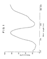
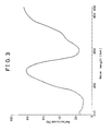
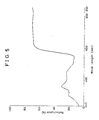
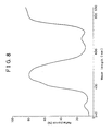
- Figs. 1 to 9 are graphs each illustrating the reflection peak of visible rays irradiated onto the aluminum substrate with thin film formed in Examples 1 to 9, respectively.
- In the process of the present invention, hydrophobic substance powder is applied as the material of thin films. The average particle diameter of said hydrophobic substance powder is preferably not more than 10 µm, particularly 1 to 0.01 µm. If the average particle diameter is in excess of 10 µm, there may be caused various disadvantages that it takes much time to disperse or dissolve in aqueous medium or it is difficult to disperse or dissolve homogeneously.
- The kind of said hydrophobic substance powder may be selected properly according to the uses of thin films to be formed, and various ones can be used irrespective of organic substance or inorganic substance. Examples of them are coloring matters for optical memory and organic coloring matters such as perylene, indigo, thioindigo, squalilium, dichlorobenzene, thiapyrylium, azo-type coloring matter, quinacridone, viologen, Sudan, lake pigment, phthalocyanine blue, photalocyanine green, anthracene, anthraquinone, phthalocyanine, metal complexes of phthalocyanine, derivatives thereof, porphyrin, metal complexes of porphyrin, and derivatives thereof; electrochromic materials such as 1,1′-diheptyl-4,4′-bipyridinium dibromide, 1,1′-didodecyl-4,4′-bipyridinium dibromide and the like, lightsensitive materials (photochromic materials) and light sensor materials such as 6-nitro-1,3,3-trimethylspiro-(2′H-1′-benzopyran-2,2′-indoline) (commonly called spiropyran) and the like; liquid crystal display coloring matters such as p-azoxyanisole and the like. Further examples are the hydrophobic compounds among the coloring matters each for electronics, recording, photo-chromism, photos, energy use, biomedicals, and coloring matters for food and cosmetics, dyes, coloring matters for specific coloring which are listed in "Color Chemical Cyclopedia", CMC Co., Ltd., pp542 - 717, March 28, 1988. Particularly preferred among the above are metal complexes and derivatives of phthalocyanine (Pc), specifically X-type and τ-type H₂-Pc, ε-type, Cu-Pc, VO-Pc, InCl-Pc, AlCl-Pc, α-type TiO-Pc, Mg-Pc and the like. Moreover, electrically conductive organic materials and gas sensor materials such as the 1:1 complex of 7,7,8,8-tetra-cyanoquinonedimethane (TCNQ) and tetrathiafulvalene (TTF), light curing paints such as pentaerythritol diacrylate and the like, diazo-type lightsensitive materials and paints such as 1-phenylazo-2-naphthol and the like can be used. Furthermore, water-insoluble polymers including general purpose polymers such as polycarbonate, polystyrene, polyethylene, polypropylene polyamide, polyphenylene sulfide (PPS), polyphenylene oxide (PPO), polyacrylonitrile (PAN) and the like; polyphenylene, polypyrrole, polyaniline, polythiophene, acetyl cellulose, poly(vinyl acetate), poly(vinyl butyral), and various polymers (poly(vinyl pyridine) and the like) and copolymers (copolymer of methyl methacrylate and methacrylic acid and the like) can be used.
- The inorganic hydrophobic substances therein may extend to those of various kinds in various manners, including TiO₂, C, CdS, WO₃, Fe₂O₃, Y₂O₃ ZrO₂ Al₂O₃, CuS, ZnS, TeO₂, LiNb₃O, Si₃N₄ and the like, and various kinds of superconductive oxides. Particularly by employing charge carrier generation materials (CGM) as said hydrophobic substance, preferable thin films as said photoconductor for electrophotography can be obtained.
- As the aqueous medium to be used in the present invention, various media such as water, mixture of water and alcohol, mixture of water and acetone, and the like can be used.
- On the other hand, surfactants used in the present invention are the surfactants having HLB value of 10.0 to 20.0, preferably 12 to 18. Preferred example of such surfactants are non-ionic surfactants such as polyoxyethylene alkylether, polyoxyethylene fatty acid ester, polyoxyethylene alkylphenylether, polyoxyethylene polyoxypropylene alkylether and the like. In addition, alkyl sulfates, polyoxyethylene alkylether sulfates, alkyltrimethylammonium chloride, fatty acid diethylaminoethyl amide and the like can also be used.
- As the surfactants, ferrocene derivatives can be also used. Said ferrocene derivatives include various kinds. Representative examples of them are ferrocene derivatives represented by the general formula:

- Further, Y indicates an oxygen (-O-) or an oxycarbonyl group (-C-O-), and R⁴ and R⁵ are each a hydrogen or a methyl group (CH₃). Accordingly,

- m indicates an integer of 1 to 18. Accordingly, between the ring member carbon atoms and the abovedescribed oxygen or an oxycarbonyl group, an alkylene group having 1 to 18 carbon atoms such as an ethylene group, a propylene group and the like is interposed. Further, in indicates the repeating number of abovedescribed oxyalkylene group including oxyethylene group and the like, and means not only integers but also real number including them in the rang eof 2.0 to 70.0, showing the mean value of the repeating number of oxyalkylene group and the like.
- In addition to the ferrocene derivatives represented by the above general formula (I), various ones including ammonium type and pyrridine type (International Patent Publication WO88/07538, etc.) can be used in the present invention. And further examples are the ferrocene derivatives described in the specifications of Japanese Patent Application Nos. 233797/1988, 233798/1988, 248600/1988, 248601/1988, 45370/1989, 54956/1989, 70680/1989, 70681/1989, 76498/1989 and 74699/1989.
- These ferrocene derivatives can very efficiently dissolve or disperse hydrophobic substances into aqueous medium.
- In the process of the present invention, one of the above surfactants and hydrophobic substance powder are added in an aqueous medium, and the mixture is stirred fully by the use of ultrasonic waves, homogenizer or stirrer for 1 hour to 7 days. By this operation, the hydrophobic substance powder is homogeneously dispersed or dissolved in the aqueous medium by the function of surfactant having a HLB value of 10.0 to 20.0, to be dispersion or aqueous solution.
- In the present invention, to the homogeneous dispersion or aqueous solution thus obtained, supporting salts are added if desired, or excessive hydrophobic substances are removed by centrifugation, decantation, static sedimentation or other ways according to the circumstances, and the resulting electrolyte is subjected to electrotreatment while allowing to stand or somewhat stirring. During the electrotreatment, hydrophobic substance powder may be supplementarily added to the electrolyte, or there may be provided a recycle circuit in which a part of electrolyte is withdrawn out of the system, the inorganic substance is added to the withdrawn electrolyte and thoroughly stirred, and then the resulting solution is returned to the system.
- The concentration of the surfactant in that process is not critical, but is usually selected in the range of 10 µM to 1 M, preferably 0.5 mM to 5 mM. In case various ferrocene derivatives (micelle forming agent) including ferrocene derivatives of abovedescribed general formula (I) are used as surfactant, the concentration of it should be the threshold micelle concentration or higher.
- The supporting salt is added, if necessary, in order to control the electrical conductance of the aqueous medium. The amount of the supporting salt added is not critical as long as it does not inhibit the deposition of the hydrophobic substance dissolved or dispersed in the solution, but usually about 0 to 300 times and preferably about 10 to 200 times that of the above surfactant. Said supporting salt is not necessarily inevitable to electrotreatment. without it, a film of high purity containing no supporting salt can be obtained. The type of supporting salt is not critical as long as it is able to control the electric conductance for the aqueous medium without inhibiting the dissolving or deposition of the above hydrophobic substance onto the electrode.
- Preferred examples of the supporting salts therein are specifically, sulfuric acid salts (salts of lithium, potassium, sodium, rubidium, aluminum and the like), acetic acid salts (salts of lithium, potassium, sodium, rubidium, beryllium, magnesium, calcium, strontium, barium, aluminum and the like), salts of halide (salts of lithium, potassium, sodium, rubidium, calcium, magnesium, aluminum and the like), salts of water soluble oxides (salts of lithium, potassium, sodium, rubidium, calcium, magnesium, aluminum and the like) which are generally and widely used as supporting salts.
- As the electrode, various ones can be used. Preferred examples of anodes are ITO (mixed oxide of indium oxide and tin oxide), platinum, gold, silver, glassy carbon, an electrically conductive metal oxide, an electrically conductive organic polymer and the like. Preferred examples of cathodes are base metals including aluminum, zinc, tin, iron, nickel, magnesium and the like, and alloys including stainless steel and the like. Besides the above, copper, platinum, gold, silver, glassy carbon, electrically conductive metal oxide, an electrically conductive organic polymer and the like, semiconductors such as crystalline silicone, amorphous silicone and the like can be applied. Particularly, it is preferred to use a metal more noble than the oxidation-reduction potential (against +0.15 to +0.30 V saturated calomel electrode) of ferrocene derivatives, or an electrically conductive substance. In case of producing photoconductor for electrophotography, aluminum, particularly aluminum substrate is used as the cathode.
- Conditions for electrotreatment in the present invention can be determined under the condition so that the thin film of abovementioned hydrophobic substance may be formed on the cathode. Therein the conditions that the thin film of said hydrophobic substance is formed on the cathode is not limited to the condition for forming hydrophobic thin film only, but include the condition for forming hydrophobic thin films on both the cathode and the anode. Such conditions vary with circumstances, specifically, electrotreatment is performed with a potentiostat or with a galvanostat at the liquid temperature of 0 to 100°C for the period of one minute to two hours. In the electrotreatment with potentiostat, the potential on the cathode should be controlled to -0.03 to -10.0 V and in the electrotreatment with a galvanostat, the current density should be controlled in the range of 1 µA/cm² to 100 mA/cm². Therein when the above ferrocene derivatives are used, the liquid temperature is 0 to 50°C, preferably 5 to 40°C, the potential of the cathode is -0.03 to -5.00 V, preferably -0.05 to -2.00 V. The current density should be 1 to 300 µA/cm², preferably 1 to 100 µA/cm². On the other hand, when surfactants other than ferrocene derivatives are used, the liquid temperature is room temperature to 100°C, the potential of the cathode is -0.5 to -10.0 V, and the current density is 50 µA/cm² to 100 mA/cm², preferably 100 µA/cm² to 10 mA/cm².
- On performing the electrotreatment in such conditions, environmental conditions of pH change drastically in the vicinity of the cathode, and as the result, the micelle becomes unstable, to separate and scatter. Accompanying with such a scattering of micelle, hydrophobic substances dissolved in the solution come to deposite on the cathode, to form uniform thin films tightly sticking to the cathode.
- The thin films obtained according to the process of the present invention are effectively subjected to, if necessary, post treatments such as electrowashing, solvent washing, and baking treatment at 100 to 300°C.
- Since films are formed on the cathode according to the present invention, thin films of hydrophobic substance can be formed on base metals including aluminum, which are applicable to photasensitive materials and the like.
- In addition, the process of the present invention can employ surfactants used generally has a very high value in practical use.
- The thin film formed according to the process of the present invention are extensively and effectively used as the materials for optical disk, optical memory, photosensitive material, color filters, solar battery, toner, pigments and the like.
- Particularly, the photoconductor for electrophotography obtained by carrying out the present invention with the use of aluminum substrate as the cathode, and charge carrier generation materials as hydrophobic substance are extensively and effectively used for photosensitive drums for copy, laser printer and the like.
- To produce a photoconductor for electrophotography according to the process of the present invention, charge carrier generation layer is formed on the cathode, as described before. On the formation of said charge carrier layer, it is effective to add an appropriate amount of binder polymer in the aqueous medium, if desired, to be included in the charge carrier generation layer to be formed, and heighten the mechanical strength of said layer. As the binder polymer to be used there, poly(vinyl butyral), poly(methyl methacrylate), polyester, poly(vinylidene chloride), polyamide, styrene-maleic anhydride polymer and the like can be used.
- Said photoconductor for electrophotography is formed fundamentally of base metals such as aluminum used as cathode and thin films of charge carrier generation layer formed on said base metal. If charge carrier transport layer (CTL) is formed on it further, still higher efficiency can be obtained. In forming said charge carrier transport layer, the process for producing thin films of the present invention may be employed or other processes (e.g., slip cast method, polymer binding method, deposition method and others) may be employed. As charge carrier transport material used for forming said charge carrier transport layer, compounds such as indoline, quinoline, triphenylamine, bisazo, pyrazole, pyrazoline, oxidiazole, thiazole, imidazole, hydrazone, triphenylmethane, carbazole, benzaldehyde and the like or derivatives thereof, and polymers or copolymers containing these compounds or printer and the like.
- To produce a photoconductor for electrophotography according to the process of the present invention, charge carrier generation layer is formed on the cathode, as described before. On the formation of said charge carrier layer, it is effective to add an appropriate amount of binder polymer in the aqueous medium, if desired, to be included in the charge carrier generation layer to be formed, and heighten the mechanical strength of said layer. As the binder polymer to be used there, poly(vinyl butyral), poly(methyl methacrylate), polyester, poly(vinylidene chloride), polyamide, styrene-maleic anhydride polymer and the like can be used.
- Said photoconductor for electrophotography is formed fundamentally of base metals such as aluminum used as cathode and thin films of charge carrier generation layer formed on said base metal. If charge carrier transport layer (CTL) is formed on it further, still higher efficiency can be obtained. In forming said charge carrier transport layer, the process for producing thin films of the present invention may be employed or other processes (e.g., slip cast method, polymer binding method, deposition method and others) may be employed. As charge carrier transport material used for forming said charge carrier transport layer, compounds such as indoline, quinoline, triphenylamine, bisazo, pyrazole, pyrazoline, oxidiazole, thiazole, imidazole, hydrazone, triphenylmethane, carbazole, benzaldehyde and the like or derivatives thereof, and polymers or copolymers containing these compounds or derivatives as substituents, or blends of the above compounds or derivatives and various polymer or copolymers.
- Then, the present invention is described in greater detail with reference to the examples and the comparative examples.
- To 100 ml of water was added surfactant shown in Table 1 so that the concentration might become 2 mmol/L (L=liter) to obtain the solution. Then, to the solution was added hydrophobic powder having the specified average particle diameter to make 10 mM and the resulting mixture was stirred by ultrasonic wave for 10 minutes at 25°C, followed by stirring with a magnetic stirrer for 3 days.
- The solution thus obtained was diluted to 1/25 in concentration and visible absorbance was measured to calculate the solubility from the value. The results are shown in Table 1. From the Table, it can be seen that hydrophobic powder is sufficiently soluble (dispersed) in water.
- Subsequently, an electrolyte was prepared by adding lithium bromide to the above pre-diluted solution (dispersion) to make 0.1 mol/L. By using this electrolyte, as well as by using aluminum or platinum as the reaction electrode (cathode), a platinum electrode as the opposite electrode (anode), applying the voltage at 25°C, controlled electric current electrolysis was carried out for 15 minutes so that an electric current density should become 0.2 mA/cm².
- As the result, a thin film was formed on the aluminum (or platinum) substrate. On the aluminum (or platinum) substrate, on which this thin film was formed, visible ray was irradiated and the reflection peak was measured. The results were shown in Fig. 1 to 9 corresponding to Example 1 to 9, respectively).
- The reflection peak confirmed that the thin film on the aluminum (or platinum) substrate was made of phthalocyanine.
- Further, a hydrophobic thin film could be formed by connecting the reference electrode (a saturated calomel electrode) to the above electrolyte, adjusting the potential of reaction electrode to 1.5 to 2.0 V lower than the reference electrode and passing the electricity (controlled potential electrolysis).
Table 1 NO. Surfactant HLB-value Solubility*9 (mM) Hydrophobic Material Cathode Electric Current Density (mA/cm²) Reflection Spectrum Example 1 Brij 35*1 10 or more 4.2 Phthalocyanine (0.22 µm) Aluminum 0.2 Fig. 1 Example 2 Brij 35 10 or more 4.2 Phthalocyanine (0.22 µm) Platinum 0.1 Fig. 2 Example 3 Brij 35 10 or more 4.2 Phthalocyanine (0.22 µm) Aluminum 0.1 Fig. 3 Example 4 BL-25*2 19.5 5.4 Paliogen Red K3580 (0.07 µm) Aluminum 0.1 Fig. 4 Example 5 BC-23*3 18.0 5.2 Lithol Scarlet K3700 (0.08 µm) Aluminum 0.1 Fig. 5 Example 6 NP-10*4 18.0 5.6 Tetraphenylporphyrin (0.26 µm) Aluminum 0.1 Fig. 6 Example 7 MYL-10*5 12.5 1.5 Heliogen Blue K6902 (0.12 µm) Aluminum 0.1 Fig. 7 Example 8 Brij 35 10 or more 4.2 Copper phthalocyanine (0.19 µm) Aluminum 0.5 Fig. 8 Example 9 TAMNS-10*6 10.0 4.9 Phthalocyanine (0.18 µm) Aluminum 0.8 Fig. 9 Comparative Example 1 MYS-4*7 6.5 0 Phthalocyanine (0.22 µm) Aluminum Film not formed - Comparative Example 2 NP-2*8 4.5 0 Phthalocyanine (0.22 µm) Aluminum Film not formed - *1 Kao Co., Ltd. *2 Nikko Chemical Co., Ltd. Polyoxyethylenelaurylether *3 Nikko Chemical Co., Ltd. Polyoxyethylenecetylether *4 Nikko Chemical Co., Ltd. Polyoxyethylenenonylphenylether *5 Nikko Chemical Co., Ltd. Polyosyethylenemonolaurate *6 Nikko Chemical Co., Ltd. Polyoxyethylenestearylamine *7 Nikko Chemical Co., Ltd. Polyethyleneglycolmonostearate *8 Nikko Chemical Co., Ltd. Polyethylenenonylphenylether *9 Shown as the concentration of hydrophobic material solution in 2 mM surfactant - To 100 ml of water was added nonionic surfactant (produced by Nikko Chemical Co., Ltd. polyoxyethylenenonylphenylether, HLB-value=18) so that the concentration might become 2 mmol/L to obtain the solution. Then, to the solution was added phthalocyanine (produced by Tokyo Kasei Co., Ltd.) having an average particule diameter of 0.22 µm (Examples 10 to 12) or copper phthalocyanine (produced by Tokyo Kasei Co., Ltd.) having an average particle diameter of 0.19 µm (Example 13) to make 10 mM and the resulting mixture was stirred by ultrasonic wave for 10 minutes at 25°C, followed by stirring with a magnetic stirrer for 3 days.
- Then, the electrolyte was prepared by adding lithium bromide to the solution to make 0.1 mol/L. By using this electrolyte, as well as by using aluminum electrode as the reaction electrode (cathode) and ITO electrode as the opposite electrode (anode), applying the voltage at 25°C, controlled electric current electrolysis was carried out so that the electric current density might become 0.1 to 0.2 mA/cm².
- As the result, a thin film of phthalocyanine (Examples 10 to 12) or a thin film of copper phthalocyanine (Example 13) was formed on the aluminum substrate as the cathode.
- The thin film of phthalocyanine or the thin film of copper phthalocyanine (charge carrier generation layer; CGL) was sufficiently washed with ethanol, dried and subjected to spincoating with chlorobenzene solution (concentration, 11 wt%) of polyvinylcarbazole to form charge carrier transport layer (CTL) having a thickness of 6 to 8 µm. Thus, photoconductor was obtained containing CTL of polyvinylcarbazole, CGL of phthalocyanine (or copper phthalocyanine) and aluminum electrode.
- Further, the performance of the photoconductor was evaluated, using a test machine of SP428 type (manufactured by Kawaguchi Electric Co., Ltd.) as following. That is, the above photoconductor was subjected to corona charge at -7.0 kV for 30 seconds and the surface of the photoconductor was charged negative.
- Let the surface potential be Vd, and light with wavelength of 610 nm or 630 nm was irradiated (output: 1 µW), and the period (second) in which the potential become half (1/2 Vd) was found. The luminous energy in that period (intensity of light x period, Unit: µJ/cm²) was let to be the indication of the ability of photoconductor to light with wavelength of 610 nm or 630 nm. The results are shown in Table 2.
- The photoconductor was prepared in the same manner as in Example 10 except that a thin film of phthalocyanine as CGL was formed by the vacuum deposition method. The performance was evaluated in the same manner. The results are shown in Table 2.
Table 2 Preparation Condition of CGL No. Electrolysis Mode Electric Current Density (mA/cm²) Amount of Electric Current (C/cm²) Material of CGL Material of CTL Vd (V) Photosensitivity (exposure required for half decay of charge voltage) (µJ/cm²) Example 10 Constant Current 0.2 0.13 Phthalocyanine Polyvinylcarbazole -540 72 Example 11 Constant Current 0.1 0.13 Phthalocyanine Polyvinylcarbazole -490 60 Example 12 Constant Current 0.1 0.13 Phthalocyanine* Polyvinylcarbazole -500 40 Example 13 Constant Current 0.2 0.13 Copper Phthalocyanine Polyvinylcarbazole -470 60 Comparative Example 3 - - - Phthalocyanine Polyvinylcarbazole -460 200 * CGL was washed with chloronaphthalene. - To 100 cc of water was added micelle forming agent of ferrocene derivative represented by the structural formula 1 to make 2 mM solution. To 20 cc of micelle solution was added 0.1 g of phthalocyanine and the resulting mixture was stirred by ultrasonic wave for 10 minutes to disperse and dissolve. After stirring with a stirrer 2 days and nights, obtained dispersed and dissolved micelle solution was subjected to centrifugal separation for 30 minutes at 2000 rpm. A visible absorption spectrum of the supernatant confirmed that phthalocyanine was dispersed.
- To the dispersed and dissolved micelle solution was added lithium bromide to make 0.1 M and was stirred with a stirrer for 10 minutes. By using this solution as an electrolyte, as well as by using platinum plate as the anode, ITO glass electrode as the cathode and a saturated calomel electrode as the reference electrode, controlled potential electrolysis was carried out at 25°C, at the applied voltage of -0.5 V, with an electric current density of 11.0 µA/cm² for 30 minutes. The amount of electric current was 0.02 coulomb (C).
- As the result, a thin film of phthalocyanine was obtained on the ITO transparent glass electrode. Since the absorption spectrum of phthalocyanine on the ITO transparent glass electrode agreed with that of the dispersed and soluble micelle solution, it can be seen that the thin film on the ITO transparent glass electrode was phthalocyanine and the thickness of the film was 0.6 µm from the absorbance.

- To 100 cc of water was added micelle forming agent of ferrocene derivative represented by the structural formula 2 to make 2 mM. To 20 cc of micelle solution was added 0.1 g of perylene-based pigment (K3580) (produced by BASF Co., Ltd.) and the resulting mixture was stirred by ultrasonic wave for 10 minutes to disperse and dissolve. After stirring with a stirrer 2 days and nights, obtained dispersed and soluble micelle solution was subjected to centrifugal separation for 30 minutes at 2000 rpm. A visible absorption spectrum of the supernatant confirmed that K3580 was dispersed.
- To the dispersed and dissolved micelle solution was added lithium bromide to make 0.1 M and was stirred with a stirrer for 10 minutes. By using this solution as an electrolyte, as well as by using a platinum plate as the anode, aluminum electrode as the cathode and a saturated calomel electrode as the reference electrode, controlled potential electrolysis was carried out at 25°C, at the applied voltage of -0.8 V, with an electric current density of 22.0 µA/cm² for 30 minutes. The amount of electric current was 0.03 C.
- As the result, a thin film of K3580 was obtained on the aluminum electrode. Since the peak wavelength of reflection spectrum of Ke3580 on the aluminum electrode agreed with that of absorption spectrum of the dispersed and soluble micelle solution, it can be seen that the thin film on the aluminum electrode was K3580 and an electron microtomograph showed the thickness of the film was 0.4 µm.

- To 100 cc of water was added micelle forming agent of ferrocene derivative represented by the structural formula 3 to make 2 mM. To 20 cc of micelle solution was added 0.1 g of copper phthalocyanine (produced by Dainichi Seika Co., Ltd.) and the resulting mixture was stirred by ultrasonic wave for 10 minutes to disperse and dissolve. After stirring with a stirrer 2 days and nights, obtained dispersed and soluble micelle solution was subjected to centrifugal separation for 30 minutes at 2000 rpm. A visible absorption spectrum of the supernatant confirmed that copper phthalocyanine was dispersed.
- To the dispersed and dissolved micelle solution was added lithium bromide to make 0.1 M and was stirred with a stirrer for 10 minutes. By using this solution as an electrolyte, as well as by using a platinum plate as the anode, aluminum electrode as the cathode and a saturated calomel electrode as the reference electrode, controlled potential electrolysis was carried out at 25°C, at the applied voltage of -0.3 V, with an electric current density of 7.6 µA/cm² for 30 minutes. The amount of electric current was 0.015 C.
- As the result, a thin film of copper phthalocyanine was obtained on the aluminum electrode. Since the peak wavelength of reflection spectrum of copper phthalocyanine on the aluminum electrode agreed with that of the absorption spectrum of the dispersed and soluble micelle solution, it can be seen that the thin film on the aluminum electrode was copper phthalocyanine and an electron microtomograph showed the thickness of the film was 0.25 µm.

- To 100 cc of water was added micelle forming agent of ferrocene derivative represented by the structural formula 4 to make 2 mM. To 20 cc of micelle solution was added 0.1 g of viologen and the resulting mixture was stirred by ultrasonic wave for 10 minutes to disperse and dissolve. After stirring with a stirrer 2 days and nights, obtained dispersed and soluble micelle solution was subjected to centrifugal separation for 30 minutes at 2000 rpm. A visible absorption spectrum of the supernatant confirmed that viologen was dispersed.
- To the dispersed and dissolved micelle solution was added lithium bromide to make 0.1 M and was stirred with a stirrer for 10 minutes. By using this solution as an electrolyte, as well as by using a platinum plate as the anode, copper electrode as the cathode and a saturated calomel electrode as the reference electrode, controlled potential electrolysis was carried out at 25°C, at the applied voltage of -0.7 V, with an electric current density of 17.6 µA/cm² for 30 minutes. The amount of electric current was 0.03 C.
- As the result, a thin film of viologen was obtained on the copper electrode. Since the peak wavelength of reflection spectrum of viologen on the copper electrode agreed with that of the absorption spectrum of the dispersed and soluble micelle solution, it can be seen that the thin film on the copper electrode was viologen an electron microtomograph showed and the thickness of the film was 0.65 µm.

- To 100 cc of water was added micelle forming agent of ferrocene derivative represented by the structural formula 5 to make 2 mM. To 20 cc of micelle solution was added 0.1 g of CuPcCl₈Br₈ (L9361) (produced by BASF Co., Ltd.) and the resulting mixture was stirred by ultrasonic wave for 10 minutes to disperse and dissolve. After stirring with a stirrer 2 days and nights, obtained dispersed and soluble micelle solution was subjected to centrifugal separation for 30 minutes at 2000 rpm. A visible absorption spectrum of the supernatant confirmed that L9361 was dispersed.
- To the dispersed and dissolved micelle solution was added lithium bromide to make 0.1 M and was stirred with a stirrer for 10 minutes. By using this solution as an electrolyte, as well as by using a platinum plate as the anode, polyaniline/ITO electrode as the cathode and a saturated calomel electrode as the reference electrode, controlled potential electrolysis was carried out at 25°C, at the applied voltage of -0.7 V, with an electric current density of 11.3 µA/cm² for 30 minutes. The amount of electric current was 0.02 C.
- As the result, a thin film of L9361 was obtained on the polyaniline/ITO electrode. Since the peak wavelength of the reflection spectrum of L9361 on the polyaniline/ITO electrode agreed with that of the absorption spectrum of the dispersed and soluble micelle solution, it can be seen that the thin film on the polyaniline/ITO electrode was L9361 and an electron microtomograph showed the thickness of the film was 0.6 µm.

- To 100 cc of water was added micelle forming agent of ferrocene derivative represented by the structural formula 6 to make 2 mM. To 20 cc of the micelle solution was added 0.1 g of Sudan I and the resulting mixture was stirred by ultrasonic wave for 10 minutes to disperse and dissolve. After stirring with a stirrer 2 days and nights, dispersed and dissolved micelle solution obtained was subjected to centrifugal separation for 30 minutes at 2000 rpm. A visible absorption spectrum of the supernatant confirmed that Sudan I was dispersed.
- To the dispersed and soluble micelle solution was added lithium bromide to make 0.1 M and was stirred with a stirrer for 10 minutes. By using this solution as an electrolyte, as well as by using a platinum plate as the anode, stainless electrode as the cathode and a saturated calomel electrode as the reference electrode, controlled potential electrolysis was carried out at 25°C, at the applied voltage of -0.5 V, with an electric current density of 8.6 µA/cm² for 30 minutes. The amount of electric current was 0.01 C.
- As the result, a thin film of Sudan I was obtained on the stainless electrode. Since the peak wavelength of the reflection spectrum of Sudan I on the stainless electrode agreed with that of the absorption spectrum of the dispersing and dissolving micelle solution, it can be seen that the thin film on the stainless electrode was Sudan I and an electron microtomograph showed the thickness of the film was 0.2 µm.

- To 100 cc of water was added micelle forming agent of ferrocene derivative represented by the structural formula 7 to make 2 mM. To 20 cc of micelle solution was added 0.1 g of tetraphenylporphyrin zinc complex (Zn-TPP) and the resulting mixture was stirred by ultrasonic wave for 10 minutes to disperse and dissolve. After stirring with a stirrer 2 days and nights, dispersing and dissolving micelle solution obtained was subjected to centrifugal separation for 30 minutes at 2000 rpm. A visible absorption spectrum of the supernatant confirmed that Zn-TPP was dispersed.
- To the dispersed and dissolved micelle solution was added lithium bromide to make 0.1 M and was stirred with a stirrer for 10 minutes. By using this solution as an electrolyte, as well as by using a platinum plate as the anode, platinum electrode as the cathode and a saturated calomel electrode as the reference electrode, controlled potential electrolysis was carried out at 25°C, at the applied voltage of -0.6 V, with an electric current density of 17.2 µA/cm² for 30 minutes. The amount of electric current was 0.03 C.
- As the result, a thin film of Zn-TPP was obtained on the platinum electrode. Since the peak wavelength of the reflection spectrum of Zn-TPP on the platinum electrode agreed with that of the absorption spectrum of the dispersed and dissolved micelle solution, it can be seen that the thin film on the platinum electrode was Zn-TPP and an electron microtomograph showed the thickness of the film was 0.18 µm.

- To 100 cc of water was added micelle forming agent of ferrocene derivative represented by the structural formula 8 to make 2 mM. To 20 cc of micelle solution was added 0.1 g of triphenylamine and the resulting mixture was stirred by ultrasonic wave for 10 minutes to disperse and dissolve. After stirring with a stirrer 2 days and nights, obtained dispersed and soluble micelle solution was subjected to centrifugal separation for 30 minutes at 2000 rpm. A visible absorption spectrum of the supernatant confirmed that triphenylamine was dispersed.
- To the dispersed and soluble micelle solution was added lithium bromide to make 0.1 M and was stirred with a stirrer for 10 minutes. By using this solution as an electrolyte, as well as by using a platinum plate as the anode, aluminum electrode as the cathode and a saturated calomel electrode as the reference electrode, controlled potential electrolysis was carried out at 25°C, at the applied voltage of -0.9 V, with an electric current density of 25.3 µA/cm² for 30 minutes. The amount of electric current was 0.04 C.
- As the result, a thin film of triphenylamine was obtained on the aluminum electrode. Since the peak wavelength of the reflection spectrum of triphenylamine on the aluminum electrode agreed with that of the absorption spectrum of the dispersed and soluble micelle solution, it can be seen that the thin film on the aluminum electrode was triphenylamine and an electron microtomograph showed the thickness of the film was 0.45 µm.

- To 100 cc of water was added micelle forming agent of ferrocene derivative represented by the structural formula 9 to make 2 mM. To 20 cc of micelle solution was added 0.1 g of lake pigment (K3700) (BASF Co., Ltd.) and the resulting mixture was stirred by ultrasonic wave for 10 minutes to disperse and dissolve. After stirring with a stirrer 2 days and nights, obtained dispersed and soluble micelle solution was subjected to centrifugal separation for 30 minutes at 2000 rpm. A visible absorption spectrum of the supernatant confirmed that K3700 was dispersed.
- To the dispersed and dissolved micelle solution was added lithium bromide to make 0.1 M and was stirred with a stirrer for 10 minutes. By using this solution as an electrolyte, as well as by using a platinum plate as the anode, glassycarbon (GC) electrode as the cathode and a saturated calomel electrode as the reference electrode, controlled potential electrolysis was carried out at 25°C, at the applied voltage of -0.8 V, with an electric current density of 12.8 µA/cm² for 30 minutes. The amount of electric current was 0.25 C.
- As the result, a thin film of K3700 was obtained on the GC electrode. Since the peak wavelength of the reflection spectrum of K3700 on the GC electrode agreed with that of the absorption spectrum of the dispersed and soluble micelle solution, it can be seen that the thin film on the GC electrode was K3700 and an electron microtomograph showed the thickness of the film was 0.4 µm.

- To 100 cc of water was added micelle forming agent of ferrocene derivative represented by the structural formula 10 to make 2 mM. To 20 cc of micelle solution was added 0.1 g of naphthol AS and the resulting mixture was stirred by ultrasonic wave for 10 minutes to disperse and dissolve. After stirring with a stirrer 2 days and nights, dispersed and dissolved micelle solution obtained was subjected to centrifugal separation for 30 minutes at 2000 rpm. A visible absorption spectrum of the supernatant confirmed that naphthol AS was dispersed.
- To the dispersed and soluble micelle solution was added lithium bromide to make 0.1 M and was stirred with a stirrer for 10 minutes. By using this solution as an electrolyte, as well as by using a platinum plate as the anode, ITO glass electrode as the cathode and a saturated calomel electrode as the reference electrode, controlled potential electrolysis was carried out at 25°C, at the applied voltage of -0.5 V, with an electric current density of 5.5 µA/cm² for 30 minutes. The amount of electric current was 0.01 C.
- As the result, a thin film of naphthol AS was obtained on the ITO glass electrode. Since the peak wavelength of the absorption spectrum of naphthol AS on the ITO glass electrode agreed with that of the absorption of the dispersed and dissolved micelle solution, it can be seen that the thin film on the ITO glass electrode was naphthol AS and an electron microtomograph showed the thickness of the film was 0.4 µm.

Claims (12)
Applications Claiming Priority (6)
| Application Number | Priority Date | Filing Date | Title |
|---|---|---|---|
| JP317627/88 | 1988-12-17 | ||
| JP63317626A JPH0759757B2 (en) | 1988-12-17 | 1988-12-17 | Thin film manufacturing method |
| JP31762788A JPH02163745A (en) | 1988-12-17 | 1988-12-17 | Production of electrophotographic photosensitive body |
| JP317626/88 | 1988-12-17 | ||
| JP11748189A JPH02298294A (en) | 1989-05-12 | 1989-05-12 | Production of thin film |
| JP117481/88 | 1989-05-12 |
Publications (2)
| Publication Number | Publication Date |
|---|---|
| EP0374643A2 true EP0374643A2 (en) | 1990-06-27 |
| EP0374643A3 EP0374643A3 (en) | 1991-07-17 |
Family
ID=27313385
Family Applications (1)
| Application Number | Title | Priority Date | Filing Date |
|---|---|---|---|
| EP19890122737 Withdrawn EP0374643A3 (en) | 1988-12-17 | 1989-12-09 | Process for producing thin films |
Country Status (3)
| Country | Link |
|---|---|
| US (1) | US5122247A (en) |
| EP (1) | EP0374643A3 (en) |
| CA (1) | CA2004789A1 (en) |
Cited By (2)
| Publication number | Priority date | Publication date | Assignee | Title |
|---|---|---|---|---|
| EP0440095A2 (en) * | 1990-01-30 | 1991-08-07 | Idemitsu Kosan Company Limited | Process for producing thin films and color filters |
| CN110358515A (en) * | 2019-06-13 | 2019-10-22 | 中国石油化工股份有限公司 | Oil well inhibition composition and preparation method thereof, Inhibitor For Oil Well System |
Families Citing this family (11)
| Publication number | Priority date | Publication date | Assignee | Title |
|---|---|---|---|---|
| US5240797A (en) * | 1988-04-30 | 1993-08-31 | Seiko Epson Corporation | Thin film device and method of manufacture |
| JP2774351B2 (en) * | 1990-03-26 | 1998-07-09 | 出光興産株式会社 | Organic thin-film electroluminescence device and method of manufacturing the same |
| JP2949392B2 (en) * | 1992-09-07 | 1999-09-13 | 日石三菱株式会社 | Manufacturing method of color filter |
| WO1999000536A2 (en) * | 1997-06-27 | 1999-01-07 | University Of Southampton | Porous film and method of preparation thereof |
| US6127192A (en) * | 1998-08-27 | 2000-10-03 | Micron Technology, Inc. | Complexes having tris (pyrazolyl) borate ligands for forming films |
| US6683175B2 (en) * | 2001-04-12 | 2004-01-27 | Canon Kabushiki Kaisha | Porphyrin compound, and electrophotographic photosensitive member, process-cartridge and apparatus using the compound |
| US20050004336A1 (en) * | 2003-05-08 | 2005-01-06 | Mabrouk Patricia Ann | Method for synthesizing conducting polymers from neat monomer solutions |
| WO2011109020A1 (en) * | 2010-03-03 | 2011-09-09 | Alliance For Sustainable Energy, Llc | Electrochemical nitridation of metal surfaces |
| DE102016215709A1 (en) * | 2015-08-28 | 2017-03-02 | Tsubakimoto Chain Co. | Chain component and chain |
| CN113308111A (en) * | 2021-06-03 | 2021-08-27 | 宁夏清研高分子新材料有限公司 | Liquid crystal polymer film for flexible printed circuit board and preparation method thereof |
| CN117510758B (en) * | 2024-01-05 | 2024-04-02 | 淄博鲁华泓锦新材料集团股份有限公司 | Styrene-isoprene-styrene continuous hydrogenation process based on tubular reaction |
Citations (1)
| Publication number | Priority date | Publication date | Assignee | Title |
|---|---|---|---|---|
| WO1988007538A1 (en) * | 1987-03-31 | 1988-10-06 | Idemitsu Kosan Company Limited | Ferrocene derivatives and process for preparing thin organic film |
Family Cites Families (12)
| Publication number | Priority date | Publication date | Assignee | Title |
|---|---|---|---|---|
| US3971708A (en) * | 1971-07-08 | 1976-07-27 | Scm Corporation | Electrocoating process |
| CA1083756A (en) * | 1975-08-07 | 1980-08-19 | George P. Koch | Prevention of water staining of aluminum |
| US4343885A (en) * | 1978-05-09 | 1982-08-10 | Dynachem Corporation | Phototropic photosensitive compositions containing fluoran colorformer |
| JPS56152765A (en) * | 1980-04-30 | 1981-11-26 | Kansai Paint Co Ltd | Formation of olefin resin coating film |
| GB2130218B (en) * | 1982-11-18 | 1986-06-18 | Ici Plc | Electrodepositable coating compositions |
| JPS60179702A (en) * | 1984-02-28 | 1985-09-13 | Seiko Instr & Electronics Ltd | Manufacture of colored body with multicolored surface |
| GB8411890D0 (en) * | 1984-05-10 | 1984-06-13 | Albright & Wilson | Dyeing processes |
| US4839322A (en) * | 1986-05-05 | 1989-06-13 | The Lubrizol Corporation | High surface area polymers of pyrrole or copolymers of pyrrole |
| JPS63243298A (en) * | 1987-03-31 | 1988-10-11 | Idemitsu Kosan Co Ltd | Production of organic thin film |
| DE3852818T2 (en) * | 1987-08-28 | 1995-05-24 | Idemitsu Kosan Co | FERROCENER DERIVATIVES, SURFACE ACTIVE AGENTS THAT CONTAIN THEM AND METHOD FOR PRODUCING THIN ORGANIC FILMS. |
| US5015748A (en) * | 1988-10-01 | 1991-05-14 | Idemitsu Kosan Co., Ltd. | Novel ferrocene derivatives, surfactants containing same and a process for producing organic thin films |
| JPH02250892A (en) * | 1989-03-24 | 1990-10-08 | Idemitsu Kosan Co Ltd | New ferrocene derivative, surfactant containing the same and production of organic thin film |
-
1989
- 1989-12-01 US US07/444,817 patent/US5122247A/en not_active Expired - Fee Related
- 1989-12-06 CA CA002004789A patent/CA2004789A1/en not_active Abandoned
- 1989-12-09 EP EP19890122737 patent/EP0374643A3/en not_active Withdrawn
Patent Citations (1)
| Publication number | Priority date | Publication date | Assignee | Title |
|---|---|---|---|---|
| WO1988007538A1 (en) * | 1987-03-31 | 1988-10-06 | Idemitsu Kosan Company Limited | Ferrocene derivatives and process for preparing thin organic film |
Non-Patent Citations (2)
| Title |
|---|
| CHEMISTRY LETTERS, no. 4, April 1988, pages 693-696, The Chemical Society of Japan; T. SAJI: "Electrochemical formation of a phthalocyanine thin film by disruption of micellar aggregates" * |
| J. AM. CHEM. SOC., vol. 109, 1987, pages 5881-5883, American Chemical Society; K. HOSHINO et al.: "Electrochemical formation of an organic thin film by disruption of micelles" * |
Cited By (3)
| Publication number | Priority date | Publication date | Assignee | Title |
|---|---|---|---|---|
| EP0440095A2 (en) * | 1990-01-30 | 1991-08-07 | Idemitsu Kosan Company Limited | Process for producing thin films and color filters |
| EP0440095A3 (en) * | 1990-01-30 | 1992-06-10 | Idemitsu Kosan Company Limited | Process for producing thin films and color filters |
| CN110358515A (en) * | 2019-06-13 | 2019-10-22 | 中国石油化工股份有限公司 | Oil well inhibition composition and preparation method thereof, Inhibitor For Oil Well System |
Also Published As
| Publication number | Publication date |
|---|---|
| CA2004789A1 (en) | 1990-06-17 |
| EP0374643A3 (en) | 1991-07-17 |
| US5122247A (en) | 1992-06-16 |
Similar Documents
| Publication | Publication Date | Title |
|---|---|---|
| US5203974A (en) | Process for producing thin films | |
| EP0374643A2 (en) | Process for producing thin films | |
| US5128226A (en) | Electrophotographic element containing barrier layer | |
| EP0340968A2 (en) | Thin film device and method of manufacturing the same | |
| US5041582A (en) | Novel ferrocene derivatives, surfactants containing same and process for producing organic thin films | |
| Umeda et al. | Energy gap dependence of the photocarrier generation efficiency in layered organic photoreceptors | |
| JPH0762594A (en) | Thin film, its production and functional element using the thin film | |
| US5232800A (en) | Method for improving charge mobility in electrophotographic photoreceptors | |
| JPH05333575A (en) | Electrophotographic sensitive body | |
| EP0331745B1 (en) | Ferrocene derivatives, surfactants containing same, and process for producing thin organic film | |
| EP0402980A1 (en) | Electrophotographic recording material | |
| JP2885467B2 (en) | Method for producing thin film and electrophotographic photoreceptor | |
| US5028504A (en) | Infrared-sensitive photoconductor elements incorporating a cyanine dye and a perylene pigment | |
| JP2738457B2 (en) | Thin film manufacturing method | |
| US3560208A (en) | Cyanine dye containing a pyrrole nucleus used as a sensitizer for organic photoconductors | |
| JP2557834B2 (en) | Electrophotographic photoreceptor | |
| US4025342A (en) | Organic semiconductors used in photoconductor element | |
| JP2800224B2 (en) | Electrophotographic photoreceptor | |
| JPH0430172A (en) | Manufacture of thin film and electrophotographic sensitive body | |
| US5248579A (en) | Electrophotographic recording material | |
| JPH068516B2 (en) | Thin film manufacturing method | |
| JPH02164435A (en) | Production of thin membrane | |
| JPH0323458A (en) | Manufacture of electrophotographic sensitive body | |
| Biswas et al. | Recent advances in photoconductive and photosensitive polymers | |
| JPH0826476B2 (en) | Organic thin film manufacturing method |
Legal Events
| Date | Code | Title | Description |
|---|---|---|---|
| PUAI | Public reference made under article 153(3) epc to a published international application that has entered the european phase |
Free format text: ORIGINAL CODE: 0009012 |
|
| AK | Designated contracting states |
Kind code of ref document: A2 Designated state(s): BE CH DE FR GB IT LI NL SE |
|
| 17P | Request for examination filed |
Effective date: 19901220 |
|
| PUAL | Search report despatched |
Free format text: ORIGINAL CODE: 0009013 |
|
| AK | Designated contracting states |
Kind code of ref document: A3 Designated state(s): BE CH DE FR GB IT LI NL SE |
|
| 17Q | First examination report despatched |
Effective date: 19921102 |
|
| STAA | Information on the status of an ep patent application or granted ep patent |
Free format text: STATUS: THE APPLICATION IS DEEMED TO BE WITHDRAWN |
|
| 18D | Application deemed to be withdrawn |
Effective date: 19931208 |