EP0373607A2 - Focusing error detection circuit - Google Patents
Focusing error detection circuit Download PDFInfo
- Publication number
- EP0373607A2 EP0373607A2 EP89122962A EP89122962A EP0373607A2 EP 0373607 A2 EP0373607 A2 EP 0373607A2 EP 89122962 A EP89122962 A EP 89122962A EP 89122962 A EP89122962 A EP 89122962A EP 0373607 A2 EP0373607 A2 EP 0373607A2
- Authority
- EP
- European Patent Office
- Prior art keywords
- focusing error
- focusing
- sample
- detection circuit
- signal
- Prior art date
- Legal status (The legal status is an assumption and is not a legal conclusion. Google has not performed a legal analysis and makes no representation as to the accuracy of the status listed.)
- Granted
Links
Images

Classifications
-
- G—PHYSICS
- G11—INFORMATION STORAGE
- G11B—INFORMATION STORAGE BASED ON RELATIVE MOVEMENT BETWEEN RECORD CARRIER AND TRANSDUCER
- G11B7/00—Recording or reproducing by optical means, e.g. recording using a thermal beam of optical radiation by modifying optical properties or the physical structure, reproducing using an optical beam at lower power by sensing optical properties; Record carriers therefor
- G11B7/08—Disposition or mounting of heads or light sources relatively to record carriers
- G11B7/09—Disposition or mounting of heads or light sources relatively to record carriers with provision for moving the light beam or focus plane for the purpose of maintaining alignment of the light beam relative to the record carrier during transducing operation, e.g. to compensate for surface irregularities of the latter or for track following
- G11B7/094—Methods and circuits for servo offset compensation
-
- G—PHYSICS
- G11—INFORMATION STORAGE
- G11B—INFORMATION STORAGE BASED ON RELATIVE MOVEMENT BETWEEN RECORD CARRIER AND TRANSDUCER
- G11B7/00—Recording or reproducing by optical means, e.g. recording using a thermal beam of optical radiation by modifying optical properties or the physical structure, reproducing using an optical beam at lower power by sensing optical properties; Record carriers therefor
- G11B7/08—Disposition or mounting of heads or light sources relatively to record carriers
- G11B7/09—Disposition or mounting of heads or light sources relatively to record carriers with provision for moving the light beam or focus plane for the purpose of maintaining alignment of the light beam relative to the record carrier during transducing operation, e.g. to compensate for surface irregularities of the latter or for track following
- G11B7/0908—Disposition or mounting of heads or light sources relatively to record carriers with provision for moving the light beam or focus plane for the purpose of maintaining alignment of the light beam relative to the record carrier during transducing operation, e.g. to compensate for surface irregularities of the latter or for track following for focusing only
- G11B7/0909—Disposition or mounting of heads or light sources relatively to record carriers with provision for moving the light beam or focus plane for the purpose of maintaining alignment of the light beam relative to the record carrier during transducing operation, e.g. to compensate for surface irregularities of the latter or for track following for focusing only by astigmatic methods
Definitions
- This invention relates to a focusing error detection circuit which may be employed conveniently with, for example, an optical pickup of an optical disk apparatus.
- an optical pickup device In a conventional apparatus for recording and/or reproducing information signals on or from an optical disk, an optical pickup device is employed, in which a light beam from a semiconductor laser collected by an object lens is irradiated on the recording tracks of an optical disk and the reflected return light from the disk is detected to effect readout and/or writing of the information signals.
- Such optical pickup device includes a built-in focusing control unit for controlling an object lens so that the light beam collected by the object lens is irradiated on the recording tracks of the optical lens in the focused state.
- focusing control unit performs focusing control by driving a supporting unit, which movably supports the object lens in two directions, that is, along the optical axis of the object lens and along the direction normal to the optical axis and within a horizontal plane, on the basis of the focusing error signals.
- the supporting unit for supporting the object lens in the two mutually perpendicular directions is shown for example in the US Patent 4473274.
- the focusing error signals are produced by detecting at a photodetector the state of the reflected return light which is once irradiated on and reflected by the disk surface.
- a focusing error detection circuit operating in accordance with the astigmatic method such as a disclosed in the US Patent 4023033.
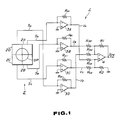
- the focusing error detection circuit operating under the astigmatic system, is arranged as shown in Fig. 13.
- a focusing error detection circuit 1 shown therein, the laser light irradiated on an optical disk, not shown, from an optical pickup, also not shown, is reflected by the disk to form a return beam which then falls on a four-segment photodetector 2 to form a light spot SP.
- light reception outputs S A , S B , S C and S D in the form of light reception currents are outputted from first to fourth photodetector segments 2A, 2B, 2C and 2D of the four-segment photodetector 2.
- the light reception outputs S A , S B , S C and S D are entered into inverting inputs of first to fourth current to voltage converters 3A, 3B, 3C and 3D of the operational amplifier configuration.
- the current to voltage converters 3A to 3D are provided with negative feedback paths including R A1 , R B1 , R C1 and R D1 , respectively, while having their non-inverting inputs grounded.
- First to fourth light reception voltages V A , V B , V C and V D converted from the light reception outputs S A , S B , S C and SD, respectively, are outputted from the output terminals of the converters 3A, 3B, 3C, 3D, respectively.
- the first and the third light reception voltages V A and V C are transmitted via first and third resistors R A2 and R C2 of equal resistance values and summed together before being entered into a non-inverting input of a subtractor 4 of an operational amplifier configuration
- the second and the fourth light reception voltages V B and V D are transmitted via second and fourth resistors R B2 and R D2 of equal resistance values and summed together before being entered into an inverting input of the subtractor 4.
- This subtractor 4 has a negative feedback path including a resistor R1, with its non-inverting input being grounded via resistor R2.
- a differential voltage between the sum voltage of the first and the third light reception voltages V A and V C and the sum voltage of the second and the fourth light reception voltages V B and V D is outputted at an output of the subtractor 4.
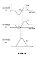
- the focusing error signal S FE is generated so as to have a voltage waveform in the form of a letter S with respect to the distance between the optical disk and the object lens of the optical pickup device.
- the object lens of the optical pickup device is usually controlled by the focusing servo so that the detected focusing error signal S FE will be at a point of intersection P0 between the central portion of the S-shaped voltage waveform and the zero voltage, called a zero-crossing point, such that the laser light of the optical pickup device is irradiated on the optical disk in the just-focusing state, that is in the correctly focused state.
- the above described focusing error detection circuit 1 has a drawback that, should d.c. drift occur due to changes in the operating temperature or the environmental temperature of the operational amplifiers of the substractor 4 and the current to voltage converters 3A to 3D, a d.c. offset proportionate to the d.c. offset is superimposed on the focusing error signal S FE1 itself, as shown at B in Fig.2, to cause fluctuations in the zero-crossing-point P1 and hence in the operating point of the focusing servo.
- the d.c. offset proportionate to the d.c. drift, becomes conspicuous above all in the event of significant changes in temperature, when the volume of the incident light into the four segment photodetector 2 is small or when the broad bandwidth d.c. amplifier circuit configuration operational amplifier is used as the operational amplifier of the subtractor 4, such that the RF signal S RF shown at C in Fig. 2 cannot be reproduced correctly.
- the present invention is directd to a focusing error detection circuit in which the return laser beam which has once been irradiated from the optical pickup on the recording medium and reflected from the recording medium is received by light receiving means, such as a photodetector, to detect the focusing error of the light beam irradiated from the optical pickup device on the recording meduim, wherein, according to the invention, there are provided focusing error computing means for computing focusing errors by arithmetic operation on the basis of a light reception output from said light receiving means to produce a first focusing error signal, sample-and- hold means for sample-holding said first focusing error signal at the timing of periodical trun-off of said laser light to output a sample-held output, and subtraction means for computing the difference between said first focusing error signal and said sample-held signal to produce a second focusing error signal.
- focusing error computing means for computing focusing errors by arithmetic operation on the basis of a light reception output from said light receiving means to produce a first focusing error signal
- the first focusing error signal S FE10 computed by the focusing error computing means 11, is sample-held at the timing of the periodic turning off of the laser light, so that it is only the d.c. drift caused by, for example, the temperture changes of the focusing error computing means, that can be sample-held.
- the sample-held signal is subtracted from the first focusing error signal to produce the second focusing error signal to eliminate the adverse effects of the d.c. drift caused by temperature changes, for example, of the focusing error computing means to enable the focusing error to be detected correctly at all times.
- an error detection circuit 10 includes a four-segment photodetector 22 for detecting the return beam of a laser light irradiated from an optical pickup, not shown, on an optical disk, also not shown, and reflected from the disk.
- the reflected return beam from the disk forms a light spot SP on the four-segment photodetector 22.
- light reception current output signals S A , S B , S C and S D are issued from first, second, third and fourth segment 22A, 22B, 22C and 22D of the four-segment photodetector 22, so as to be entered into a focusing error computing circuit 11.
- This focusing error computing circuit 11 is configured similarly to the focusing error computing circuit of Fig. 1 and adapted to perform an arithmetic operation of the above mentioned formula (1) on the light reception output signals S A to S D from the photodetector 22 to produce a first focusing error signal S FE10 in accordance with the astigmatic system.
- the first focusing error signal S FE10 from the computing circuit 11 is transmitted to a sample-and-hold circuit 12 and a subtractor 13.
- the sample-and-hold circuit 12 operates to sample and hold the first focusing error signal S FE10 , at the timing of a sampling pulse P SH produced by a timing generator 14, and to transmit the thus produced sample-held signal S H to the subtractor 13.
- the subtractor 13 subtracts sample-held signal S M from the first focusing error signal S FE10 and outputs the result as a second focusing error signal S FE11 .
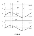
- the timing generator 14 transmits a laser driving signal S LD to a laser driving circuit 15, which laser driving signal is shown at A in Fig. 4 and operates to stop the light emitting operation of the laser driving circuit 15 for a short time during which the focusing servo cannot perform a follow-up movement.
- the timing generator 14 also also transmits sampling pulses P SH , shown at B in Fig. 4, rising at the timing of turning off of the laser, to the sample-and-hold circuit 12.
- the first focusing error signal S FE10 shown at C in Fig. 4 is sampled at the timing of turning off of the laser to sample-and-hold only the DC offset formed by the d.c. drift in the focusing error computing circuit 11 caused by, for example, changes in the temperature.
- the sample-held signal S H formed only by the d.c. offset, as shown at D in Fig. 4, is subtracted from the focusing error signal S FE10 to eliminate the effects by the d.c. drift to enable detection of the focusing error signals S FE10 having perpetually correct waveform as shown at E in Fig. 4.
- the sample-held signal S H is subtracted from the first focusing error signal S FE10 to produce the second focusing error signal S FE11 to eliminate the effects of the d.c. drift caused by, for example, changes in the temperature in the focusing error computing circuit 11 to enable the focusing errors to be detected correctly at all times.
- each operational amplifier of the focusing error computing circuit can be formed by an a.c. amplifier which enables a high-speed arithmetic operation, so that a reliable high-speed focusing servo can be realized.
- the above description has been made of the case of turning off the laser at predetermined constant time periods for a short time during which the focusing servo cannot perform a follow-up movement.
- this is not limiting the present invention.
- the present invention may be so designed that the laser light may be eliminated by the mirror portions of these servo areas.
- the first focusing error output signals from the focusing error computing circuit may be sample-held at the timing of the servo areas before being transmitted to the subtractor.
- the present invention is applied in the above described embodiment to an optical pickup of an optical disk apparatus in which focusing errors are detected by the astigmatic method, it may aslo be applied to other focusing error detecting methods.
- the present invention may also be applied extensively to other optical recording/reproducing apparatus than the optical disk apparatus, such as the magneto-optical disk, optical card or optical tape apparatus.
Abstract
Description
- This invention relates to a focusing error detection circuit which may be employed conveniently with, for example, an optical pickup of an optical disk apparatus.
- In a conventional apparatus for recording and/or reproducing information signals on or from an optical disk, an optical pickup device is employed, in which a light beam from a semiconductor laser collected by an object lens is irradiated on the recording tracks of an optical disk and the reflected return light from the disk is detected to effect readout and/or writing of the information signals.
- Such optical pickup device includes a built-in focusing control unit for controlling an object lens so that the light beam collected by the object lens is irradiated on the recording tracks of the optical lens in the focused state. such focusing control unit performs focusing control by driving a supporting unit, which movably supports the object lens in two directions, that is, along the optical axis of the object lens and along the direction normal to the optical axis and within a horizontal plane, on the basis of the focusing error signals. The supporting unit for supporting the object lens in the two mutually perpendicular directions is shown for example in the US Patent 4473274. The focusing error signals are produced by detecting at a photodetector the state of the reflected return light which is once irradiated on and reflected by the disk surface. For detecting these focusing error signals, there is known a focusing error detection circuit operating in accordance with the astigmatic method such as a disclosed in the US Patent 4023033.
- The focusing error detection circuit, operating under the astigmatic system, is arranged as shown in Fig. 13. Thus, in a focusing
error detection circuit 1, shown therein, the laser light irradiated on an optical disk, not shown, from an optical pickup, also not shown, is reflected by the disk to form a return beam which then falls on a four-segment photodetector 2 to form a light spot SP. - When the return beam falls on the four-segment detector 2 to form the light spot SP, light reception outputs SA, SB, SC and SD in the form of light reception currents are outputted from first to
fourth photodetector segments voltage converters - The current to
voltage converters 3A to 3D are provided with negative feedback paths including RA1, RB1, RC1 and RD1, respectively, while having their non-inverting inputs grounded. First to fourth light reception voltages VA, VB, VC and VD, converted from the light reception outputs SA, SB, SC and SD, respectively, are outputted from the output terminals of theconverters - Of the first to fourth light reception voltage VA to VD, the first and the third light reception voltages VA and VC are transmitted via first and third resistors RA2 and RC2 of equal resistance values and summed together before being entered into a non-inverting input of a subtractor 4 of an operational amplifier configuration, whereas the second and the fourth light reception voltages VB and VD are transmitted via second and fourth resistors RB2 and RD2 of equal resistance values and summed together before being entered into an inverting input of the subtractor 4.
- This subtractor 4 has a negative feedback path including a resistor R₁, with its non-inverting input being grounded via resistor R2. A differential voltage between the sum voltage of the first and the third light reception voltages VA and VC and the sum voltage of the second and the fourth light reception voltages VB and VD is outputted at an output of the subtractor 4. In this manner, with the focusing
error detection circuit 1, the light receiving outputs SA to SD of the four-segment photodetector 2 are computed on the basis of the formula
SFE = (SA+SC) -(SB+SD) (1)
to produce a focusing error signal SFE in accordance with the astigmatic system. - Meanwhile, the focusing error signal SFE is generated so as to have a voltage waveform in the form of a letter S with respect to the distance between the optical disk and the object lens of the optical pickup device.
- Thus the object lens of the optical pickup device is usually controlled by the focusing servo so that the detected focusing error signal SFE will be at a point of intersection P₀ between the central portion of the S-shaped voltage waveform and the zero voltage, called a zero-crossing point, such that the laser light of the optical pickup device is irradiated on the optical disk in the just-focusing state, that is in the correctly focused state.
- The above described focusing
error detection circuit 1 has a drawback that, should d.c. drift occur due to changes in the operating temperature or the environmental temperature of the operational amplifiers of the substractor 4 and the current tovoltage converters 3A to 3D, a d.c. offset proportionate to the d.c. offset is superimposed on the focusing error signal SFE1 itself, as shown at B in Fig.2, to cause fluctuations in the zero-crossing-point P₁ and hence in the operating point of the focusing servo. - The d.c. offset, proportionate to the d.c. drift, becomes conspicuous above all in the event of significant changes in temperature, when the volume of the incident light into the four segment photodetector 2 is small or when the broad bandwidth d.c. amplifier circuit configuration operational amplifier is used as the operational amplifier of the subtractor 4, such that the RF signal SRF shown at C in Fig. 2 cannot be reproduced correctly.
- It is a principal object of the present invention to provide a focusing error detection circuit wherein the adverse effects of d.c. drift caused by temperature changes may be effectively removed to permit the focusing errors to be detected correctly at all times.
- For accomplishing the above object, the present invention is directd to a focusing error detection circuit in which the return laser beam which has once been irradiated from the optical pickup on the recording medium and reflected from the recording medium is received by light receiving means, such as a photodetector, to detect the focusing error of the light beam irradiated from the optical pickup device on the recording meduim, wherein, according to the invention, there are provided focusing error computing means for computing focusing errors by arithmetic operation on the basis of a light reception output from said light receiving means to produce a first focusing error signal, sample-and- hold means for sample-holding said first focusing error signal at the timing of periodical trun-off of said laser light to output a sample-held output, and subtraction means for computing the difference between said first focusing error signal and said sample-held signal to produce a second focusing error signal.
- With the above described focusing error detection circuit, the first focusing error signal SFE10, computed by the focusing error computing means 11, is sample-held at the timing of the periodic turning off of the laser light, so that it is only the d.c. drift caused by, for example, the temperture changes of the focusing error computing means, that can be sample-held. The sample-held signal is subtracted from the first focusing error signal to produce the second focusing error signal to eliminate the adverse effects of the d.c. drift caused by temperature changes, for example, of the focusing error computing means to enable the focusing error to be detected correctly at all times.
- The above and other object and advantages of the present invention will become apparent from the follownig description of the preferred embodiment of the invention which is made in connection with the accompanying drawings.
-
- Fig. 1 is a connection circuit diagram showing a conventional focusing error detection circuit.
- Fig. 2 is a signal waveform diagram for illustrating the operation of the circuit shown in Fig. 1.
- Fig. 3 is a block circuit diagram showing a focusing error detection circuit according to the present invention.
- Fig. 4 is a signal waveform diagram for illustrating the operation of the focusing error detection circuit according to the present invention.
- Referring to Fig. 3, an
error detection circuit 10 according to the present invention includes a four-segment photodetector 22 for detecting the return beam of a laser light irradiated from an optical pickup, not shown, on an optical disk, also not shown, and reflected from the disk. The reflected return beam from the disk forms a light spot SP on the four-segment photodetector 22. - When the return laser light falls on the four-
segment detector 22 to form the light spot SP, light reception current output signals SA, SB, SC and SD are issued from first, second, third andfourth segment segment photodetector 22, so as to be entered into a focusing error computing circuit 11. - This focusing error computing circuit 11 is configured similarly to the focusing error computing circuit of Fig. 1 and adapted to perform an arithmetic operation of the above mentioned formula (1) on the light reception output signals SA to SD from the
photodetector 22 to produce a first focusing error signal SFE10 in accordance with the astigmatic system. - With the
present detection circuit 10, the first focusing error signal SFE10 from the computing circuit 11 is transmitted to a sample-and-hold circuit 12 and asubtractor 13. - The sample-and-
hold circuit 12 operates to sample and hold the first focusing error signal SFE10, at the timing of a sampling pulse PSH produced by atiming generator 14, and to transmit the thus produced sample-held signal SH to thesubtractor 13. - The
subtractor 13 subtracts sample-held signal SM from the first focusing error signal SFE10 and outputs the result as a second focusing error signal SFE11. - At predetermined constant time intervals, the
timing generator 14 transmits a laser driving signal SLD to alaser driving circuit 15, which laser driving signal is shown at A in Fig. 4 and operates to stop the light emitting operation of thelaser driving circuit 15 for a short time during which the focusing servo cannot perform a follow-up movement. Thetiming generator 14 also also transmits sampling pulses PSH, shown at B in Fig. 4, rising at the timing of turning off of the laser, to the sample-and-hold circuit 12. - Thus, with the present embodiment, the first focusing error signal SFE10 shown at C in Fig. 4 is sampled at the timing of turning off of the laser to sample-and-hold only the DC offset formed by the d.c. drift in the focusing error computing circuit 11 caused by, for example, changes in the temperature. The sample-held signal SH, formed only by the d.c. offset, as shown at D in Fig. 4, is subtracted from the focusing error signal SFE10 to eliminate the effects by the d.c. drift to enable detection of the focusing error signals SFE10 having perpetually correct waveform as shown at E in Fig. 4.
- With the above described focusing error detection circuit, according to the present invention, the sample-held signal SH is subtracted from the first focusing error signal SFE10 to produce the second focusing error signal SFE11 to eliminate the effects of the d.c. drift caused by, for example, changes in the temperature in the focusing error computing circuit 11 to enable the focusing errors to be detected correctly at all times.
- Also, with the above construction, the d.c. components can be reproduced even when the focusing error computing circuit is the a.c. coupled circuit. Therefore, with the focusing error detection circuit according to the present invention, each operational amplifier of the focusing error computing circuit can be formed by an a.c. amplifier which enables a high-speed arithmetic operation, so that a reliable high-speed focusing servo can be realized.
- The above description has been made of the case of turning off the laser at predetermined constant time periods for a short time during which the focusing servo cannot perform a follow-up movement. However, this is not limiting the present invention. For example, when the recording tracks on the optical disk are formed in accordance with a so-called sample format system in which servo areas are provided at intervals of a predetermined period, the present invention may be so designed that the laser light may be eliminated by the mirror portions of these servo areas.
- In this case, since the focusing servo operation itself is performed in the servo areas, the first focusing error output signals from the focusing error computing circuit may be sample-held at the timing of the servo areas before being transmitted to the subtractor.
- When video signals, for example, are recorded on the optical disk, the effects similar to those achieved in the above embodiment may be achieved by turning off the laser light at each vertical blanking period.
- Although the present invention is applied in the above described embodiment to an optical pickup of an optical disk apparatus in which focusing errors are detected by the astigmatic method, it may aslo be applied to other focusing error detecting methods. The present invention may also be applied extensively to other optical recording/reproducing apparatus than the optical disk apparatus, such as the magneto-optical disk, optical card or optical tape apparatus.
Claims (6)
focusing error computing means (11) for processing focusing errors by arithmetic operation on the basis of an output from said tight receiving means to produce a first focusing error signal (SFE10),
sample-and-hold means (12) for sample-holding said first focusing error signal at the timing of periodical turn-off of said laser light to output a sample-held output (SH), and
second focusing error computing means (13) for computing the difference between said first focusing error signal and said sample-held signal to produce a second focusing error signal (SFE11).
Applications Claiming Priority (2)
| Application Number | Priority Date | Filing Date | Title |
|---|---|---|---|
| JP63315673A JP2701392B2 (en) | 1988-12-14 | 1988-12-14 | Focus error detection circuit |
| JP315673/88 | 1988-12-14 |
Publications (3)
| Publication Number | Publication Date |
|---|---|
| EP0373607A2 true EP0373607A2 (en) | 1990-06-20 |
| EP0373607A3 EP0373607A3 (en) | 1991-08-07 |
| EP0373607B1 EP0373607B1 (en) | 1994-04-13 |
Family
ID=18068195
Family Applications (1)
| Application Number | Title | Priority Date | Filing Date |
|---|---|---|---|
| EP89122962A Expired - Lifetime EP0373607B1 (en) | 1988-12-14 | 1989-12-12 | Focusing error detection circuit |
Country Status (5)
| Country | Link |
|---|---|
| US (1) | US4992652A (en) |
| EP (1) | EP0373607B1 (en) |
| JP (1) | JP2701392B2 (en) |
| KR (1) | KR0175292B1 (en) |
| DE (1) | DE68914615T2 (en) |
Cited By (2)
| Publication number | Priority date | Publication date | Assignee | Title |
|---|---|---|---|---|
| EP0536558A1 (en) * | 1991-10-09 | 1993-04-14 | Nippon Conlux Co., Ltd. | Apparatus for optically recording and reproducing information |
| EP1675109A3 (en) * | 2004-12-27 | 2006-12-06 | Kabushiki Kaisha Toshiba | Optical disc recording/reproducing apparatus |
Families Citing this family (5)
| Publication number | Priority date | Publication date | Assignee | Title |
|---|---|---|---|---|
| JP2613118B2 (en) * | 1990-04-10 | 1997-05-21 | 富士写真フイルム株式会社 | Confocal scanning microscope |
| JP2716569B2 (en) * | 1990-04-25 | 1998-02-18 | パイオニア株式会社 | Optical information reader |
| US6252835B1 (en) | 1996-09-19 | 2001-06-26 | L G Electronics Inc | Apparatus for automatically adjusting focus offset and method thereof in a disc player |
| KR100447663B1 (en) * | 1996-09-19 | 2004-11-08 | 엘지전자 주식회사 | Device for automatically controlling a cdp focus offset and a method therefor, particularly enabling a reliable automatic control for abnormal conditions such as scars and dust of a disk |
| WO2006021931A1 (en) * | 2004-08-27 | 2006-03-02 | Koninklijke Philips Electronics N.V. | System for scribing a visible label |
Citations (3)
| Publication number | Priority date | Publication date | Assignee | Title |
|---|---|---|---|---|
| US4023033A (en) * | 1974-01-15 | 1977-05-10 | Thomson-Brandt | Optical focussing device |
| JPS60119642A (en) * | 1983-11-30 | 1985-06-27 | Ricoh Co Ltd | Optical information recording and reproducing device |
| DE3723923A1 (en) * | 1987-05-09 | 1988-11-24 | Thomson Brandt Gmbh | Device for the reproduction of data |
Family Cites Families (7)
| Publication number | Priority date | Publication date | Assignee | Title |
|---|---|---|---|---|
| JPS5877036A (en) * | 1981-10-30 | 1983-05-10 | Olympus Optical Co Ltd | Detecting method of tracking error |
| JPS58121139A (en) * | 1982-01-11 | 1983-07-19 | Olympus Optical Co Ltd | Automatic focus controller |
| JPS58199307A (en) * | 1982-05-18 | 1983-11-19 | Olympus Optical Co Ltd | Focusing detecting device |
| JPS58208944A (en) * | 1982-05-31 | 1983-12-05 | Sony Corp | Generating device of optical head control signal |
| JPS6070924U (en) * | 1983-10-19 | 1985-05-20 | パイオニア株式会社 | Focus error detection device |
| JPS60185230A (en) * | 1984-03-02 | 1985-09-20 | Pioneer Electronic Corp | Focal error detector |
| DE3678311D1 (en) * | 1985-02-15 | 1991-05-02 | Hitachi Ltd | OPTICAL DISK DEVICE. |
-
1988
- 1988-12-14 JP JP63315673A patent/JP2701392B2/en not_active Expired - Fee Related
-
1989
- 1989-12-05 US US07/446,444 patent/US4992652A/en not_active Expired - Lifetime
- 1989-12-11 KR KR1019890018273A patent/KR0175292B1/en not_active IP Right Cessation
- 1989-12-12 DE DE68914615T patent/DE68914615T2/en not_active Expired - Fee Related
- 1989-12-12 EP EP89122962A patent/EP0373607B1/en not_active Expired - Lifetime
Patent Citations (3)
| Publication number | Priority date | Publication date | Assignee | Title |
|---|---|---|---|---|
| US4023033A (en) * | 1974-01-15 | 1977-05-10 | Thomson-Brandt | Optical focussing device |
| JPS60119642A (en) * | 1983-11-30 | 1985-06-27 | Ricoh Co Ltd | Optical information recording and reproducing device |
| DE3723923A1 (en) * | 1987-05-09 | 1988-11-24 | Thomson Brandt Gmbh | Device for the reproduction of data |
Non-Patent Citations (2)
| Title |
|---|
| IBM TECHNICAL DISCLOSURE BULLETIN vol. 30, no. 2, July 1987, New York, USA "FINE FOCUSING ONTO AN OPTICAL DISK" * |
| PATENT ABSTRACTS OF JAPAN vol. 9, no. 276 (P-402)(1999) 02 November 1985, & JP-A-60 119642 (RICOH K K) 27 June 1985, * |
Cited By (3)
| Publication number | Priority date | Publication date | Assignee | Title |
|---|---|---|---|---|
| EP0536558A1 (en) * | 1991-10-09 | 1993-04-14 | Nippon Conlux Co., Ltd. | Apparatus for optically recording and reproducing information |
| EP1675109A3 (en) * | 2004-12-27 | 2006-12-06 | Kabushiki Kaisha Toshiba | Optical disc recording/reproducing apparatus |
| KR100783452B1 (en) | 2004-12-27 | 2007-12-07 | 가부시끼가이샤 도시바 | Optical disc recording/reproducing apparatus |
Also Published As
| Publication number | Publication date |
|---|---|
| EP0373607B1 (en) | 1994-04-13 |
| US4992652A (en) | 1991-02-12 |
| DE68914615D1 (en) | 1994-05-19 |
| EP0373607A3 (en) | 1991-08-07 |
| JPH02161623A (en) | 1990-06-21 |
| JP2701392B2 (en) | 1998-01-21 |
| DE68914615T2 (en) | 1994-10-06 |
| KR900010691A (en) | 1990-07-09 |
| KR0175292B1 (en) | 1999-04-15 |
Similar Documents
| Publication | Publication Date | Title |
|---|---|---|
| EP0102607B1 (en) | Disc playback apparatus | |
| US4616354A (en) | Tracking control arrangements for use in optical disc players | |
| KR19980033329A (en) | Track detection circuit of optical disc reproducing apparatus | |
| EP0087973B1 (en) | Tracking servo system for optical-disc information reproducing apparatus | |
| EP0512616B1 (en) | Optical scanning device | |
| EP0813191A2 (en) | Circuit for generating a track traverse detecting signal in an information recording and reproducing apparatus for an optical information recording medium | |
| EP0373607B1 (en) | Focusing error detection circuit | |
| EP0497548B1 (en) | Apparatus for detecting position of light spot | |
| ATE157796T1 (en) | OPTICAL SCANNING DEVICE | |
| US4426690A (en) | Optical reproducing device having focus servo system | |
| US4603410A (en) | Error signal generating device for use in an apparatus for optically reading information with a resistance network connected to photo detector elements | |
| US4794244A (en) | Method and apparatus for detecting focussing position deviation of read/write apparatus in an optical recording medium | |
| KR100244772B1 (en) | Tracking servo of digital video disc rewrite system | |
| JPS63164026A (en) | Information processor | |
| JP2925807B2 (en) | Track crossing detection signal forming circuit for optical information recording medium | |
| KR870000598B1 (en) | Tracking error signal producing apparatus | |
| KR0165597B1 (en) | Disk tilt detection device of optic disk reproducing system | |
| JP2692060B2 (en) | Recording and playback device | |
| KR950000127B1 (en) | Track jump/seek control device & method of position error rivision | |
| JPS6132228A (en) | Detection system for tracking error signal | |
| JPH0376031A (en) | Track polarity detector | |
| JPH0227735B2 (en) | ||
| JPS61940A (en) | Method of tracking of optical disk reproducing device | |
| JPS58185044A (en) | Disk reproducer | |
| JPH0714181A (en) | Optical disk device |
Legal Events
| Date | Code | Title | Description |
|---|---|---|---|
| PUAI | Public reference made under article 153(3) epc to a published international application that has entered the european phase |
Free format text: ORIGINAL CODE: 0009012 |
|
| AK | Designated contracting states |
Kind code of ref document: A2 Designated state(s): DE FR GB NL |
|
| PUAL | Search report despatched |
Free format text: ORIGINAL CODE: 0009013 |
|
| AK | Designated contracting states |
Kind code of ref document: A3 Designated state(s): DE FR GB NL |
|
| 17P | Request for examination filed |
Effective date: 19920108 |
|
| 17Q | First examination report despatched |
Effective date: 19930629 |
|
| GRAA | (expected) grant |
Free format text: ORIGINAL CODE: 0009210 |
|
| AK | Designated contracting states |
Kind code of ref document: B1 Designated state(s): DE FR GB NL |
|
| REF | Corresponds to: |
Ref document number: 68914615 Country of ref document: DE Date of ref document: 19940519 |
|
| ET | Fr: translation filed | ||
| PLBE | No opposition filed within time limit |
Free format text: ORIGINAL CODE: 0009261 |
|
| STAA | Information on the status of an ep patent application or granted ep patent |
Free format text: STATUS: NO OPPOSITION FILED WITHIN TIME LIMIT |
|
| 26N | No opposition filed | ||
| PGFP | Annual fee paid to national office [announced via postgrant information from national office to epo] |
Ref country code: GB Payment date: 20011212 Year of fee payment: 13 Ref country code: FR Payment date: 20011212 Year of fee payment: 13 |
|
| PGFP | Annual fee paid to national office [announced via postgrant information from national office to epo] |
Ref country code: NL Payment date: 20011228 Year of fee payment: 13 |
|
| REG | Reference to a national code |
Ref country code: GB Ref legal event code: IF02 |
|
| PGFP | Annual fee paid to national office [announced via postgrant information from national office to epo] |
Ref country code: DE Payment date: 20020109 Year of fee payment: 13 |
|
| PG25 | Lapsed in a contracting state [announced via postgrant information from national office to epo] |
Ref country code: GB Free format text: LAPSE BECAUSE OF NON-PAYMENT OF DUE FEES Effective date: 20021212 |
|
| PG25 | Lapsed in a contracting state [announced via postgrant information from national office to epo] |
Ref country code: NL Free format text: LAPSE BECAUSE OF NON-PAYMENT OF DUE FEES Effective date: 20030701 Ref country code: DE Free format text: LAPSE BECAUSE OF NON-PAYMENT OF DUE FEES Effective date: 20030701 |
|
| GBPC | Gb: european patent ceased through non-payment of renewal fee | ||
| NLV4 | Nl: lapsed or anulled due to non-payment of the annual fee |
Effective date: 20030701 |
|
| PG25 | Lapsed in a contracting state [announced via postgrant information from national office to epo] |
Ref country code: FR Free format text: LAPSE BECAUSE OF NON-PAYMENT OF DUE FEES Effective date: 20030901 |
|
| REG | Reference to a national code |
Ref country code: FR Ref legal event code: ST |