EP0368417B1 - Anordnung mit einer verbesserten Gleichstrompegelauswertungsvorrichtung - Google Patents
Anordnung mit einer verbesserten Gleichstrompegelauswertungsvorrichtung Download PDFInfo
- Publication number
- EP0368417B1 EP0368417B1 EP89202825A EP89202825A EP0368417B1 EP 0368417 B1 EP0368417 B1 EP 0368417B1 EP 89202825 A EP89202825 A EP 89202825A EP 89202825 A EP89202825 A EP 89202825A EP 0368417 B1 EP0368417 B1 EP 0368417B1
- Authority
- EP
- European Patent Office
- Prior art keywords
- signal
- circuit
- received
- value
- correction signal
- Prior art date
- Legal status (The legal status is an assumption and is not a legal conclusion. Google has not performed a legal analysis and makes no representation as to the accuracy of the status listed.)
- Expired - Lifetime
Links
Images
Classifications
-
- H—ELECTRICITY
- H04—ELECTRIC COMMUNICATION TECHNIQUE
- H04N—PICTORIAL COMMUNICATION, e.g. TELEVISION
- H04N7/00—Television systems
- H04N7/08—Systems for the simultaneous or sequential transmission of more than one television signal, e.g. additional information signals, the signals occupying wholly or partially the same frequency band, e.g. by time division
- H04N7/083—Systems for the simultaneous or sequential transmission of more than one television signal, e.g. additional information signals, the signals occupying wholly or partially the same frequency band, e.g. by time division with signal insertion during the vertical and the horizontal blanking interval, e.g. MAC data signals
-
- H—ELECTRICITY
- H04—ELECTRIC COMMUNICATION TECHNIQUE
- H04N—PICTORIAL COMMUNICATION, e.g. TELEVISION
- H04N9/00—Details of colour television systems
- H04N9/64—Circuits for processing colour signals
Definitions
- the present invention relates to an apparatus intended to receive a signal conveying analog luminance and chrominance information associated with periods of coded digital signal, provided with a device for restoring the DC component and a decoder circuit for decoding the signal. digital received.
- a signal is in particular a MAC type signal, which comprises analog luminance and chrominance information and digital information coded in packets as well as analog voltage reference steps of medium gray level.
- Such a device is for example a television equipped for the reception of a signal in D2-MAC / packet, or else a "satellite tuner" or even any device provided with a body performing a signal processing in a system of transmission.
- a television set is provided with means for restoring the continuous component, in different successive and mutually exclusive stages, first from the peak levels measured over the entire signal, then from the peak levels measured only over the part of the signal that is digital, and finally from the reference voltage stages of the signal.
- the so-called “continuous” component which also includes a low frequency component, is affected by the disturbances inherent in any transmission system, whether or not they are correlated with the television signal.
- These disturbances constitute a parasitic signal comprising two components, the low frequency noise in front of the line frequency (low frequency break, energy dispersion, 50 Hz residue, etc.), and the noise of modulation whose spectral power distribution depends on the type of transmission.
- the device for restoring the DC component comprises a coding member carrying out from the decoded digital signal a coding identical to that used for the creation of the received signal, a circuit for estimating the DC component calculating said estimate at starting from the differences between the received coded signal and the coded signal reconstructed by the above coding member, this estimation constituting a DC component correction signal, and a subtractor circuit for subtracting from the received signal said correction signal, over the entire duration d 'a line.
- the device advantageously comprises downstream of the DC component estimation circuit a filter using the correction signals from several line scanning periods at the same time to refine the correction signal, before its subtraction from the signal received in the subtractor circuit.
- this filter being of the finite impulse response type, for example an averager, and a delay circuit of the received signal placed downstream of the subtractor circuit, to compensate for the delay due to the filter.
- the invention is therefore based on the principle of extracting additional information on the low frequency component of the signal by efficiently exploiting the digital period, and on the other hand integrating this information over several lines using a filter. suitable preserving the low frequency component.
- the apparatus is also advantageously provided, at the input of the decoder, with a subtraction circuit in which the correction signal is subtracted from the received signal. This has the effect of increasing the reliability of the decoding.
- Another important characteristic of the invention is based on the remark that the presence of the coding member allows an estimation of the reliability of the received signal.
- the device is therefore advantageously provided with a validation circuit which, from the measurement of the difference between the received signal and the reconstructed signal, controls the taking into account of the correction signal.
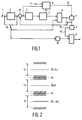
- FIG. 1 is a block diagram of the preferred embodiment of a device for restoring the DC component in an apparatus according to the invention.
- FIG. 2 illustrates the levels which are taken into account for decision and recoding in the case of a duobinary type signal, and of a threshold decoder.
- an amplified signal for example of the D2-MAC-Packet type, which first presents a period of digital data coded in duobinary whose duration is 10 "s, then a reference level of the average gray level which lasts only 0.75 ”s, followed by an analog signal period representing the chrominance information and an analog signal period representing the luminance information which terminates the line.
- the amplified signal available at 1 is brought first of all to a conventional DC voltage alignment device 2 based on the line bearings.
- the device then includes a decoder for digital data 3, then a coding member 4 for this data of the type used to create the received signal.
- the digital data decoder 3 can conventionally take the form of a low-pass filter with a cutoff frequency of 5 MHz followed by a threshold decoder or possibly a Viterbi decoder.
- An associated circuit 5 makes it possible to measure the validity of the reconstructed digital signal based on the signal present at the input of the decoder 3.
- the reconstructed coded digital signal is compared in the estimation circuit 6 with the available signal, the latter being taken either at the input 1 or at the output of the conventional DC voltage alignment system 2, this choice being symbolized in the figure by an inverter 18 which is not required to exist physically, a final choice of connection being able to be done by construction. From this comparison, the estimation circuit 6 forms a correction signal.
- the estimation circuit 6 is a circuit which subtracts the received signal and the reconstructed signal from each other.
- the estimation circuit 6 is followed by a filtering circuit 7.
- circuit 7 has information extracted from the duobinary burst and supplied by circuit 6, which allows, when validated, to reconstruct the low frequency component.
- This circuit 7, which takes, in a preferred embodiment, the form of a simple averager, provides a value-result per line.
- the correction signal is subtracted from the signal received at the input of the decoder 3, in a subtraction circuit 19. Depending on the position of the inverter 15, the signal thus subtracted is either the signal available at the output of the estimation circuit 6, or that available at the output of the filtering circuit 7.
- the inverter 15 may not exist in the case where a final connection is chosen during construction.
- the value-result from the filtering circuit 7 is then processed by a circuit 8 in order to refine its value by weighting it by those obtained for the preceding lines.
- This circuit which is a filter can either be of the recursive type and deliver information synchronous with the current line, or deliver information delayed by the duration of an integer number of lines.
- the correction signal is subtracted by the subtractor circuit 9, over the entire duration of a line, from the available signal, either at input 1, or possibly at output from the conventional DC voltage alignment system. 2, this signal possibly being delayed (depending on the delay of the line filter) in a circuit 10 in order to ensure the synchronization of the two signals.
- FIG. 2 in which the references 14 indicate decision thresholds and the references 13 indicate three ranges of the same width, said width defining a reliability threshold, illustrates the reconstruction of the duobinary train in the case where the element 3 is a decoder with threshold.
- This reconstruction is summarized by the following logical operations: if
- the control circuit 5 provides an estimate of the reliability of the reconstruction of the duobinary signal in the form of a validation signal 12 intended for the filtering module 7. It does this in the following manner: the reconstructed signal is compared to the duobinary signal present at the input of the decoder, and a voltage applied at 11 defines a reliability threshold which represents the maximum authorized difference between the two signals beyond which the reconstructed sample will no longer be taken into account in the calculation of the component low frequency. For example in the case of a decoding / recoding in D2-MAC-packet, which relates to one hundred and five bits per line, the decision of taking into account or not is taken for each of these one hundred and five bits.
- the device is provided with a validation circuit which, from the measurement of the difference between the received signal and the reconstructed signal, controls the taking into account of the correction signal.
- the circuit 8 making it possible to weight the information coming from the filter 7 by the values obtained on the preceding lines takes the form of a non-recursive filter called "Finite Impulse Response".
- the advantage of this filter is to have a response whose delay with respect to the input data is fixed for a given filter length and can thus be compensated to ensure perfect synchronization.
- a simple and advantageous embodiment is constituted by an averager which preferably acts on an odd number of data.
- the delay generated by the averager is equal to its half-length, and is therefore equal to (N-1) / 2 line periods if the filter acts on N data.
- the circuit 10 delays by this value the signal available at the input 1 or possibly at the output of the conventional DC voltage alignment system 2.
Claims (9)
- Vorrichtung zum Empfangen eines Signals, mit dem einzelnen numerischen kodierten Signalperioden zugeordnete analoge Helligkeits- und Chrominanzinformationen übertragen werden, mit einer Vorrichtung zur Auswertung der Gleichstromkomponente und einer Dekodierschaltung (3) zum Dekodieren des empfangenen numerischen Signals, dadurch gekennzeichnet, daß die Vorrichtung zur Wiederherstellung der Gleichstromkomponente ein Kodierelement (4) umfaßt, das ausgehend von dem dekodierten numerischen Signal eine Kodierung gleich der vornimmt, wie sie für die Erzeugung des empfangenen Signals verwendet wird, ferner eine Auswerteschaltung (6) für die Gleichstromkomponente, die deren Wert aus Differenzen zwischen dem empfangenen kodierten Signal (1) und dem durch das vorgenannte Kodierelement (4) wiederhergestellten kodierten Signal berechnet, wobei der so errechnete Wert ein Gleichstromkomponenten-Korrektursignal darstellt, und eine Subtraktionsschaltung (9), mittels derer das Korrektursignal über die gesamte Dauer einer Zeile hinweg vom empfangenen Signal abgezogen wird.
- Vorrichtung nach Anspruch 1, dadurch gekennzeichnet, daß sie mit einer der Auswerteschaltung (6) nachgeschalteten Filterschaltung (7) ausgestattet ist.
- Vorrichtung nach Anspruch 2, dadurch gekennzeichnet, daß die Filterschaltung (7) aus einer einfachen Mittelungsschaltung besteht.
- Vorrichtung nach Anspruch 1, dadurch gekennzeichnet, daß die Vorrichtung ein der Auswerteschaltung (6) für die Gleichstromkomponente nachgeschaltetes Filter (8) umfaßt, das gleichzeitig die Korrektursignale mehrerer Zeilenabtastperioden zum Abgleich des Korrektursignals verwendet, bevor dieses in der Subtraktionsschaltung (9) vom empfangenen Signal abgezogen wird, wobei dieses Filter als Filter mit endlicher Impulscharakteristik, zum Beispiel als Mittelungsschaltung, ausgebildet ist, und der Subtraktionsschaltung (9) eine Verzögerungsschaltung (10) für das empfangene Signal zum Ausgleich der durch das Filter (8) bedingten Verzögerung vorgeschaltet ist.
- Vorrichtung nach einem der vorhergehenden Ansprüche, dadurch gekennzeichnet, daß die Vorrichtung ferner am Eingang des Dekodierers (3) mit einer Subtraktionsschaltung (19) ausgestattet ist, in der das Korrektursignal vom empfangenen Signal abgezogen wird.
- Vorrichtung nach einem der vorhergehenden Ansprüche mit einem Schwellwertdekoder als Dekoder (3), dadurch gekennzeichnet, daß das Kodierelement (4) eine logische Schaltung ist, die die folgenden logischen Operationen ausführt:
Wenn |ck-Cc| < Entscheidungsschwelle, dann ĉk = 0,
wenn ck-Cc < negative Entscheidungsschwelle, dann nimmt ĉk einen negativen Standardwert an,
wenn ck-Cc > positive Entscheidungsschwelle, dann nimmt ĉk einen positiven Standardwert an,
wobei ck der Wert der empfangenen doppelt-binären Probe,
ĉk der Wert der wiederhergestellten doppelt-binären Probe und Cc der Wert des Korrektursignals ist. - Vorrichtung nach einem der Ansprüche 1 bis 6, dadurch gekennzeichnet, daß sie mit einer Validierungsschaltung (5) ausgestattet ist, die ausgehend von der Messung des Abstandes zwischen dem empfangenen Signal und dem wiederhergestellten Signal die Berücksichtigung des Korrektursignals steuert.
- Vorrichtung nach Anspruch 7, dadurch gekennzeichnet, daß die Validierungsschaltung (5) die Berücksichtigung des Kurrektursignals steuert, wenn |ck-Cc-ĉk| kleiner ist als ein vorbestimmter Zuverlässigkeits-Schwellwert, wobei ck der Wert der empfangenen doppelt-binären Probe, ĉk der Wert der wiederhergestellten doppelt-binären Probe und Cc der Wert des Korrektursignals ist.
- Vorrichtung nach einem der vorhergehenden Ansprüche, dadurch gekennzeichnet, daß sie im übrigen mit einer dem Dekoder vorgeschalteten Vorrichtung (2) zum Gleichspannungsabgleich auf der Grundlage der im empfangenen Signal enthaltenen analogen Gleichspannungsstufen ausgestattet ist.
Applications Claiming Priority (4)
| Application Number | Priority Date | Filing Date | Title |
|---|---|---|---|
| FR8814685A FR2638925B1 (fr) | 1988-11-10 | 1988-11-10 | Appareil muni d'un dispositif de restitution de la composante continue ameliore |
| FR8814685 | 1988-11-10 | ||
| FR8907097A FR2647996B3 (fr) | 1989-05-30 | 1989-05-30 | Appareil muni d'un dispositif de restitution de la composante continue ameliore |
| FR8907097 | 1989-05-30 |
Publications (2)
| Publication Number | Publication Date |
|---|---|
| EP0368417A1 EP0368417A1 (de) | 1990-05-16 |
| EP0368417B1 true EP0368417B1 (de) | 1995-02-01 |
Family
ID=26226981
Family Applications (1)
| Application Number | Title | Priority Date | Filing Date |
|---|---|---|---|
| EP89202825A Expired - Lifetime EP0368417B1 (de) | 1988-11-10 | 1989-11-08 | Anordnung mit einer verbesserten Gleichstrompegelauswertungsvorrichtung |
Country Status (7)
| Country | Link |
|---|---|
| US (1) | US5036388A (de) |
| EP (1) | EP0368417B1 (de) |
| JP (1) | JPH02214269A (de) |
| KR (1) | KR900008880A (de) |
| DE (1) | DE68920953T2 (de) |
| ES (1) | ES2070171T3 (de) |
| HK (1) | HK66896A (de) |
Families Citing this family (3)
| Publication number | Priority date | Publication date | Assignee | Title |
|---|---|---|---|---|
| FR2675331A1 (fr) * | 1991-04-12 | 1992-10-16 | Philips Electro Grand Public | Appareil muni d'un dispositif ameliore de restitution de la composante continue. |
| WO1999014866A2 (en) * | 1997-09-12 | 1999-03-25 | Koninklijke Philips Electronics N.V. | Transmission system with improved reconstruction of missing parts |
| US20030219085A1 (en) * | 2001-12-18 | 2003-11-27 | Endres Thomas J. | Self-initializing decision feedback equalizer with automatic gain control |
Family Cites Families (4)
| Publication number | Priority date | Publication date | Assignee | Title |
|---|---|---|---|---|
| JPS57208770A (en) * | 1981-06-19 | 1982-12-21 | Hitachi Ltd | Dc level automatic compensating circuit for analog signal repetitively including reference level signal |
| FR2565448B1 (fr) * | 1984-06-04 | 1986-10-10 | France Etat | Procede et dispositif d'extraction de synchronisation pour systeme de diffusion a multiplexage temporel de signaux numeriques et analogiques |
| US4713694A (en) * | 1985-09-09 | 1987-12-15 | Hughes Aircraft Company | Noninvasive DC restoration to upgrade AC coupled systems |
| FR2610773B1 (fr) * | 1987-02-06 | 1989-05-26 | Radiotechnique Ind & Comm | Systeme de synchronisation sur un signal semi-numerique |
-
1989
- 1989-11-03 US US07/431,499 patent/US5036388A/en not_active Expired - Fee Related
- 1989-11-08 EP EP89202825A patent/EP0368417B1/de not_active Expired - Lifetime
- 1989-11-08 DE DE68920953T patent/DE68920953T2/de not_active Expired - Fee Related
- 1989-11-08 JP JP1288936A patent/JPH02214269A/ja active Pending
- 1989-11-08 ES ES89202825T patent/ES2070171T3/es not_active Expired - Lifetime
- 1989-11-10 KR KR1019890016253A patent/KR900008880A/ko not_active Application Discontinuation
-
1996
- 1996-04-18 HK HK66896A patent/HK66896A/xx not_active IP Right Cessation
Also Published As
| Publication number | Publication date |
|---|---|
| ES2070171T3 (es) | 1995-06-01 |
| US5036388A (en) | 1991-07-30 |
| DE68920953T2 (de) | 1995-08-31 |
| DE68920953D1 (de) | 1995-03-16 |
| KR900008880A (ko) | 1990-06-04 |
| JPH02214269A (ja) | 1990-08-27 |
| HK66896A (en) | 1996-04-26 |
| EP0368417A1 (de) | 1990-05-16 |
Similar Documents
| Publication | Publication Date | Title |
|---|---|---|
| EP0246701B1 (de) | DPCM-Kodierer und zugehöriger Dekodierer | |
| EP0022723A1 (de) | Verfahren und Vorrichtung zur Rückgewinnung digitaler Daten bei Anwesenheit von Rauschen und Verzerrungen | |
| FR2596221A1 (fr) | Systeme de filtre median adaptif | |
| EP0421897B1 (de) | Vorrichtung zum Extrahieren von digitalen Daten aus einem Video-Signal | |
| EP0159924A1 (de) | Digitaler "DIDON"-Demodulator | |
| EP0418952A1 (de) | Vorrichtung zum Codieren von zweidimensionalen Informationen und entsprechende Decodiervorrichtung | |
| EP0337565B1 (de) | Einrichtung zur Kodierung von Signalen, die eine Folge von Bildern darstellen und Übertragungssystem von Fernsehbildern mit hoher Auflösung mit einer solchen Einrichtung | |
| EP0869476B1 (de) | Vorrichtung zur Erzeugung von Hintergrundrauschen | |
| EP0368417B1 (de) | Anordnung mit einer verbesserten Gleichstrompegelauswertungsvorrichtung | |
| EP0078195B1 (de) | Verfahren und System zur differentiellen Kodierung und Dekodierung von Daten mit Begrenzung der Fortpflanzung von Übertragungsfehlern | |
| FR2647996A3 (fr) | Appareil muni d'un dispositif de restitution de la composante continue ameliore | |
| EP0030194B1 (de) | Prediktorstufe für ein System zur Kompression des Datenflusses | |
| EP0063990A1 (de) | Verfahren zur Bildübertragung mit beschränktem Datafluss; Übertragungssystem zur Durchführung dieses Verfahrens | |
| FR2638925A1 (fr) | Appareil muni d'un dispositif de restitution de la composante continue ameliore | |
| EP0348322B1 (de) | Verfahren zur Auswertung des Gleichstrompegels eines Signals nach der DMAC-Paket-Norm, entsprechende Vorrichtung und Benutzung | |
| EP0528738B1 (de) | Verfahren und Schaltung zur Koeffizientenanpassung im Entzerrer eines Modems | |
| EP0511698A1 (de) | Halbrekursiver adaptiver Entzerrer | |
| EP0905946B1 (de) | Reglung der Abtastung von Biphasensignalen | |
| FR2690032A1 (fr) | Procédé d'alignement en télévision et dispositif pour sa mise en Óoeuvre. | |
| EP0283077A1 (de) | Einrichtung zur Dekodierung duobinärer kodierter Signale | |
| EP0160595B1 (de) | Schaltungsanordnung zum Kodieren und Dekodieren eines Videosignals, kodiert durch Verschiebung des Bildsignals hinsichtlich des Synchronisiersignals | |
| FR2675331A1 (fr) | Appareil muni d'un dispositif ameliore de restitution de la composante continue. | |
| FR2595896A1 (fr) | Dispositif de decodage numerique de signaux de television a moyens adaptatifs de separation de la luminance et de la chrominance | |
| CA2019774C (fr) | Dispositif de detection dans un signal binaire d'une signalisation formee nominalement d'une serie continue d'elements binaires de meme valeur | |
| EP0295974B1 (de) | Verfahren und Gerät zum Dekodieren von duobinären Signalen, übertragen mittels Salven |
Legal Events
| Date | Code | Title | Description |
|---|---|---|---|
| PUAI | Public reference made under article 153(3) epc to a published international application that has entered the european phase |
Free format text: ORIGINAL CODE: 0009012 |
|
| AK | Designated contracting states |
Kind code of ref document: A1 Designated state(s): DE ES FR GB IT |
|
| 17P | Request for examination filed |
Effective date: 19901114 |
|
| 17Q | First examination report despatched |
Effective date: 19930625 |
|
| GRAA | (expected) grant |
Free format text: ORIGINAL CODE: 0009210 |
|
| AK | Designated contracting states |
Kind code of ref document: B1 Designated state(s): DE ES FR GB IT |
|
| REF | Corresponds to: |
Ref document number: 68920953 Country of ref document: DE Date of ref document: 19950316 |
|
| ITF | It: translation for a ep patent filed |
Owner name: ING. C. GREGORJ S.P.A. |
|
| GBT | Gb: translation of ep patent filed (gb section 77(6)(a)/1977) |
Effective date: 19950420 |
|
| REG | Reference to a national code |
Ref country code: ES Ref legal event code: FG2A Ref document number: 2070171 Country of ref document: ES Kind code of ref document: T3 |
|
| PLBE | No opposition filed within time limit |
Free format text: ORIGINAL CODE: 0009261 |
|
| STAA | Information on the status of an ep patent application or granted ep patent |
Free format text: STATUS: NO OPPOSITION FILED WITHIN TIME LIMIT |
|
| 26N | No opposition filed | ||
| REG | Reference to a national code |
Ref country code: FR Ref legal event code: CJ Ref country code: FR Ref legal event code: CD |
|
| PGFP | Annual fee paid to national office [announced via postgrant information from national office to epo] |
Ref country code: GB Payment date: 19961101 Year of fee payment: 8 |
|
| PGFP | Annual fee paid to national office [announced via postgrant information from national office to epo] |
Ref country code: ES Payment date: 19961107 Year of fee payment: 8 |
|
| PGFP | Annual fee paid to national office [announced via postgrant information from national office to epo] |
Ref country code: FR Payment date: 19961119 Year of fee payment: 8 |
|
| PGFP | Annual fee paid to national office [announced via postgrant information from national office to epo] |
Ref country code: DE Payment date: 19970127 Year of fee payment: 8 |
|
| PG25 | Lapsed in a contracting state [announced via postgrant information from national office to epo] |
Ref country code: GB Free format text: LAPSE BECAUSE OF NON-PAYMENT OF DUE FEES Effective date: 19971108 |
|
| PG25 | Lapsed in a contracting state [announced via postgrant information from national office to epo] |
Ref country code: ES Free format text: LAPSE BECAUSE OF EXPIRATION OF PROTECTION Effective date: 19971110 |
|
| PG25 | Lapsed in a contracting state [announced via postgrant information from national office to epo] |
Ref country code: FR Free format text: THE PATENT HAS BEEN ANNULLED BY A DECISION OF A NATIONAL AUTHORITY Effective date: 19971130 |
|
| GBPC | Gb: european patent ceased through non-payment of renewal fee |
Effective date: 19971108 |
|
| PG25 | Lapsed in a contracting state [announced via postgrant information from national office to epo] |
Ref country code: DE Free format text: LAPSE BECAUSE OF NON-PAYMENT OF DUE FEES Effective date: 19980801 |
|
| REG | Reference to a national code |
Ref country code: FR Ref legal event code: ST |
|
| REG | Reference to a national code |
Ref country code: ES Ref legal event code: FD2A Effective date: 20010301 |
|
| PG25 | Lapsed in a contracting state [announced via postgrant information from national office to epo] |
Ref country code: IT Free format text: LAPSE BECAUSE OF NON-PAYMENT OF DUE FEES;WARNING: LAPSES OF ITALIAN PATENTS WITH EFFECTIVE DATE BEFORE 2007 MAY HAVE OCCURRED AT ANY TIME BEFORE 2007. THE CORRECT EFFECTIVE DATE MAY BE DIFFERENT FROM THE ONE RECORDED. Effective date: 20051108 |