EP0366343A2 - Fabrication d'un circuit intégré, comprenant une méthode à faible température pour faire des structures en silicide - Google Patents
Fabrication d'un circuit intégré, comprenant une méthode à faible température pour faire des structures en silicide Download PDFInfo
- Publication number
- EP0366343A2 EP0366343A2 EP89310697A EP89310697A EP0366343A2 EP 0366343 A2 EP0366343 A2 EP 0366343A2 EP 89310697 A EP89310697 A EP 89310697A EP 89310697 A EP89310697 A EP 89310697A EP 0366343 A2 EP0366343 A2 EP 0366343A2
- Authority
- EP
- European Patent Office
- Prior art keywords
- layer
- dielectric
- dielectric layer
- silicide
- regions
- Prior art date
- Legal status (The legal status is an assumption and is not a legal conclusion. Google has not performed a legal analysis and makes no representation as to the accuracy of the status listed.)
- Granted
Links
Images
Classifications
-
- H—ELECTRICITY
- H10—SEMICONDUCTOR DEVICES; ELECTRIC SOLID-STATE DEVICES NOT OTHERWISE PROVIDED FOR
- H10P—GENERIC PROCESSES OR APPARATUS FOR THE MANUFACTURE OR TREATMENT OF DEVICES COVERED BY CLASS H10
- H10P14/00—Formation of materials, e.g. in the shape of layers or pillars
- H10P14/60—Formation of materials, e.g. in the shape of layers or pillars of insulating materials
- H10P14/69—Inorganic materials
- H10P14/692—Inorganic materials composed of oxides, glassy oxides or oxide-based glasses
- H10P14/6921—Inorganic materials composed of oxides, glassy oxides or oxide-based glasses containing silicon
- H10P14/6922—Inorganic materials composed of oxides, glassy oxides or oxide-based glasses containing silicon the material containing Si, O and at least one of H, N, C, F or other non-metal elements, e.g. SiOC, SiOC:H or SiONC
- H10P14/6923—Inorganic materials composed of oxides, glassy oxides or oxide-based glasses containing silicon the material containing Si, O and at least one of H, N, C, F or other non-metal elements, e.g. SiOC, SiOC:H or SiONC the material being boron or phosphorus doped silicon oxides, e.g. BPSG, BSG or PSG
-
- H—ELECTRICITY
- H10—SEMICONDUCTOR DEVICES; ELECTRIC SOLID-STATE DEVICES NOT OTHERWISE PROVIDED FOR
- H10P—GENERIC PROCESSES OR APPARATUS FOR THE MANUFACTURE OR TREATMENT OF DEVICES COVERED BY CLASS H10
- H10P14/00—Formation of materials, e.g. in the shape of layers or pillars
- H10P14/60—Formation of materials, e.g. in the shape of layers or pillars of insulating materials
- H10P14/63—Formation of materials, e.g. in the shape of layers or pillars of insulating materials characterised by the formation processes
- H10P14/6326—Deposition processes
- H10P14/6328—Deposition from the gas or vapour phase
- H10P14/6334—Deposition from the gas or vapour phase using decomposition or reaction of gaseous or vapour phase compounds, i.e. chemical vapour deposition
-
- H—ELECTRICITY
- H10—SEMICONDUCTOR DEVICES; ELECTRIC SOLID-STATE DEVICES NOT OTHERWISE PROVIDED FOR
- H10W—GENERIC PACKAGES, INTERCONNECTIONS, CONNECTORS OR OTHER CONSTRUCTIONAL DETAILS OF DEVICES COVERED BY CLASS H10
- H10W20/00—Interconnections in chips, wafers or substrates
- H10W20/01—Manufacture or treatment
- H10W20/071—Manufacture or treatment of dielectric parts thereof
Definitions
- This invention relates to semiconductor integrated circuits, and more particularly to circuits with field effect transistors, which include metal silicide structures.
- FET field effect transistor
- Source and drain regions as well as a gate electrode.
- Electrical contacts to a FET are typically made through a dielectric layer, which covers the device surface and is patterned with openings which expose selected portions of the device regions (such as source, drain, or gate).
- the openings are filled with a conductor, typically metal, to form electrical connections to the device regions.
- Silicides are commonly used to improve electrical connections to the source, gate, and drain regions.
- a layer of titanium silicide (TiSi2), tantalum silicide (TaSi2), or cobalt silicide (CoSi2) may be used to improve the connections.
- TiSi2 titanium silicide
- TaSi2 tantalum silicide
- CoSi2 cobalt silicide
- One exemplary salicide structure is formed by depositing a titanium layer on silicon and heating to react the titanium and silicon to form TiSi2. Unreacted titanium (which does not contact silicon) is etched away. The resulting salicide contacts the source and drain regions, and it may also be used to contact the gate electrode.
- Standard integrated circuit processing typically involves blanket deposition of a dielectric, often a silicate glass containing both boron and phosphorus. Later, this glass, commonly referred to by the acronym BPSG, is often flowed at a temperature of approximately 950 o C to produce a smooth dielectric surface which is needed for subsequent processing steps.
- BPSG silicate glass containing both boron and phosphorus
- the term "smooth” is used to mean locally smooth, i.e., smooth over a distance of approximately 5 ⁇ , so that integrated circuit features which are close to each other are covered by a dielectric with an essentially smooth surface. Windows are then formed, and a metal, typically aluminum, is then deposited through the windows in the dielectric layer to contact the salicide.
- the TiSi2 nucleates and its surface become very rough as the grain size increases at elevated temperatures, such as 950 o C (which typifies BPSG flow). Additionally, the resistivity of the TiSi2 increases, in many instances, by approximately an order of magnitude when heated to 950 o C. Both effects are often undesirable for the electrical contacts to the regions. Thus, the elevated temperature required to flow and smooth the BPSG greatly limits the usefulness of TiSi2 for semiconductor device regions.
- a layer of undoped glass was sometimes deposited before a layer of BPSG to prevent diffusion of the boron and phosphorous into the source and drain regions of the device. However, silicides form an effective diffusion resistant layer to boron and phosphorous. Consequently, an undoped glass has not been necessary for this purpose in silicided devices.
- BPTEOS tetraethoxysilane
- BPTEOS tetraethoxysilane
- An example of the use of BPTEOS is provided by Becker et al., "Process and Film Characterization of Low-pressure Tetraorthosilicate-borophosphosilicate Glass", J. Vac. Sci. Technol. B4(3) pp. 732-744, May/Jun 1986.
- the publication discusses the properties of BPTEOS dielectric with boron and phosphorous dopants in a wide range of concentrations and also discusses the reflow properties of BPTEOS at a range of temperatures between 680 o C and 900 o C.
- the publication does not suggest the applicability of BPTEOS to silicide structures.
- DADBS diacetoxyditertiarybutoxysilane
- an inventive method of fabricating an integrated circuit which includes depositing and forming a dielectric glass over the silicide structure.
- Our method includes forming a dielectric glass over the silicide by depositing tetraethoxysilane (TEOS) with both boron and phosphorus present in concentrations ranging from 3.5 to 4.5 weight percent.
- TEOS tetraethoxysilane
- the dielectric is heated to cause it to flow.
- the dielectric may then be patterned to expose portions of active device regions covered by silicides. This dielectric flows adequately when maintained at a temperature of approximately 800 o C for between one half and two hours in nitrogen.
- the preferred silicide is TiSi2.
- the temperature of 800 o C is sufficiently low that the desired characteristics, with respect to resistivity and grain size of the TiSi2, are not adversely affected by the heating step.
- sharp corners may occur at the upper edges of the gate structure.
- pinholes may occasionally occur at the sharp corners. The occurrence of pinholes can be prevented by deposition of a layer of undoped TEOS before the BPTEOS.
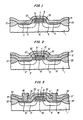
- Fig. 1 Depicted in Fig. 1 are substrate 1, a transistor having source and drain regions 3 and 5, respectively, a gate structure 7, and dielectric glass layer 9. Substrate 1 may have an upper epitaxial layer, if desired.
- the gate has, as is well known, a doped polysilicon conductor 15 overlying a thin oxide 13. Silicide region 21 is on top of conductor 15. Spacers 23 and 25 are positioned on either side of gate 7. Field oxides 27 and 29 are positioned adjacent source and drain regions 3 and 5, respectively.
- the source and drain regions 3 and 5 include silicide regions 17 and 19, respectively.
- Silicide regions 17 and 19 may be eliminated, if desired.
- Silicide regions 7,17, and 19 are formed by techniques known to those skilled in the art. Briefly, a thin layer (typically several hundred Angstroms) of metal -- for example, titanium, tungsten, cobalt, or tantalum -- is blanket deposited. The layer is subjected to a rapid thermal annealing, typically, in a nitrogen atmosphere at a temperature of approximately 600 o C for a few minutes. During the annealing step a portion of the metal reacts with the underlying silicon material. Then, the unreacted metal is etched away. Finally, another rapid thermal annealing in nitrogren at approximately 900 o C for a minute or so completes the silicide formation.
- metal for example, titanium, tungsten, cobalt, or tantalum
- the invention is applicable to transistors with various source and drain doping profiles, including lightly doped drain (LDD) structures.
- LDD lightly doped drain
- the structure depicted, except for the dielectric layer 9, may be formed by well-known techniques which therefore need not be described in further detail.
- the dielectric layer 9 is formed from the decomposition of tetraethoxysilane ((Si(OC2H5)4, abbreviated TEOS)) which includes boron and phosphorus.
- TEOS tetraethoxysilane
- BPTEOS boron and phosphorus
- TEOS TEOS
- the expression, "depositing a layer of TEOS”, is generally understood by those skilled in the art to mean the deposition of a dielectric glass layer by decomposition of TEOS in a reactor.
- the resulting dielectric layer is an oxide of silicon which exhibits better step coverage than oxides deposited by other means.
- TEOS is comparatively safer to handle than, for example, silane.
- BPTEOS BPTEOS
- phosphorous and boron dopants may be obtained, for example, from trimethylphosphite, phosphine, trimethylborate, trimethylphosphate, triethylphosphite, or triethylphosphate.
- doped dielectric includes dielectrics with at least one dopant which promotes flow present in an amount of at least one percent by weight. Examples of such dopants are boron, phosphorous, germanium, and arsenic.
- boron and phosphorus are each present in amounts ranging from approximately 3.5 to 4.5 percent by weight. Amounts of either boron or phosphorus greater than 5.0 percent are undesirable because boric acid or PBO4 particulates may form. Amounts less than 3.5 percent are undesirable because the deposited dielectric will not flow properly during subsequent smoothing steps.
- the specified range for boron and phosphorus allows good flow without permitting too much thinning of the dielectric on hills and too much thickening of the dielectric in valleys.
- step coverage is measured as x/y, where x is the minimum thickness on the vertical wall and y is the maximum thickness on the top horizontal surface, BPTEOS has a step coverage of about 0.9, while TEOS and BPSG have step coverages of about 0.5 and 0.7, respectively.
- the BPTEOS dielectric glass just described flows adequately, i.e., flows sufficiently to form a locally smooth surface, when maintained at a temperature of approximately 800 o C 50 o C in nitrogen for a time between one half hour and two hours. It is also believed that the flow eliminates voids. The 800 o C temperature does not degrade the desirable properties of the underlying salicides.
- integrated circuit fabrication continues in a conventional and well-known manner with, for example, patterning of the dielectric 9 to expose the source and drain regions of the device.
- Fig. 2 illustrates another exemplary embodiment of the present invention. Depicted in Fig. 2 are substrate 1′, a transistor with source and drain regions 3′ and 5′, respectively, and a gate structure 7′.
- the gate has a conductor 15′ overlying a thin oxide 13′.
- Silicide region 21′ is on top of conductor 15′.
- Spacers 23′ and 25′ are positioned on either side of gate 7′.
- spacers 25′ and 23′ are not as tall as gate 7′. Consequently, gate 7′ has sharp corners, or edges, 50′ and 51′.
- the occurrence of sharp corners, such as 50′ and 51′ in Fig. 2 can be due to a variety of manufacturing problems, including over-etching of spacers 25′ and 23′ and growth of silicide region 21′ during its formation.
- Sharp corners or edges on gate structure 7′ may cause thinning, or pinholes, in the BPTEOS layer after it is flowed.
- the sharp corners or edges can cause high electric fields which may cause a breakdown of the BPTEOS layer if it is too thin near the corners or edges.
- Fig. 2 illustrates a solution to the aforementioned problem.
- a layer of TEOS 31′ is deposited prior to the deposition of BPTEOS layer 33′.
- Layer 33′ is doped with boron and phosphorous to promote subsequent flow. Each dopant is preferably present in amounts ranging from 3.5 to 4.5 percent by weight.
- the TEOS layer will not flow at the temperature used to flow the BPTEOS.
- the thickness of TEOS layer 31′ is typically at least 1000 ⁇ to combat the pinhole and breakdown problems.
- TEOS layer 31′ is 2000 ⁇ 500 ⁇
- the thickness of the BPTEOS layer 33′ is typically 3500 500 ⁇ TEOS layer 31′ covers corners 50′ and 51′, and helps to prevent thinning of BPTEOS layer 33′ after the 800 o C flow. Consequently, the chances of pinholes and breakdown are substantially diminished.
- the desirable properties of silicide regions 17′, 19′, and 21′ are preserved.
- Fig. 3 shows the device of Fig. 2 after layer 33′ has flowed and windows 70′ and 71′ have been opened in layers 31′ and 33′ above silicide regions 17′ and 19′, respectively.
- Metal contacts 80′ and 81′ have been deposited by standard techniques in windows 70′ and 71′ to contact silicide regions 17′ and 19′. A similar windowing and metal contacting is, of course, also performed in the structure of Fig. 1.
- Embodiments other than those specifically described are contemplated.
- silicides other than TiSi2 such as CoSi2 may be used.
- the inventive process illustrated here is, of course, applicable to both salicide and silicide structures, i.e., self-alignment of the silicide is not a prerequisite for application of the invention.
- the dielectric structure of the present invention is applicable to devices using substrates other than silicon, e.g., devices utilizing III-V substrates.
- the embodiments illustrated in Figs. 2-3 may use other flowable dielectrics for layer 33′ and other non-flowable dielectrics (or dielectrics which flow at a higher temperature than the flow temperature of layer 33′) for layer 31′.
Landscapes
- Electrodes Of Semiconductors (AREA)
- Internal Circuitry In Semiconductor Integrated Circuit Devices (AREA)
- Formation Of Insulating Films (AREA)
Applications Claiming Priority (2)
| Application Number | Priority Date | Filing Date | Title |
|---|---|---|---|
| US264481 | 1981-05-18 | ||
| US26448188A | 1988-10-28 | 1988-10-28 |
Publications (3)
| Publication Number | Publication Date |
|---|---|
| EP0366343A2 true EP0366343A2 (fr) | 1990-05-02 |
| EP0366343A3 EP0366343A3 (en) | 1990-08-29 |
| EP0366343B1 EP0366343B1 (fr) | 1996-03-20 |
Family
ID=23006256
Family Applications (1)
| Application Number | Title | Priority Date | Filing Date |
|---|---|---|---|
| EP89310697A Expired - Lifetime EP0366343B1 (fr) | 1988-10-28 | 1989-10-18 | Fabrication d'un circuit intégré, comprenant une méthode à faible température pour faire des structures en silicide |
Country Status (5)
| Country | Link |
|---|---|
| EP (1) | EP0366343B1 (fr) |
| JP (1) | JP2589829B2 (fr) |
| DE (1) | DE68926017T2 (fr) |
| ES (1) | ES2084603T3 (fr) |
| HK (1) | HK145996A (fr) |
Cited By (7)
| Publication number | Priority date | Publication date | Assignee | Title |
|---|---|---|---|---|
| EP0465044A3 (en) * | 1990-06-27 | 1992-03-25 | American Telephone And Telegraph Company | Method of etching for integrated circuits with planarized dielectric |
| US5214305A (en) * | 1990-08-28 | 1993-05-25 | United Microelectronics Corporation | Polycide gate MOSFET for integrated circuits |
| US5336640A (en) * | 1991-01-28 | 1994-08-09 | Kawasaki Steel Corporation | Method of manufacturing a semiconductor device having an insulating layer composed of a BPSG film and a plasma-CVD silicon nitride film |
| EP0601723A3 (fr) * | 1992-11-24 | 1995-05-17 | American Telephone & Telegraph | Procédé de fabrication de circuit intégré. |
| WO1998000863A1 (fr) * | 1996-07-01 | 1998-01-08 | Advanced Micro Devices, Inc. | Procede pour simplifier la fabrication d'un empilement de dielectriques intercouches |
| US6455420B1 (en) * | 1997-08-22 | 2002-09-24 | Sony Corporation | Method of forming a compound film of a semiconductor and a metal by self-alignment |
| US6462394B1 (en) | 1995-12-26 | 2002-10-08 | Micron Technology, Inc. | Device configured to avoid threshold voltage shift in a dielectric film |
Families Citing this family (2)
| Publication number | Priority date | Publication date | Assignee | Title |
|---|---|---|---|---|
| JPH0582781A (ja) * | 1991-09-24 | 1993-04-02 | Nec Yamagata Ltd | 半導体集積回路装置 |
| US7067442B1 (en) | 1995-12-26 | 2006-06-27 | Micron Technology, Inc. | Method to avoid threshold voltage shift in thicker dielectric films |
Family Cites Families (4)
| Publication number | Priority date | Publication date | Assignee | Title |
|---|---|---|---|---|
| JPS6081833A (ja) * | 1983-10-11 | 1985-05-09 | Nec Corp | 半導体装置 |
| JPS6225451A (ja) * | 1985-07-25 | 1987-02-03 | Toshiba Corp | 相補型半導体装置の製造方法 |
| US4743564A (en) * | 1984-12-28 | 1988-05-10 | Kabushiki Kaisha Toshiba | Method for manufacturing a complementary MOS type semiconductor device |
| JPS6337638A (ja) * | 1986-07-31 | 1988-02-18 | Fujitsu Ltd | 半導体装置の製造方法 |
-
1989
- 1989-10-18 DE DE68926017T patent/DE68926017T2/de not_active Expired - Fee Related
- 1989-10-18 EP EP89310697A patent/EP0366343B1/fr not_active Expired - Lifetime
- 1989-10-18 ES ES89310697T patent/ES2084603T3/es not_active Expired - Lifetime
- 1989-10-27 JP JP1278820A patent/JP2589829B2/ja not_active Expired - Fee Related
-
1996
- 1996-08-01 HK HK145996A patent/HK145996A/en not_active IP Right Cessation
Cited By (8)
| Publication number | Priority date | Publication date | Assignee | Title |
|---|---|---|---|---|
| EP0465044A3 (en) * | 1990-06-27 | 1992-03-25 | American Telephone And Telegraph Company | Method of etching for integrated circuits with planarized dielectric |
| US5214305A (en) * | 1990-08-28 | 1993-05-25 | United Microelectronics Corporation | Polycide gate MOSFET for integrated circuits |
| US5336640A (en) * | 1991-01-28 | 1994-08-09 | Kawasaki Steel Corporation | Method of manufacturing a semiconductor device having an insulating layer composed of a BPSG film and a plasma-CVD silicon nitride film |
| EP0601723A3 (fr) * | 1992-11-24 | 1995-05-17 | American Telephone & Telegraph | Procédé de fabrication de circuit intégré. |
| US6462394B1 (en) | 1995-12-26 | 2002-10-08 | Micron Technology, Inc. | Device configured to avoid threshold voltage shift in a dielectric film |
| WO1998000863A1 (fr) * | 1996-07-01 | 1998-01-08 | Advanced Micro Devices, Inc. | Procede pour simplifier la fabrication d'un empilement de dielectriques intercouches |
| US5795820A (en) * | 1996-07-01 | 1998-08-18 | Advanced Micro Devices | Method for simplifying the manufacture of an interlayer dielectric stack |
| US6455420B1 (en) * | 1997-08-22 | 2002-09-24 | Sony Corporation | Method of forming a compound film of a semiconductor and a metal by self-alignment |
Also Published As
| Publication number | Publication date |
|---|---|
| JPH02170555A (ja) | 1990-07-02 |
| HK145996A (en) | 1996-08-09 |
| ES2084603T3 (es) | 1996-05-16 |
| DE68926017D1 (de) | 1996-04-25 |
| EP0366343B1 (fr) | 1996-03-20 |
| DE68926017T2 (de) | 1996-08-22 |
| EP0366343A3 (en) | 1990-08-29 |
| JP2589829B2 (ja) | 1997-03-12 |
Similar Documents
| Publication | Publication Date | Title |
|---|---|---|
| US6940172B2 (en) | Chemical vapor deposition of titanium | |
| DE69032234T2 (de) | Halbleiteranordnung mit einem durch Verfliessen gefüllten Graben | |
| JP2825074B2 (ja) | 半導体装置の製造方法 | |
| US5198387A (en) | Method and apparatus for in-situ doping of deposited silicon | |
| EP0746027A2 (fr) | Composites multicouches de polysilicium/tungstène siliciure formés sur une structure de circuit intégré et son procédé de fabrication amélioré | |
| US5814545A (en) | Semiconductor device having a phosphorus doped PECVD film and a method of manufacture | |
| US6888252B2 (en) | Method of forming a conductive contact | |
| JP2528961B2 (ja) | Vlsi装置の抵抗領域に低抵抗接続を形成する方法 | |
| US6515351B2 (en) | Integrated circuit with borderless contacts | |
| US6696368B2 (en) | Titanium boronitride layer for high aspect ratio semiconductor devices | |
| US6791149B2 (en) | Diffusion barrier layer for semiconductor wafer fabrication | |
| EP0366343B1 (fr) | Fabrication d'un circuit intégré, comprenant une méthode à faible température pour faire des structures en silicide | |
| JPH10199881A (ja) | 半導体装置の製造方法 | |
| US6221760B1 (en) | Semiconductor device having a silicide structure | |
| US4380773A (en) | Self aligned aluminum polycrystalline silicon contact | |
| US5869406A (en) | Method for forming insulating layers between polysilicon layers | |
| US4433469A (en) | Method of forming a self aligned aluminum polycrystalline silicon line | |
| EP0429885B1 (fr) | Procédé du dopage in-situ du silicium déposé | |
| CN1159076A (zh) | 半导体器件的平整方法 | |
| JP3071268B2 (ja) | 半導体装置の製造方法 | |
| US6169026B1 (en) | Method for planarization of semiconductor device including pumping out dopants from planarization layer separately from flowing said layer | |
| JP2880892B2 (ja) | 半導体装置の製造方法 | |
| JP2000216383A (ja) | 半導体装置及びその製造方法 | |
| JPH09148572A (ja) | 半導体装置の製造方法及び半導体装置 | |
| JPH06275726A (ja) | 半導体装置の製造方法 |
Legal Events
| Date | Code | Title | Description |
|---|---|---|---|
| PUAI | Public reference made under article 153(3) epc to a published international application that has entered the european phase |
Free format text: ORIGINAL CODE: 0009012 |
|
| AK | Designated contracting states |
Kind code of ref document: A2 Designated state(s): DE ES FR GB IT NL |
|
| PUAL | Search report despatched |
Free format text: ORIGINAL CODE: 0009013 |
|
| AK | Designated contracting states |
Kind code of ref document: A3 Designated state(s): DE ES FR GB IT NL |
|
| 17P | Request for examination filed |
Effective date: 19901211 |
|
| 17Q | First examination report despatched |
Effective date: 19930405 |
|
| RAP3 | Party data changed (applicant data changed or rights of an application transferred) |
Owner name: AT&T CORP. |
|
| GRAH | Despatch of communication of intention to grant a patent |
Free format text: ORIGINAL CODE: EPIDOS IGRA |
|
| GRAA | (expected) grant |
Free format text: ORIGINAL CODE: 0009210 |
|
| AK | Designated contracting states |
Kind code of ref document: B1 Designated state(s): DE ES FR GB IT NL |
|
| ITF | It: translation for a ep patent filed | ||
| ET | Fr: translation filed | ||
| REF | Corresponds to: |
Ref document number: 68926017 Country of ref document: DE Date of ref document: 19960425 |
|
| REG | Reference to a national code |
Ref country code: ES Ref legal event code: FG2A Ref document number: 2084603 Country of ref document: ES Kind code of ref document: T3 |
|
| PLBE | No opposition filed within time limit |
Free format text: ORIGINAL CODE: 0009261 |
|
| STAA | Information on the status of an ep patent application or granted ep patent |
Free format text: STATUS: NO OPPOSITION FILED WITHIN TIME LIMIT |
|
| 26N | No opposition filed | ||
| REG | Reference to a national code |
Ref country code: GB Ref legal event code: IF02 |
|
| PGFP | Annual fee paid to national office [announced via postgrant information from national office to epo] |
Ref country code: FR Payment date: 20020923 Year of fee payment: 14 |
|
| PGFP | Annual fee paid to national office [announced via postgrant information from national office to epo] |
Ref country code: GB Payment date: 20020926 Year of fee payment: 14 |
|
| PGFP | Annual fee paid to national office [announced via postgrant information from national office to epo] |
Ref country code: NL Payment date: 20021003 Year of fee payment: 14 |
|
| PGFP | Annual fee paid to national office [announced via postgrant information from national office to epo] |
Ref country code: ES Payment date: 20021029 Year of fee payment: 14 |
|
| PGFP | Annual fee paid to national office [announced via postgrant information from national office to epo] |
Ref country code: DE Payment date: 20021205 Year of fee payment: 14 |
|
| PG25 | Lapsed in a contracting state [announced via postgrant information from national office to epo] |
Ref country code: GB Free format text: LAPSE BECAUSE OF NON-PAYMENT OF DUE FEES Effective date: 20031018 |
|
| PG25 | Lapsed in a contracting state [announced via postgrant information from national office to epo] |
Ref country code: ES Free format text: LAPSE BECAUSE OF NON-PAYMENT OF DUE FEES Effective date: 20031020 |
|
| PG25 | Lapsed in a contracting state [announced via postgrant information from national office to epo] |
Ref country code: NL Free format text: LAPSE BECAUSE OF NON-PAYMENT OF DUE FEES Effective date: 20040501 Ref country code: DE Free format text: LAPSE BECAUSE OF NON-PAYMENT OF DUE FEES Effective date: 20040501 |
|
| GBPC | Gb: european patent ceased through non-payment of renewal fee |
Effective date: 20031018 |
|
| PG25 | Lapsed in a contracting state [announced via postgrant information from national office to epo] |
Ref country code: FR Free format text: LAPSE BECAUSE OF NON-PAYMENT OF DUE FEES Effective date: 20040630 |
|
| NLV4 | Nl: lapsed or anulled due to non-payment of the annual fee |
Effective date: 20040501 |
|
| REG | Reference to a national code |
Ref country code: FR Ref legal event code: ST |
|
| REG | Reference to a national code |
Ref country code: ES Ref legal event code: FD2A Effective date: 20031020 |
|
| PG25 | Lapsed in a contracting state [announced via postgrant information from national office to epo] |
Ref country code: IT Free format text: LAPSE BECAUSE OF NON-PAYMENT OF DUE FEES;WARNING: LAPSES OF ITALIAN PATENTS WITH EFFECTIVE DATE BEFORE 2007 MAY HAVE OCCURRED AT ANY TIME BEFORE 2007. THE CORRECT EFFECTIVE DATE MAY BE DIFFERENT FROM THE ONE RECORDED. Effective date: 20051018 |