EP0366265B1 - Phase detector for amplitude modulated radio frequency signals containing a low frequency waveform - Google Patents
Phase detector for amplitude modulated radio frequency signals containing a low frequency waveform Download PDFInfo
- Publication number
- EP0366265B1 EP0366265B1 EP89309687A EP89309687A EP0366265B1 EP 0366265 B1 EP0366265 B1 EP 0366265B1 EP 89309687 A EP89309687 A EP 89309687A EP 89309687 A EP89309687 A EP 89309687A EP 0366265 B1 EP0366265 B1 EP 0366265B1
- Authority
- EP
- European Patent Office
- Prior art keywords
- signal
- radio frequency
- amplitude
- detector
- output
- Prior art date
- Legal status (The legal status is an assumption and is not a legal conclusion. Google has not performed a legal analysis and makes no representation as to the accuracy of the status listed.)
- Expired - Lifetime
Links
- 239000003990 capacitor Substances 0.000 claims description 28
- 239000004020 conductor Substances 0.000 claims description 14
- 230000005540 biological transmission Effects 0.000 claims description 12
- 239000004065 semiconductor Substances 0.000 claims description 5
- 230000000694 effects Effects 0.000 claims description 4
- 230000008878 coupling Effects 0.000 claims description 2
- 238000010168 coupling process Methods 0.000 claims description 2
- 238000005859 coupling reaction Methods 0.000 claims description 2
- 230000001939 inductive effect Effects 0.000 claims 1
- 238000006243 chemical reaction Methods 0.000 description 24
- 230000006870 function Effects 0.000 description 14
- 238000010586 diagram Methods 0.000 description 8
- 238000004804 winding Methods 0.000 description 6
- 238000013461 design Methods 0.000 description 4
- 238000001914 filtration Methods 0.000 description 3
- 238000007667 floating Methods 0.000 description 3
- 238000010276 construction Methods 0.000 description 2
- 230000006872 improvement Effects 0.000 description 2
- 238000013459 approach Methods 0.000 description 1
- 230000008901 benefit Effects 0.000 description 1
- 230000008859 change Effects 0.000 description 1
- 238000012937 correction Methods 0.000 description 1
- 238000001514 detection method Methods 0.000 description 1
- 238000005259 measurement Methods 0.000 description 1
- 238000000034 method Methods 0.000 description 1
- 238000012986 modification Methods 0.000 description 1
- 230000004048 modification Effects 0.000 description 1
- 238000010587 phase diagram Methods 0.000 description 1
- 230000010363 phase shift Effects 0.000 description 1
- 230000001131 transforming effect Effects 0.000 description 1
Images


Classifications
-
- H—ELECTRICITY
- H03—ELECTRONIC CIRCUITRY
- H03D—DEMODULATION OR TRANSFERENCE OF MODULATION FROM ONE CARRIER TO ANOTHER
- H03D13/00—Circuits for comparing the phase or frequency of two mutually-independent oscillations
Definitions
- This disclosure relates to phase detectors for radio frequency circuit measurements.
- the most common radio frequency (RF) phase detector is a double balanced mixer.
- a double balanced mixer has a radio frequency (RF) port, a local oscillator (LO) port and an intermediate frequency (IF) port. The impedance of these three ports is 50 ohms.
- the mixer produces both a sum and a difference product. The sum product is removed by filtering so that only the difference product remains.
- the difference product for an ideal mixer is a cosine of the phase difference of the LO and RF frequencies.
- the phase slope of the mixer is a function of the IF power output. Because the derivative of a cosine wave is a sine wave, the peak voltage of the sinusoid is equal to the phase slope (volts/radian) when the output is at zero volts. For example, zero dBm at the IF output of the mixer is equal to a .316 volt peak sinewave into 50 ohms, and the phase slope is .316 volts per radian at zero volts output.
- the IF power at the output is a function of the RF and LO power at the input and the conversion loss of the mixer.
- Conversion loss is the difference between the RF power and the IF power.
- the LO power is much greater than the RF power, which gives the minimum conversion loss.
- the typical conversion loss of a mixer will vary between 6 and 9 dB. 3dB of the conversion loss is due to the lost power in the sum product that is filtered.
- the extra conversion loss is due to losses in the mixer and efficiency of the switching diodes. Increasing the RF power until it is equal to the LO power will increase the IF power and phase slope but at a lower conversion loss.
- phase slope K ⁇
- IF source resistance R i
- RF peak voltage V r
- RF source resistance R r
- the conversion loss is: (10)Log(V r 2/R r ) - (10)Log(K ⁇ 2 /R i ) Because K ⁇ equals the peak IF voltage for a cosine IF output, this definition is consistent with the case where the RF power is much less than the LO power.
- the conversion loss for mixers where the RF and the LO power levels are equal is typically 12 to 15 dB.
- a typical high level mixer with +20 dBm power into the RF and LO ports would have a peak RF voltage of 3.16 volts and a phase slope of .56 to .8 volts per radian.
- the noise floor of the phase detector can be determined.
- the source voltage is double the voltage measured when terminated into a 50 ohm load resistor because of the divide ratio of the source resistance and the load resistance.
- the single sideband phase noise of the phase detector referred back to the RF and LO source is equal to: (10)Log(.5(E n /K ⁇ )2), where E n is the IF source resistance noise.
- a typical mixer with a K ⁇ of .5 volts per radian terminated in 50 ohms would have a source voltage of 1 volt per radian and a source noise of .89 nanovolts, giving a single sideband phase noise floor of -184 dBc in a 1 Hz bandwidth.
- the noise figure of the phase detector is 3 dB less than the conversion loss of the phase detector as defined above.
- a conversion loss of 14 dB and a RF power of 18 dBm would give the .5 volts per radian discussed.
- the reason that the noise figure of the phase detector is 3 dB better than the conversion loss is that the double sideband noise at the RF port is converted to single sideband noise at the IF port. When relating single sideband noise at the IF port back to single sideband noise at the RF port, there is a 3 dB correction factor.
- the amplifier that follows the phase detector will also contribute to the noise floor of the phase detector. Its contribution can be accounted for in terms of noise figure.
- the noise figure of a typical differential pair amplifier is about 3 dB for a 50 ohm source impedance.
- the total noise floor of the phase detector and amplifier following the phase detector will be -181 dBc in a 1 Hz bandwidth giving a total noise figure of 14 dB.
- phase detector can be described as a sum-difference peak detector. This detector adds the RF to the LO at one output port and subtracts the RF from the LO at the other output port. By peak detecting the signals at the sum port and difference port and subtracting the outputs of the peak detectors, a very high phase slope for relatively low RF and LO powers is achieved.
- the source impedance of a peak detector can be very high. Given the definition of the conversion loss of the phase detector, a very high phase slope could have a very poor conversion loss if the IF source impedance is very high. For example, using a peak detector on the sum and difference ports would give an IF voltage output of equal to twice the RF voltage input. With a source impedance of about 10000 ohms, the conversion loss would be 17 dB. This high a conversion loss makes the phase detector undesirable for low noise applications.
- phase comparator adapted to provide so called ambiguous and non-ambiguous phase comparison of two inputs and to make the results of the comparisons available each at one or other of the two output terminals comprising four four-port quarter wave directional coupling devices, two being termed input devices and two being termed output devices, and each device having two diagonally opposite input ports and two diagonally opposite output ports; interconnections connecting the four devices in a ring sequence such that the output ports of the said input devices are connected in ring sequence to the input ports of the said output devices; a 90° phase shifter included in one of said connections; means for applying one input to one of the remaining input ports of one of said input devices; means for applying the other input to one of the remaining input ports of the second input device which is separated from said one input device in the ring sequence by the two output devices; means for rectifying the vector sum of two signals appearing at a remaining output port of one of the said two output devices to produce a non
- the invention provides a low noise floor phase detector for radio frequency signals, comprising radio frequency signal combining means having two signal inputs for respectively receiving incoming signals from two radio frequency sources and having two signal outputs, the amplitudes of the radio frequency signals at each signal output being summations of the two incoming signals and the phase angle of at least one of the incoming signals being shifted by a constant angular amount between the two signal outputs; a pair of amplitude detectors respectively connected to the signal outputs of the combining means, each amplitude detector comprising:
- the invention provides a low noise floor phase detector for radio frequency signals, comprising radio frequency signal combining means having two signal inputs for respectively receiving incoming signals from two radio frequency sources and having two signal outputs, the amplitudes of the radio frequency signals at each signal output being summations of the two incoming signals and the phase angle of at least one of the incoming signals being shifted by a constant angular amount between the two signal outputs; a pair of amplitude detectors respectively connected to the signal outputs of the combining means, each amplitude detector comprising:
- This invention is a low noise phase detector as illustrated generally in Figs. 1A and 1B.
- the phase detector consists of a means 10 for combining two radio frequency (RF) signals, and a high signal to noise ratio (SNR) means 11 for detecting the amplitudes of the combined RF signals.
- the means 10 for combining the two RF signals consists of two RF inputs (ports A and B) and two RF outputs (ports C and D) such that the signals at the outputs are equal linear summations of the inputs. For example, an RF signal applied at A by a radio frequency (RF) source 12 will result in equal signal levels at C and D. Also an RF signal applied at B by a reference local oscillator source 13 will result in equal signal levels at C and D.
- RF radio frequency
- phase relationship at the outputs should be such that when the two RF signals from A and B arrive in phase at port C they are 180 degrees out of phase at port D - when the phase is +90 degrees at port C it is -90 degrees at port D, when the phase is 180 degrees at port C it is zero degrees at port D.
- the amplitude at port C will increase as the relative phase between the signals from port A and port B changes from 180 degrees to zero degrees. The same is true for port D.
- the phase difference at C is 90 degrees (plus or minus) and 90 degrees (plus or minus) at port D
- the amplitude at port C and D will be the same.
- the high SNR amplitude detectors at ports C and D measure the amplitude of the combined RF signals from ports A and B. Subtracting the outputs of the two amplitude detectors gives a phase detector output which varies with the relative phase of the RF signal at port A and the RF signal at port B.
- the phase slope of this phase detector is a function of the amplitude detector constant and the loss of the device that combines the RF signals.
- the source impedance is twice the source impedance of one of the amplitude detectors, since they are used in series.
- a combining means 10 would be a 3 dB transmission line coupler (Fig. 1A).
- the phase relationship between the signal output at the coupled port and the thru port is always 90 degrees for any transmission line coupler. This meets the necessary conditions as stated above.
- the RF source impedance at the outputs C and D is 50 ohms for a 50 ohm coupler.
- the detector source impedance for each of the low noise AM detectors can be designed to be approximately 300 ohms. The total source impedance is therefore 600 ohms.
- the phaselope for this detector is 2.2 times the peak RF source voltage when the LO power level is much larger than the RF power level. This gives a conversion loss of 4 dB.
- the conversion loss is only 3 dB higher, bringing the conversion loss to 7 dB.
- the typical loss of a transmission line coupler is less than 1 dB, giving a worst case conversion loss of 8 dB.
- the conversion loss is about 4 to 7 dB better than the example of the mixer as a phase detector discussed in the background information of this disclosure.
- the same low noise amplifier would have a .4 db noise figure compared to a 3 db noise figure in a 50 ohm system. This gives a total improvement of 6 to 9 dB over the mixer method.
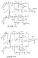
- Figs. 1A and 1B illustrate the general circuitry of the phase detector.
- the combining means 10 for the two incoming RF signals in Fig. 1A is a transmission line coupler 50. This might be a pair of parallel traces on a circuitboard or a pair of conductive wires.
- the transmission line coupler is a 3 dB coupler of known construction, comprising a length of coaxial cable having a pair of twisted interior conductors insulated from one another and located within a surrounding shield.
- the combining means is shown as a conventional 2:1 transformer 51.
- the combining means 10 has two signal inputs designated by the letters A and B, and two signal outputs, designated by letters C and D.
- the signal outputs C and D serve as both through ports and coupled ports for the incoming radio frequency signals from signal inputs A and B. More specifically, in Fig. 1A the signal output C is a through port for the RF signal from signal input B and a coupled port for the RF signal at signal input A. Signal output D is operatively connected to the signal inputs A and B in an opposite manner. In Fig. 1B, signal outputs C and D are through ports for the RF signal at signal input B and coupled ports for the RF signal at signal input A.
- the amplitudes of the radio RF at each signal outputs C and D are summations of the two incoming RF signals at signal inputs A and B.
- the phase angle of at least one of the incoming signals at signal inputs A or B must be shifted by a constant angular amount between the two signal outputs C and D.
- the phase of each signal input is shifted 90 degrees between the two signal outputs C and D.
- the transformer 51 shown in Fig. 1B the phase of the incoming signal from signal input A is shifted 180 degrees between signal outputs C and D, and no phase shift occurs with respect to the incoming signal from signal input B.
- the signal outputs C and D are connected to separate upper and lower amplitude detectors 11A and 11B, respectively, each including a pair of diodes 21, 31 and signal terminating means 26, illustrated in Figs. 1A and 1B as a constant current source 26.
- Fig. 1A for example, in amplitude detector 11A one side of diode 21 is connected to ground through a capacitor 22, and the corresponding side of diode 31 is connected to ground through capacitor 24 and the LO signal source 13.
- the lower amplitude detector 11B the same circuitry is used, with the one side of its diode 31 being connected to ground through an identical capacitor 24 and the RF signal source 12.
- the signal sources 12 and 13 can be separate sources, but will typically be a single source of RF signals having the signal divided through a delay line or a circuit loop that will effect a constant phase relationship between the two signals directed to the phase detector.
- the demodulated output signals from the amplitude detectors are directed to summation means shown in Figs. 1A and 1B as amplifier 54.
- the output of amplifier 54 is a function of the differences between the demodulated output voltages of the two amplitude detectors.
- Fig. 2 generally illustrates the components and circuit equivalents included within the amplitude detector.
- a pair of semi-conductor diodes 21, 31 are oriented oppositely to one another within parallel circuits adapted to be operatively connected to a radio frequency (RF) signal source 20.
- RF radio frequency
- a first capacitor 22 is operatively connected between one side of the first diode 21 and ground.
- a second capacitor 32 is operatively connected between one side of the second diode 31 and ground.
- the amplitude detector is completed by terminating means 23 connected across the parallel circuits for properly biasing each diode to cause it to conduct current from the signal source 20 at a conduction angle ⁇ , which is graphically illustrated in Fig. 3.
- the conduction angle is selected to minimize the Signal to Noise Ratio (SNR) of the amplitude detector. It also matches the radio frequency load impedance of the amplitude detector to the radio frequency impedance of the signal source 20.
- the signal terminating means 23 has an output at which a demodulated signal is produced having an amplitude proportional to the amplitude of any low frequency signal present in a radio frequency signal directed to the amplitude detector from the signal source 20.
- the waveform of a typical RF signal having a sinusoidal shape can be expressed by the formula V p Cos ⁇ t, where V p is the peak voltage amplitude of the incoming RF signal.
- R s denotes the RF impedance of signal source 20, which is conventionally 50 ohms.
- the inclusion of capacitor 24 in conjunction with capacitors 22 and 32 is a circuit design alternative that is described below.
- R d is a circuit equivalent for the typical dynamic on resistance of each diode 21, 31. For illustration, R d is quantified as 10 ohms.
- the inductor 25 provides RF filtering of the low frequency signal prior to the signal terminating means 23.
- Signal terminating means 23 is illustrated as two separate devices leading from each parallel circuit to ground. The current flowing through each device is designated as I dc .
- the voltage level at the connection between the signal terminating means 23 and each parallel circuit is designated as V dc .
- the output voltage across the terminal ends of the parallel circuits is designated as V out and is equal to 2V dc .
- Fig. 3 graphically illustrates the angular relationships between voltage and current (indicated by the shaded lines within the sinusoidal curve) for a selected diode conduction angle ⁇ .
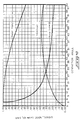
- the calculation of ⁇ and the radio frequency load impedance of the amplitude detector (R in ) is presented in Fig. 6. It can be seen that when these mathematical relationships are solved to determine the maximum Signal to Noise Ratio, ⁇ equals 1.165 radians or approximately 67°. This means that each diode 21, 22 conducts over a total angle of 134° during each half cycle of the incoming radio frequency waves or during 37% of each full cycle. Once the optimum conduction angle for lowest noise operation is determined, one can calculate the low frequency source impedance of the amplitude detector required to achieve optimal operation.
- the amplitude detector source impedance is 2.695 times the impedance of the RF source impedance, which in turn is the sum of the impedance of source 20 plus the impedance of each diode 21, 31 (R s plus R d ).
- the average RF load impedance that the amplitude detector presents to the RF source 20 is approximately equal to the source impedance of the RF source. This properly matches the radio frequency load impedance of the detector to the radio frequency impedance of the signal source for efficient termination of the RF signal.
- Figs. 4 and 5 are plots of theoretically derived data relating to the Signal to Noise Ratio as a function of diode conduction angle (Fig. 4) and the conduction angle as a function of the dynamic source impedance of the detector, as well as a passive resistor load utilized as the signal terminating means 23. They graphically illustrate the optimum Signal to Noise Ratio and load matching that occur at a conduction angle of 67°.
- Figs. 8 - 10 schematically illustrate variations in circuit design that incorporate the operational features described above.
- three capacitors are used, the third capacitor 24 providing a "floating" RF signal input to the parallel circuits that include diodes 21, 31.
- Fig. 9 only two capacitors are used.
- One diode 31 has one side shorted directly to ground and its remaining side is connected to ground through the floating connection provided by capacitor 24 and the signal source 20. It is to be understood that either diode 21 or 31 can have one side directly shorted to ground in this manner.
- Fig. 10 shows the use of both capacitors 22, 32 as previously described, with one side of diode 31 shunted to ground directly through the RF signal source 20.
- Figs. 11 through 14 schematically illustrate the various types of devices that can be used as the terminating means 23 in the amplitude detector.
- Figs. 11 and 12 numerically indicate the low frequency impedance value of the terminating means 23 required to achieve the selected diode conduction angle of 67°. It is stated as a function of the signal source impedance R s .
- the terminating means is shown as a constant current source 26, the output, (V out ), being the voltage across the current source 26.
- the output voltage may be measured by a conventional voltage meter 14 connected across the current source 26.
- the signal terminating means is a constant voltage source 27 and the output of the amplitude detector (I out ) is readable as the current flowing through voltage source 27.
- the output current signal may be measured by a conventional current meter 15 in series with the voltage source 27.
- the signal terminating means is a passive resistive load or resistor 28 and the output (V out ) is readable as the voltage across resistor 28.
- the signal terminating means is a active resistive load comprising amplifier 29 and feedback resistor 30 where the value of resistor 30 is given by the equation shown and provides an equivalent impedance equal to that shown in Fig. 13.
- the output is readable as changes in the voltage output (V out ) at the output terminals of amplifier 29.
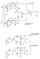
- FIG. 7 A simplified circuit diagram of the current phase detector circuitry is shown in Fig. 7.
- two incoming radio frequency signals are fed to the radio frequency (RF) and local oscillator (LO) signal inputs of a combining means 40 having separate signal outputs 41 and 42.
- Signal outputs 41 and 42 serve as both through ports and coupled ports for the incoming radio frequency signals at the signal inputs.
- the phase angle of at least one of the incoming signals is shifted by a constant angular amount between the two signal outputs 41 and 42.
- the combining means 40 might be a transformer, it is preferably a transmission line coupler, such as a length of coaxial cable having a pair of twisted interior conductors insulated from one another and surrounded by a cylindrical shield.
- Each signal output 41, 42 is fed to an amplitude detector 43 of the type described above.
- the two diodes 21, 31, which are included within parallel circuits from the signal outputs 41, 42, are connected with one side of diode 21 shunted to ground through capacitor 22 and one side of diode 31 shunted to ground. Filtering of RF wave forms is assured through provision of a filter comprised of an inductor 44 and capacitor 45.
- the signal terminating means 23 is shown in Fig. 7 as passive resistors 47.
- a constant voltage source 46 in series with each resistor 47 provides the turn on voltage for the diodes of the amplitude detectors.
- the output signals from the two amplitude detectors are directed to a summation means that produces a signal that is a function of any difference in the amplitudes of the demodulated signals produced by the amplitude detectors 43.
- the illustrated summation means is an operational amplifier 48 and a resistor 49 that provides negative feedback. Any differences in the output voltage amplitudes at the amplitude detectors 43 will be reflected as a change in voltage (V a ) at the output of operational amplifier 48.
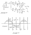
- Fig. 15 relates the RF signal at the signal outputs C and D of a transmission line coupler 50 to the respective phase characteristics of the incoming LO and RF signals. These phase relationships at signal outputs C and D are illustrated by vector diagrams 16A and 16B. It is assumed for purposes of Figs. 16A and 16B, that the signals at signal outputs C and D have equal amplitudes and that the phase angles of the LO and RF incoming signals are identical. It can be seen that as the phase of the LO signal increases relative to that of the RF signal, the amplitude of the signal at C will increase and the amplitude of the signal at D will decrease until the phase angle between the signals at A and B is 90 degrees relative to each other. Similarly, Figs.
- the noise improvement of this invention is about 6 to 9 dB when compared to the mixer used as a phase detector.
- This invention has the effect of transforming the 50 ohm source impedance up to a 600 ohm source impedance with a corresponding increase in phase slope. This makes the design of the phase detector amplifier much easier because less gain is required and low noise figure is easy to achieve.
- phase slope will increase linearly with increasing power, limited only by the power dissipation of the diodes.
- higher phase slope is achieved by placing diodes in series for higher LO drive levels, causing higher conversion loss.
- phase detector at very low RF power levels into both ports. By biasing the amplitude detector diodes at their turn on voltage, they are able to amplitude detect low power levels.
Landscapes
- Engineering & Computer Science (AREA)
- Power Engineering (AREA)
- Measurement Of Resistance Or Impedance (AREA)
- Monitoring And Testing Of Transmission In General (AREA)
- Radar Systems Or Details Thereof (AREA)
- Transmitters (AREA)
Description
- This disclosure relates to phase detectors for radio frequency circuit measurements.
- The most common radio frequency (RF) phase detector is a double balanced mixer. A double balanced mixer has a radio frequency (RF) port, a local oscillator (LO) port and an intermediate frequency (IF) port. The impedance of these three ports is 50 ohms. The mixer produces both a sum and a difference product. The sum product is removed by filtering so that only the difference product remains. The difference product for an ideal mixer is a cosine of the phase difference of the LO and RF frequencies. The phase slope of the mixer is a function of the IF power output. Because the derivative of a cosine wave is a sine wave, the peak voltage of the sinusoid is equal to the phase slope (volts/radian) when the output is at zero volts. For example, zero dBm at the IF output of the mixer is equal to a .316 volt peak sinewave into 50 ohms, and the phase slope is .316 volts per radian at zero volts output.
- The IF power at the output is a function of the RF and LO power at the input and the conversion loss of the mixer. Conversion loss is the difference between the RF power and the IF power. Usually the LO power is much greater than the RF power, which gives the minimum conversion loss. The typical conversion loss of a mixer will vary between 6 and 9 dB. 3dB of the conversion loss is due to the lost power in the sum product that is filtered. The extra conversion loss is due to losses in the mixer and efficiency of the switching diodes. Increasing the RF power until it is equal to the LO power will increase the IF power and phase slope but at a lower conversion loss.
- With equal power at the LO and RF ports, the output approaches a triangle wave instead of a cosine wave. In order to maintain a consistent definition of conversion loss of a phase detector, it can be redefined in terms of phase slope, IF port source resistance, RF power and RF source resistance. Let phase slope equal Kφ, IF source resistance equal Ri, RF peak voltage equal Vr, and RF source resistance equal Rr. The conversion loss is:

Because Kφ equals the peak IF voltage for a cosine IF output, this definition is consistent with the case where the RF power is much less than the LO power. The conversion loss for mixers where the RF and the LO power levels are equal is typically 12 to 15 dB. For example, a typical high level mixer with +20 dBm power into the RF and LO ports would have a peak RF voltage of 3.16 volts and a phase slope of .56 to .8 volts per radian. - By modeling the IF output of the mixer as a ideal voltage source and a 50 ohm source resistance, the noise floor of the phase detector can be determined. The source voltage is double the voltage measured when terminated into a 50 ohm load resistor because of the divide ratio of the source resistance and the load resistance. The single sideband phase noise of the phase detector referred back to the RF and LO source is equal to:

where En is the IF source resistance noise. Therefore, a typical mixer with a Kφ of .5 volts per radian terminated in 50 ohms would have a source voltage of 1 volt per radian and a source noise of .89 nanovolts, giving a single sideband phase noise floor of -184 dBc in a 1 Hz bandwidth. - The noise figure of the phase detector is 3 dB less than the conversion loss of the phase detector as defined above. For the above example, a conversion loss of 14 dB and a RF power of 18 dBm would give the .5 volts per radian discussed. 18 dBm of RF power has a single sideband phase noise floor of -177-18 = -195 dBc. The noise figure is -184-(-195) = 11 dB. This result is 3 dB less than the 14 dB of conversion loss. The reason that the noise figure of the phase detector is 3 dB better than the conversion loss is that the double sideband noise at the RF port is converted to single sideband noise at the IF port. When relating single sideband noise at the IF port back to single sideband noise at the RF port, there is a 3 dB correction factor.
- The amplifier that follows the phase detector will also contribute to the noise floor of the phase detector. Its contribution can be accounted for in terms of noise figure. The noise figure of a typical differential pair amplifier is about 3 dB for a 50 ohm source impedance. For the example above the total noise floor of the phase detector and amplifier following the phase detector will be -181 dBc in a 1 Hz bandwidth giving a total noise figure of 14 dB.
- Another type of phase detector can be described as a sum-difference peak detector. This detector adds the RF to the LO at one output port and subtracts the RF from the LO at the other output port. By peak detecting the signals at the sum port and difference port and subtracting the outputs of the peak detectors, a very high phase slope for relatively low RF and LO powers is achieved. However, the source impedance of a peak detector can be very high. Given the definition of the conversion loss of the phase detector, a very high phase slope could have a very poor conversion loss if the IF source impedance is very high. For example, using a peak detector on the sum and difference ports would give an IF voltage output of equal to twice the RF voltage input. With a source impedance of about 10000 ohms, the conversion loss would be 17 dB. This high a conversion loss makes the phase detector undesirable for low noise applications.
- Reference is made to DE-A-1949402 and to GB-A-1236829. These describe a phase comparator adapted to provide so called ambiguous and non-ambiguous phase comparison of two inputs and to make the results of the comparisons available each at one or other of the two output terminals comprising four four-port quarter wave directional coupling devices, two being termed input devices and two being termed output devices, and each device having two diagonally opposite input ports and two diagonally opposite output ports; interconnections connecting the four devices in a ring sequence such that the output ports of the said input devices are connected in ring sequence to the input ports of the said output devices; a 90° phase shifter included in one of said connections; means for applying one input to one of the remaining input ports of one of said input devices; means for applying the other input to one of the remaining input ports of the second input device which is separated from said one input device in the ring sequence by the two output devices; means for rectifying the vector sum of two signals appearing at a remaining output port of one of the said two output devices to produce a non-ambiguous output; means for rectifying the vector sum of two signals appearing at an output port of said other of said two output devices to produce a D.C. voltage of one polarity; means for rectifying the vector sum of two signals appearing at the remaining output port of said other of said two output devices to produce a D.C. voltage of the opposite polarity; means for algebraically adding the two D.C. voltages to produce an ambiguous output.
- Reference is also made to US-A-3634767 which describes a switching-modulation detector circuit, adapted for receiving amplitude-modulation signals generated in a switching comparison high-frequency radiometer system, comprising: transformer means having first and second coupled windings; input means connected across said first winding; first, second, and third conductor means, said first and second conductor means being connected to said second winding; said third conductor means being connected to said first winding; said first and third conductor means being adapted to serve as output means; first and second diode means; said first diode means being serially connected within said first conductor means; said second diode means being connected to said first conductor means between said first diode means and said second winding and to said third conductor means; first and second capacitor means; said first capacitor means being connected to said first conductor means on the side of said first diode means remote from said second winding and to said second conductor means; said second capacitor means being connected to said second and third conductor means adjacent said first capacitor means; first and second resistor means respectively connected in shunt across said first and second capacitor means, and adjustable unidirectional bias current source means connected to said first and third conductor means; said first and second diode means being so poled and so coupled to said condenser means and said resistor means as to remove said amplitude modulation signal from said amplitude-modulated signal for supply to said output means; said bias source means being so cooperatively arranged and connected as to supply bias current in series relation through a said first and second diode means for improving the efficiency of operation thereof.
- Further reference is made to DE-A-1200941 which describes a phase discriminator.
- In a first aspect, the invention provides a low noise floor phase detector for radio frequency signals, comprising
radio frequency signal combining means having two signal inputs for respectively receiving incoming signals from two radio frequency sources and having two signal outputs, the amplitudes of the radio frequency signals at each signal output being summations of the two incoming signals and the phase angle of at least one of the incoming signals being shifted by a constant angular amount between the two signal outputs;
a pair of amplitude detectors respectively connected to the signal outputs of the combining means, each amplitude detector comprising: - 1) a pair of semiconductor diodes oriented oppositely to one another within circuits coupled in parallel to one signal output of the combining means;
- 2) a first capacitor coupled between one side of one diode and ground;
- 3) a second capacitor coupled between one side of the remaining diode and ground; and
- 4) terminating means coupled across the parallel circuits for biasing each diode at a predetermined conduction angle causing the individual diodes to conduct in sequence during a predetermined percent of each radio frequency signal cycle for optimum signal-to-noise ratio of the amplitude detector while matching the radio frequency load impedance of the amplitude detector to the radio frequency impedance of the one signal output, the signal terminating means providing an output which is a demodulated signal having an amplitude proportional to the amplitude of any low frequency signal present in a radio frequency signal at the one signal output of the combining means;
- In a further aspect, the invention provides a low noise floor phase detector for radio frequency signals, comprising
radio frequency signal combining means having two signal inputs for respectively receiving incoming signals from two radio frequency sources and having two signal outputs, the amplitudes of the radio frequency signals at each signal output being summations of the two incoming signals and the phase angle of at least one of the incoming signals being shifted by a constant angular amount between the two signal outputs;
a pair of amplitude detectors respectively connected to the signal outputs of the combining means, each amplitude detector comprising: - 1) a pair of semiconductor diodes oriented oppositely to one another within circuits coupled in parallel to one signal output of the combining means;
- 2) a first capacitor coupled between one side of one diode and ground;
- 3) a second capacitor coupled between the parallel connection of the diodes and said one signal output of the combining means;
- 4) terminating means coupled across the parallel circuits for biasing each diode at a predetermined conduction angle causing the individual diodes to conduct in sequence during a predetermined percent of each radio frequency signal cycle for optimum signal-to-noise ratio of the amplitude detector while matching the radio frequency load impedance of the amplitude detector to the radio frequency impedance of the one signal output, the signal terminating means providing an output which is a demodulated signal having an amplitude proportional to the amplitude of any low frequency signal present in a radio frequency signal at the one signal output of the combining means;
-
- Fig. 1A is a simplified circuit diagram showing the general components of the phase detector;
- Fig. 1B is a modified version of the circuit in Fig. 1A;
- Fig. 2 is a schematic diagram illustrating the general circuit components of an amplitude detector constructed according to this disclosure;
- Fig. 3 is a graph of output voltage as a function of radians;
- Fig. 4 is a plot of SNR, noise and signal amplitude as a function of diode conduction angle;
- Fig. 5 is a plot of diode conduction angle as a function of the source impedance and load resistance (on a logarithmic scale);
- Fig. 6 is a summarized listing of the mathematical relationships by which the diode conduction angle for maximum SNR was calculated;
- Fig. 7 is a simplified wiring diagram of the present best mode for carrying out this invention;
- Figs 8-10 generally illustrate three variations of the amplitude detector circuitry; and
- Figs. 11-14 schematically illustrate four types of terminations usable in the amplitude detector;
- Fig. 15 is a schematic diagram of the transmission line coupler;
- Figs. 16A and 16B are phase vector diagrams illustrating signal components at outputs A and B, respectively in Fig. 15, when the incoming signals RF and LO are in phase; and
- Figs. 17A and 17B are phase vector diagrams illustrating the signal components at outputs C and D in Fig. 15 when the signals RF and LO are out of phase 180 degrees relative to each other.
- This invention is a low noise phase detector as illustrated generally in Figs. 1A and 1B. The phase detector consists of a
means 10 for combining two radio frequency (RF) signals, and a high signal to noise ratio (SNR) means 11 for detecting the amplitudes of the combined RF signals. The means 10 for combining the two RF signals consists of two RF inputs (ports A and B) and two RF outputs (ports C and D) such that the signals at the outputs are equal linear summations of the inputs. For example, an RF signal applied at A by a radio frequency (RF)source 12 will result in equal signal levels at C and D. Also an RF signal applied at B by a reference local oscillator source 13 will result in equal signal levels at C and D. Applying a signal at both inputs will result in a linear summation at the outputs. The phase relationship at the outputs should be such that when the two RF signals from A and B arrive in phase at port C they are 180 degrees out of phase at port D - when the phase is +90 degrees at port C it is -90 degrees at port D, when the phase is 180 degrees at port C it is zero degrees at port D. The amplitude at port C will increase as the relative phase between the signals from port A and port B changes from 180 degrees to zero degrees. The same is true for port D. When the phase difference at C is 90 degrees (plus or minus) and 90 degrees (plus or minus) at port D, the amplitude at port C and D will be the same. - The high SNR amplitude detectors at ports C and D measure the amplitude of the combined RF signals from ports A and B. Subtracting the outputs of the two amplitude detectors gives a phase detector output which varies with the relative phase of the RF signal at port A and the RF signal at port B. The phase slope of this phase detector is a function of the amplitude detector constant and the loss of the device that combines the RF signals. The source impedance is twice the source impedance of one of the amplitude detectors, since they are used in series.
- One example for a combining means 10 would be a 3 dB transmission line coupler (Fig. 1A). The phase relationship between the signal output at the coupled port and the thru port is always 90 degrees for any transmission line coupler. This meets the necessary conditions as stated above. The RF source impedance at the outputs C and D is 50 ohms for a 50 ohm coupler. The detector source impedance for each of the low noise AM detectors can be designed to be approximately 300 ohms. The total source impedance is therefore 600 ohms. For a lossless coupler, the phaselope for this detector is 2.2 times the peak RF source voltage when the LO power level is much larger than the RF power level. This gives a conversion loss of 4 dB. When the RF and LO signal inputs of the phase detector have equal power levels, the conversion loss is only 3 dB higher, bringing the conversion loss to 7 dB. The typical loss of a transmission line coupler is less than 1 dB, giving a worst case conversion loss of 8 dB. For this example, the conversion loss is about 4 to 7 dB better than the example of the mixer as a phase detector discussed in the background information of this disclosure. In a 600 ohm system, the same low noise amplifier would have a .4 db noise figure compared to a 3 db noise figure in a 50 ohm system. This gives a total improvement of 6 to 9 dB over the mixer method.
- Figs. 1A and 1B illustrate the general circuitry of the phase detector. The combining means 10 for the two incoming RF signals in Fig. 1A is a
transmission line coupler 50. This might be a pair of parallel traces on a circuitboard or a pair of conductive wires. In a preferred form of this invention, the transmission line coupler is a 3 dB coupler of known construction, comprising a length of coaxial cable having a pair of twisted interior conductors insulated from one another and located within a surrounding shield. In Fig. 1B, the combining means is shown as a conventional 2:1transformer 51. - In both Fig. 1A and 1B, the combining means 10 has two signal inputs designated by the letters A and B, and two signal outputs, designated by letters C and D. The signal outputs C and D serve as both through ports and coupled ports for the incoming radio frequency signals from signal inputs A and B. More specifically, in Fig. 1A the signal output C is a through port for the RF signal from signal input B and a coupled port for the RF signal at signal input A. Signal output D is operatively connected to the signal inputs A and B in an opposite manner. In Fig. 1B, signal outputs C and D are through ports for the RF signal at signal input B and coupled ports for the RF signal at signal input A.
- The amplitudes of the radio RF at each signal outputs C and D are summations of the two incoming RF signals at signal inputs A and B. To provide phase detection, the phase angle of at least one of the incoming signals at signal inputs A or B must be shifted by a constant angular amount between the two signal outputs C and D. In the case of a transmission line coupler 50 (Fig. 1A), the phase of each signal input is shifted 90 degrees between the two signal outputs C and D. In the case of the
transformer 51 shown in Fig. 1B, the phase of the incoming signal from signal input A is shifted 180 degrees between signal outputs C and D, and no phase shift occurs with respect to the incoming signal from signal input B. These phase relationships will be described further with respect to the phase diagrams shown in Figs. 16A, 16B, 17A and 17B. - The signal outputs C and D are connected to separate upper and lower amplitude detectors 11A and 11B, respectively, each including a pair of
diodes current source 26. In Fig. 1A, for example, in amplitude detector 11A one side ofdiode 21 is connected to ground through acapacitor 22, and the corresponding side ofdiode 31 is connected to ground throughcapacitor 24 and the LO signal source 13. In the lower amplitude detector 11B, the same circuitry is used, with the one side of itsdiode 31 being connected to ground through anidentical capacitor 24 and theRF signal source 12. It is to be understood that thesignal sources 12 and 13 can be separate sources, but will typically be a single source of RF signals having the signal divided through a delay line or a circuit loop that will effect a constant phase relationship between the two signals directed to the phase detector. - The demodulated output signals from the amplitude detectors are directed to summation means shown in Figs. 1A and 1B as
amplifier 54. The output ofamplifier 54 is a function of the differences between the demodulated output voltages of the two amplitude detectors. - Fig. 2 generally illustrates the components and circuit equivalents included within the amplitude detector. A pair of
semi-conductor diodes signal source 20. Afirst capacitor 22 is operatively connected between one side of thefirst diode 21 and ground. Asecond capacitor 32 is operatively connected between one side of thesecond diode 31 and ground. - The amplitude detector is completed by terminating
means 23 connected across the parallel circuits for properly biasing each diode to cause it to conduct current from thesignal source 20 at a conduction angle ϑ, which is graphically illustrated in Fig. 3. The conduction angle is selected to minimize the Signal to Noise Ratio (SNR) of the amplitude detector. It also matches the radio frequency load impedance of the amplitude detector to the radio frequency impedance of thesignal source 20. The signal terminating means 23 has an output at which a demodulated signal is produced having an amplitude proportional to the amplitude of any low frequency signal present in a radio frequency signal directed to the amplitude detector from thesignal source 20. - Referring further to Fig. 2, the waveform of a typical RF signal having a sinusoidal shape, can be expressed by the formula VpCos ωt, where Vp is the peak voltage amplitude of the incoming RF signal. Rs denotes the RF impedance of
signal source 20, which is conventionally 50 ohms.Capacitor 24, shown to be in series betweensignal source 20 and the two parallel diode circuits, provides a "floating" input signal relative to ground. The inclusion ofcapacitor 24 in conjunction withcapacitors diode inductor 25 provides RF filtering of the low frequency signal prior to thesignal terminating means 23. Signal terminating means 23 is illustrated as two separate devices leading from each parallel circuit to ground. The current flowing through each device is designated as Idc. The voltage level at the connection between the signal terminating means 23 and each parallel circuit is designated as Vdc. The output voltage across the terminal ends of the parallel circuits is designated as Vout and is equal to 2Vdc. - Fig. 3 graphically illustrates the angular relationships between voltage and current (indicated by the shaded lines within the sinusoidal curve) for a selected diode conduction angle ϑ. The calculation of ϑ and the radio frequency load impedance of the amplitude detector (Rin) is presented in Fig. 6. It can be seen that when these mathematical relationships are solved to determine the maximum Signal to Noise Ratio, ϑ equals 1.165 radians or approximately 67°. This means that each
diode source 20 plus the impedance of eachdiode 21, 31 (Rs plus Rd). - It was further demonstrated experimentally that the average RF load impedance that the amplitude detector presents to the
RF source 20 is approximately equal to the source impedance of the RF source. This properly matches the radio frequency load impedance of the detector to the radio frequency impedance of the signal source for efficient termination of the RF signal. - Figs. 4 and 5 are plots of theoretically derived data relating to the Signal to Noise Ratio as a function of diode conduction angle (Fig. 4) and the conduction angle as a function of the dynamic source impedance of the detector, as well as a passive resistor load utilized as the
signal terminating means 23. They graphically illustrate the optimum Signal to Noise Ratio and load matching that occur at a conduction angle of 67°. - Figs. 8 - 10 schematically illustrate variations in circuit design that incorporate the operational features described above. In Fig. 8, three capacitors are used, the
third capacitor 24 providing a "floating" RF signal input to the parallel circuits that includediodes diode 31 has one side shorted directly to ground and its remaining side is connected to ground through the floating connection provided bycapacitor 24 and thesignal source 20. It is to be understood that eitherdiode capacitors diode 31 shunted to ground directly through theRF signal source 20. - Figs. 11 through 14 schematically illustrate the various types of devices that can be used as the terminating means 23 in the amplitude detector. Figs. 11 and 12 numerically indicate the low frequency impedance value of the terminating means 23 required to achieve the selected diode conduction angle of 67°. It is stated as a function of the signal source impedance Rs.
- In Fig. 11, the terminating means is shown as a constant
current source 26, the output, (Vout), being the voltage across thecurrent source 26. The output voltage may be measured by aconventional voltage meter 14 connected across thecurrent source 26. - In Fig. 12, the signal terminating means is a
constant voltage source 27 and the output of the amplitude detector (Iout) is readable as the current flowing throughvoltage source 27. The output current signal may be measured by a conventionalcurrent meter 15 in series with thevoltage source 27. - In Fig. 13, the signal terminating means is a passive resistive load or
resistor 28 and the output (Vout) is readable as the voltage acrossresistor 28. In Fig. 14 the signal terminating means is a active resistiveload comprising amplifier 29 andfeedback resistor 30 where the value ofresistor 30 is given by the equation shown and provides an equivalent impedance equal to that shown in Fig. 13. The output is readable as changes in the voltage output (Vout) at the output terminals ofamplifier 29. - The best mode of utilizing the amplitude detector at the present time applies to its inclusion within a phase detector designed for measuring radio frequency noise. A simplified circuit diagram of the current phase detector circuitry is shown in Fig. 7. In accord with conventional notation, two incoming radio frequency signals are fed to the radio frequency (RF) and local oscillator (LO) signal inputs of a combining means 40 having
separate signal outputs signal outputs - Each
signal output amplitude detector 43 of the type described above. In the illustrated circuit, the twodiodes diode 21 shunted to ground throughcapacitor 22 and one side ofdiode 31 shunted to ground. Filtering of RF wave forms is assured through provision of a filter comprised of aninductor 44 andcapacitor 45. - The signal terminating means 23 is shown in Fig. 7 as
passive resistors 47. Aconstant voltage source 46 in series with eachresistor 47 provides the turn on voltage for the diodes of the amplitude detectors. The output signals from the two amplitude detectors are directed to a summation means that produces a signal that is a function of any difference in the amplitudes of the demodulated signals produced by theamplitude detectors 43. The illustrated summation means is anoperational amplifier 48 and aresistor 49 that provides negative feedback. Any differences in the output voltage amplitudes at theamplitude detectors 43 will be reflected as a change in voltage (Va) at the output ofoperational amplifier 48. - Fig. 15 relates the RF signal at the signal outputs C and D of a
transmission line coupler 50 to the respective phase characteristics of the incoming LO and RF signals. These phase relationships at signal outputs C and D are illustrated by vector diagrams 16A and 16B. It is assumed for purposes of Figs. 16A and 16B, that the signals at signal outputs C and D have equal amplitudes and that the phase angles of the LO and RF incoming signals are identical. It can be seen that as the phase of the LO signal increases relative to that of the RF signal, the amplitude of the signal at C will increase and the amplitude of the signal at D will decrease until the phase angle between the signals at A and B is 90 degrees relative to each other. Similarly, Figs. 17A and 17B assume that the phase angles between the LO and RF signals at A and B are 180 degrees apart, their amplitudes again being equal. As the phase angle of the LO signal increases relative to the RF signal at A, the amplitude of the resulting signal at C will decrease and the amplitude of the signal at D will increase until the phase angle between the incoming signals is again 90 degrees relative to one another. Thus, the instrumentation shown in Fig. 7 can be operated as the incoming RF and LO signals are shifted slightly relative to one another at either of these known points, and the resulting changes in the detector output (Va) will be a function of the phase difference between the incoming RF signals. - As shown in the example, the noise improvement of this invention is about 6 to 9 dB when compared to the mixer used as a phase detector. This invention has the effect of transforming the 50 ohm source impedance up to a 600 ohm source impedance with a corresponding increase in phase slope. This makes the design of the phase detector amplifier much easier because less gain is required and low noise figure is easy to achieve.
- Because the amplitude detectors do not saturate, as in a mixer, the phase slope will increase linearly with increasing power, limited only by the power dissipation of the diodes. In a mixer, higher phase slope is achieved by placing diodes in series for higher LO drive levels, causing higher conversion loss.
- One final advantage of this design is the ability to use the phase detector at very low RF power levels into both ports. By biasing the amplitude detector diodes at their turn on voltage, they are able to amplitude detect low power levels.
- The invention has been described in language more or less specific as to features of the illustrated circuits. It is to be understood, however, that the invention is not limited to the specific features shown, since the means and construction herein disclosed comprise a preferred form of putting the invention into effect. The invention is, therefore, claimed in any of its forms or modifications within the proper interpretations of the appended claims.
and the detector further comprising summation means coupled to the outputs of the terminating means associated with each amplitude detector for producing a signal that is a function of any difference in the amplitudes of the demodulated signals produced by the pair of amplitude detectors.
and the detector further comprising summation means coupled to the outputs of the terminating means associated with each amplitude detector for producing a signal that is a function of any difference in the amplitudes of the demodulated signals produced by the pair of amplitude detectors.
Claims (12)
- A low noise floor phase detector for radio frequency signals, comprising
radio frequency signal combining means (40) having two signal inputs for respectively receiving incoming signals from two radio frequency sources (RF, LO) and having two signal outputs (41, 42), the amplitudes of the radio frequency signals at each signal output (41), 42) being summations of the two incoming signals and the phase angle of at least one of the incoming signals being shifted by a constant angular amount between the two signal outputs (41, 42);
a pair of amplitude detectors (43) respectively connected to the signal outputs (41, 42) of the combining means, each amplitude detector (43) comprising:1) a pair of semiconductor diodes (21, 31) oriented oppositely to one another within circuits coupled in parallel to one signal output (41, 42) of the combining means;2) a first capacitor (22) coupled between one side of one diode (21) and ground;3) a second capacitor (32) coupled between one side of the remaining diode (31) and ground; and4) terminating means (23) coupled across the parallel circuits for biasing each diode (21, 31) at a predetermined conduction angle causing the individual diodes (21, 31) to conduct in sequence during a predetermined percentage of each radio frequency signal cycle for optimum signal-to-noise ratio of the amplitude detector while matching the radio frequency load impedance of the amplitude detector (43) to the radio frequency impedance of the one signal output (41, 42), the signal terminating means (23) providing an output which is a demodulated signal having an amplitude proportional to the amplitude of any low frequency signal present in a radio frequency signal at the one signal output of the combining means;and the detector further comprising summation means (48, 49) coupled to the outputs of the terminating means (23) associated with each amplitude detector for producing a signal that is a function of any difference in the amplitudes of the demodulated signals produced by the pair of amplitude detectors (43). - A low noise floor phase detector for radio frequency signals, comprising
radio frequency signal combining means (40) having two signal inputs for respectively receiving incoming signals from two radio frequency sources (RF, LO) and having two signal outputs (41, 42), the amplitudes of the radio frequency signals at each signal output (41), 42) being summations of the two incoming signals and the phase angle of at least one of the incoming signals being shifted by a constant angular amount between the two signal outputs (41, 42);
a pair of amplitude detectors (43) respectively connected to the signal outputs (41, 42) of the combining means, each amplitude detector (43) comprising:1) a pair of semiconductor diodes (21, 31) oriented oppositely to one another within circuits coupled in parallel to one signal output (41, 42) of the combining means;2) a first capacitor (22) coupled between one side of one diode (21) and ground;3) a second capacitor (24) coupled between the parallel connection of the diodes and said one signal output (41, 42) of the combining means;4) terminating means (23) coupled across the parallel circuits for biasing each diode (21, 31) at a predetermined conduction angle causing the individual diodes (21, 31) to conduct in sequence during a predetermined percentage of each radio frequency signal cycle for optimum signal-to-noise ratio of the amplitude detector while matching the radio frequency load impedance of the amplitude detector (43) to the radio frequency impedance of the one signal output output (41, 42), the signal terminating means (23) providing an output which is a demodulated signal having an amplitude proportional to the amplitude of any low frequency signal present in a radio frequency signal at the one signal output of the combining means;and the detector further comprising summation means (48, 49) coupled to the outputs of the terminating means (23) associated with each amplitude detector for producing a signal that is a function of any difference in the amplitudes of the demodulated signals produced by the pair of amplitude detectors (43). - A detector according to claim 1 or 2 characterised in that said predetermined conduction angle is substantially equal to 67 degrees and said predetermined percent is substantially equal to 37 percent of each radio frequency signal cycle.
- A detector according to claim 1, 2 or 3 characterised in that said terminating means (23) is a passive resistive load, the demodulated signal of each amplitude detector (43) being the voltage across the passive resistive load (28).
- A detector according to claim 1, 2 or 3 characterised in that said terminating means (23) is an active resistive load (29, 30) the demodulated signal of each amplitude detector (43) being the voltage across the active resistive load (29, 30).
- A detector according to claim 1, 2 or 3 characterised in that said terminating means (23) is a current source (26), the demodulated signal of each amplitude detector (43) being the voltage drop across the current source (26).
- A detector according to claim 1, 2 or 3 characterised in that said terminating means (23) is a voltage source (27), the demodulated signal of each amplitude detector (43) being the current flowing through the voltage source (27).
- A detector according to claim 1, 2 or 3 characterised in that said terminating means (23) is a fixed passive resistance (47) operatively connected to each amplitude detector (43) in series with a source of constant voltage (46) that provides turn on voltage for the diodes (21, 31).
- A detector according to any preceding claim, wherein the radio frequency combining means comprises a transmission line coupler (50).
- A detector according to claim 9, wherein the transmission line coupler (50) comprises a pair of closely spaced traces on a circuitboard, the lengths of the traces at least partially overlapping one another to effect inductive coupling between them.
- A detector according to claim 9, wherein the transmission line coupler (50) comprises a length of coaxial cable including a pair of twisted conductors electrically insulated from one another within a surrounding shield.
- A detector according to any preceding claim characterised in that said summation means (48, 49) comprises a negative feedback operational amplifier having a pair of inputs operatively connected to the respective outputs of the terminating means (23) in the pair of amplitude detectors (43).
Applications Claiming Priority (2)
| Application Number | Priority Date | Filing Date | Title |
|---|---|---|---|
| US263107 | 1988-10-26 | ||
| US07/263,107 US4888558A (en) | 1988-10-26 | 1988-10-26 | Phase detector for amplitude modulated radio frequency signals containing a low frequency waveform |
Publications (3)
| Publication Number | Publication Date |
|---|---|
| EP0366265A2 EP0366265A2 (en) | 1990-05-02 |
| EP0366265A3 EP0366265A3 (en) | 1990-11-28 |
| EP0366265B1 true EP0366265B1 (en) | 1995-06-28 |
Family
ID=23000395
Family Applications (1)
| Application Number | Title | Priority Date | Filing Date |
|---|---|---|---|
| EP89309687A Expired - Lifetime EP0366265B1 (en) | 1988-10-26 | 1989-09-22 | Phase detector for amplitude modulated radio frequency signals containing a low frequency waveform |
Country Status (5)
| Country | Link |
|---|---|
| US (1) | US4888558A (en) |
| EP (1) | EP0366265B1 (en) |
| JP (1) | JP3062206B2 (en) |
| CA (1) | CA1287124C (en) |
| DE (1) | DE68923245T2 (en) |
Cited By (1)
| Publication number | Priority date | Publication date | Assignee | Title |
|---|---|---|---|---|
| WO2025122484A1 (en) * | 2023-12-04 | 2025-06-12 | Quantinuum Llc | Stable radio frequency (rf) amplitude detector |
Families Citing this family (17)
| Publication number | Priority date | Publication date | Assignee | Title |
|---|---|---|---|---|
| JP2897795B2 (en) * | 1991-10-31 | 1999-05-31 | 日本電気株式会社 | Sample and hold type phase comparator |
| GB2356756B (en) | 1999-11-25 | 2004-08-11 | Ericsson Telefon Ab L M | Power amplifiers |
| US7006562B2 (en) * | 2000-03-17 | 2006-02-28 | Chien Chou | Phase demodulator, phase difference detector, and interferometric system using the phase difference detector |
| RU2231915C2 (en) * | 2002-04-16 | 2004-06-27 | Федеральное государственное унитарное предприятие "Конструкторское бюро "Луч" | Differential symbolic-synchronization phase discriminator (alternatives) |
| WO2004098376A2 (en) * | 2003-05-12 | 2004-11-18 | Cheetah Medical Inc. | System, method and apparatus for measuring blood flow and blood volume |
| JP2007505327A (en) * | 2003-05-27 | 2007-03-08 | コニンクリユケ フィリップス エレクトロニクス エヌ.ブイ. | Phase detector and phase detection method |
| US8388545B2 (en) | 2005-02-15 | 2013-03-05 | Cheetah Medical, Inc. | System, method and apparatus for measuring blood flow and blood volume |
| US9095271B2 (en) * | 2007-08-13 | 2015-08-04 | Cheetah Medical, Inc. | Dynamically variable filter |
| US8876725B2 (en) * | 2007-02-23 | 2014-11-04 | Cheetah Medical, Inc. | Method and system for estimating exercise capacity |
| EP2131737B1 (en) * | 2007-03-07 | 2015-04-29 | Cheetah Medical, Inc. | Method and system for monitoring sleep |
| CA2683684C (en) * | 2007-04-19 | 2016-02-02 | Cheetah Medical Ltd. | Method, apparatus and system for predicting electromechanical dissociation |
| US7849752B2 (en) * | 2007-10-24 | 2010-12-14 | Argon St, Inc. | Method and system for passive wireless strain gauge |
| EP2550742B1 (en) * | 2010-03-25 | 2014-01-22 | Telefonaktiebolaget LM Ericsson (publ) | A phase detector |
| US9250276B2 (en) * | 2013-09-30 | 2016-02-02 | Analog Devices, Inc. | Microwave voltmeter using fully-linearized diode detector |
| RU2582552C1 (en) * | 2014-12-08 | 2016-04-27 | Федеральное государственное казенное военное образовательное учреждение высшего профессионального образования "Военный учебно-научный центр Военно-воздушных сил "Военно-воздушная академия имени профессора Н.Е. Жуковского и Ю.А. Гагарина" (г. Воронеж) Министерства обороны Российской Федерации | Frequency detector |
| CN106775142B (en) | 2015-12-31 | 2019-10-01 | 深圳市汇顶科技股份有限公司 | Capacitance sensing circuit |
| EP3945325B1 (en) * | 2020-07-28 | 2024-03-27 | Rohde & Schwarz GmbH & Co. KG | Field probe and method for conducting antenna measurements |
Family Cites Families (6)
| Publication number | Priority date | Publication date | Assignee | Title |
|---|---|---|---|---|
| US2919404A (en) * | 1954-06-15 | 1959-12-29 | Honeywell Regulator Co | Bridge demodulator phase detecting circuit |
| FR1286549A (en) * | 1960-04-21 | 1962-03-02 | Siemens Ag | Installation for the common connection of antennas, antenna amplifiers and transformers of the television frequency domain |
| DE1200941B (en) * | 1964-04-25 | 1965-09-16 | Rohde & Schwarz | Phase discriminator circuit |
| US3493871A (en) * | 1967-03-13 | 1970-02-03 | Gen Motors Corp | Balanced limiter-detector circuit for radio receiver |
| GB1236829A (en) * | 1968-09-30 | 1971-06-23 | Marconi Co Ltd | Improvements in or relating to phase comparators |
| FR29377E (en) * | 1970-03-12 | 1925-07-25 | Springless latch system for frames, transoms, skylights and others |
-
1988
- 1988-10-26 US US07/263,107 patent/US4888558A/en not_active Expired - Lifetime
-
1989
- 1989-09-07 CA CA000610607A patent/CA1287124C/en not_active Expired - Lifetime
- 1989-09-22 EP EP89309687A patent/EP0366265B1/en not_active Expired - Lifetime
- 1989-09-22 DE DE68923245T patent/DE68923245T2/en not_active Expired - Fee Related
- 1989-10-26 JP JP1279592A patent/JP3062206B2/en not_active Expired - Fee Related
Cited By (1)
| Publication number | Priority date | Publication date | Assignee | Title |
|---|---|---|---|---|
| WO2025122484A1 (en) * | 2023-12-04 | 2025-06-12 | Quantinuum Llc | Stable radio frequency (rf) amplitude detector |
Also Published As
| Publication number | Publication date |
|---|---|
| EP0366265A2 (en) | 1990-05-02 |
| JPH02170705A (en) | 1990-07-02 |
| JP3062206B2 (en) | 2000-07-10 |
| US4888558A (en) | 1989-12-19 |
| CA1287124C (en) | 1991-07-30 |
| DE68923245T2 (en) | 1995-10-26 |
| DE68923245D1 (en) | 1995-08-03 |
| EP0366265A3 (en) | 1990-11-28 |
Similar Documents
| Publication | Publication Date | Title |
|---|---|---|
| EP0366265B1 (en) | Phase detector for amplitude modulated radio frequency signals containing a low frequency waveform | |
| US8044672B2 (en) | Method for measuring D-Q impedance of polyphase power grid components | |
| US7508224B2 (en) | Method for measuring stability margin at a node of a polyphase power grid | |
| US4691165A (en) | Method and apparatus including spaced antennas for determining the trace and depth of underground metallic conductors | |
| US3870960A (en) | Mixer carrier null adjustment | |
| JP2758402B2 (en) | Anti-phase component detector for continuous wave frequency converter | |
| US3634767A (en) | Radiometer detector circuit | |
| EP0366264B1 (en) | High signal to noise ratio amplitude detector | |
| US4399547A (en) | Receiver of pulsed phase modulated signals | |
| CA1126340A (en) | Measuring radio-frequency impedance | |
| JP2960074B2 (en) | Adaptive half bridge and impedance meter | |
| JPH027543B2 (en) | ||
| EP0501241B1 (en) | Highly sensitive magnetic field detecting device | |
| US3659116A (en) | Power insensitive frequency detector | |
| EP0346435B1 (en) | High-speed analog multiplier - absolute value detector | |
| US3987367A (en) | Surface wave discriminator system | |
| JPS60240219A (en) | Method and circuit for controlling power of radio wave transmitter | |
| US4119906A (en) | Constant high voltage generating circuit | |
| US20020145415A1 (en) | Method and apparatus for determining the instantaneous power of a sinusoidal signal | |
| CN118276631B (en) | Phase difference determining circuit and radio frequency power supply device | |
| US20040077328A1 (en) | Frequency modulating device of an integrated circuit and a method of measuring modulated frequency | |
| US3417338A (en) | Phase-sensitive gated switching means | |
| US2963660A (en) | Signal frequency converter | |
| Wells et al. | A technique for improving the accuracy and dynamic range of beam position-detection equipment | |
| JPS622704A (en) | Detection circuit |
Legal Events
| Date | Code | Title | Description |
|---|---|---|---|
| PUAI | Public reference made under article 153(3) epc to a published international application that has entered the european phase |
Free format text: ORIGINAL CODE: 0009012 |
|
| AK | Designated contracting states |
Kind code of ref document: A2 Designated state(s): DE FR GB IT |
|
| PUAL | Search report despatched |
Free format text: ORIGINAL CODE: 0009013 |
|
| AK | Designated contracting states |
Kind code of ref document: A3 Designated state(s): DE FR GB IT |
|
| 17P | Request for examination filed |
Effective date: 19901228 |
|
| 17Q | First examination report despatched |
Effective date: 19930603 |
|
| GRAA | (expected) grant |
Free format text: ORIGINAL CODE: 0009210 |
|
| AK | Designated contracting states |
Kind code of ref document: B1 Designated state(s): DE FR GB IT |
|
| PG25 | Lapsed in a contracting state [announced via postgrant information from national office to epo] |
Ref country code: IT Free format text: LAPSE BECAUSE OF FAILURE TO SUBMIT A TRANSLATION OF THE DESCRIPTION OR TO PAY THE FEE WITHIN THE PRESCRIBED TIME-LIMIT;WARNING: LAPSES OF ITALIAN PATENTS WITH EFFECTIVE DATE BEFORE 2007 MAY HAVE OCCURRED AT ANY TIME BEFORE 2007. THE CORRECT EFFECTIVE DATE MAY BE DIFFERENT FROM THE ONE RECORDED. Effective date: 19950628 Ref country code: FR Effective date: 19950628 |
|
| REF | Corresponds to: |
Ref document number: 68923245 Country of ref document: DE Date of ref document: 19950803 |
|
| PGFP | Annual fee paid to national office [announced via postgrant information from national office to epo] |
Ref country code: FR Payment date: 19950811 Year of fee payment: 7 |
|
| EN | Fr: translation not filed | ||
| PLBE | No opposition filed within time limit |
Free format text: ORIGINAL CODE: 0009261 |
|
| STAA | Information on the status of an ep patent application or granted ep patent |
Free format text: STATUS: NO OPPOSITION FILED WITHIN TIME LIMIT |
|
| 26N | No opposition filed | ||
| REG | Reference to a national code |
Ref country code: GB Ref legal event code: 732E |
|
| REG | Reference to a national code |
Ref country code: GB Ref legal event code: 732E |
|
| REG | Reference to a national code |
Ref country code: GB Ref legal event code: IF02 |
|
| PGFP | Annual fee paid to national office [announced via postgrant information from national office to epo] |
Ref country code: GB Payment date: 20060925 Year of fee payment: 18 |
|
| PGFP | Annual fee paid to national office [announced via postgrant information from national office to epo] |
Ref country code: DE Payment date: 20061031 Year of fee payment: 18 |
|
| GBPC | Gb: european patent ceased through non-payment of renewal fee |
Effective date: 20070922 |
|
| PG25 | Lapsed in a contracting state [announced via postgrant information from national office to epo] |
Ref country code: DE Free format text: LAPSE BECAUSE OF NON-PAYMENT OF DUE FEES Effective date: 20080401 |
|
| PG25 | Lapsed in a contracting state [announced via postgrant information from national office to epo] |
Ref country code: GB Free format text: LAPSE BECAUSE OF NON-PAYMENT OF DUE FEES Effective date: 20070922 |