EP0361933B1 - Alignment system - Google Patents
Alignment system Download PDFInfo
- Publication number
- EP0361933B1 EP0361933B1 EP89309914A EP89309914A EP0361933B1 EP 0361933 B1 EP0361933 B1 EP 0361933B1 EP 89309914 A EP89309914 A EP 89309914A EP 89309914 A EP89309914 A EP 89309914A EP 0361933 B1 EP0361933 B1 EP 0361933B1
- Authority
- EP
- European Patent Office
- Prior art keywords
- wafer
- mask
- photoelectric converting
- alignment
- accumulation time
- Prior art date
- Legal status (The legal status is an assumption and is not a legal conclusion. Google has not performed a legal analysis and makes no representation as to the accuracy of the status listed.)
- Expired - Lifetime
Links
Images


Classifications
-
- G—PHYSICS
- G03—PHOTOGRAPHY; CINEMATOGRAPHY; ANALOGOUS TECHNIQUES USING WAVES OTHER THAN OPTICAL WAVES; ELECTROGRAPHY; HOLOGRAPHY
- G03F—PHOTOMECHANICAL PRODUCTION OF TEXTURED OR PATTERNED SURFACES, e.g. FOR PRINTING, FOR PROCESSING OF SEMICONDUCTOR DEVICES; MATERIALS THEREFOR; ORIGINALS THEREFOR; APPARATUS SPECIALLY ADAPTED THEREFOR
- G03F9/00—Registration or positioning of originals, masks, frames, photographic sheets or textured or patterned surfaces, e.g. automatically
- G03F9/70—Registration or positioning of originals, masks, frames, photographic sheets or textured or patterned surfaces, e.g. automatically for microlithography
- G03F9/7096—Arrangement, mounting, housing, environment, cleaning or maintenance of apparatus
-
- G—PHYSICS
- G03—PHOTOGRAPHY; CINEMATOGRAPHY; ANALOGOUS TECHNIQUES USING WAVES OTHER THAN OPTICAL WAVES; ELECTROGRAPHY; HOLOGRAPHY
- G03F—PHOTOMECHANICAL PRODUCTION OF TEXTURED OR PATTERNED SURFACES, e.g. FOR PRINTING, FOR PROCESSING OF SEMICONDUCTOR DEVICES; MATERIALS THEREFOR; ORIGINALS THEREFOR; APPARATUS SPECIALLY ADAPTED THEREFOR
- G03F9/00—Registration or positioning of originals, masks, frames, photographic sheets or textured or patterned surfaces, e.g. automatically
- G03F9/70—Registration or positioning of originals, masks, frames, photographic sheets or textured or patterned surfaces, e.g. automatically for microlithography
- G03F9/7049—Technique, e.g. interferometric
Definitions
- This invention relates generally to an alignment system and method for correctly positioning an object. More particularly, the invention is concerned with position detecting method and apparatus suitably usable, for example, in a semiconductor microcircuit device manufacturing exposure apparatus for lithographically transferring a fine electronic circuit pattern formed on the surface of a first object (original) such as a mask or reticle (hereinafter simply "mask") onto the surface of a second object (workpiece) such as a wafer, for relatively positioning or aligning the mask and the wafer.
- a first object original
- a mask or reticle hereinafter simply "mask”
- the relative alignment of a mask and a wafer is one important factor in respect to ensuring improved performance.
- alignment system employed in recent exposure apparatuses submicron alignment accuracies or more strict accuracies are required in consideration of the demand for higher degree of integration of semiconductor devices.
- alignment patterns are provided on a mask and a wafer and, by utilizing positional information obtainable from these patterns, the mask and wafer are aligned.
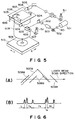
- Figure 5 is a schematic view of a major part of an alignment system as proposed in Japanese Laid-Open Patent Application, Laid-Open No. Sho 53-135653.
- light from a laser 501 passes a lens 601 and is reflected by a rotating polygonal mirror 502.
- the reflected light impinges on an f- ⁇ lens 503 having a characteristic for providing telecentric emission light.
- the f- ⁇ lens 503 has its entrance pupil defined at the reflection surface of the polygonal mirror 502.
- the light passing the f- ⁇ lens 503 enters a lens 602 and impinges on a roof prism 504 by which it is distributed to two, left and right alignment optical systems.
- the left and right alignment optical systems have symmetrical structures and, therefore, only one alignment optical system will be explained below.
- the light distributed by the roof prism 504 is reflected by a half mirror 603 and then goes through a lens 604 and a mirror 605. Then, by an objective lens 505, the light is projected on a reticle 507 surface which is at an image surface of the f- ⁇ lens 503 or at a plane optically conjugate with the image surface, and then on a wafer 509 surface which is at a plane optically conjugate with the reticle 507 surface with respect to a projection lens 508. Rotation of the polygonal mirror 502 is effective to scan the wafer 509 surface in telecentric state.
- reticle alignment marks 507M and wafer alignment marks 509M which may be called "alignment patterns"
- alignment patterns When light passes near the alignment pattern, it is specularly reflected by a part in which no edge of the alignment pattern is present so that what can be called a non-scattered light is produced which goes back along its oncoming path.
- the light At a part in which an edge of the alignment pattern is present, the light is diffracted or irregularly reflected such that what can be called a scattered light is produced which goes back to along its oncoming path.
- the non-scattered light and the scattered light passing through the objective lens 505 goes by way of the mirror 605, the lens 604 and the half mirror603 to a lens 606 and a lens 607. Then, by a slit means (not shown) which is disposed at a position optically conjugate with the pupil plane of the objective lens 505 and which has a central non-transparent area, only the scattered light is allowed to pass therethrough and the light is received by a photodetector (light receiving portion) 511.
- the scattered light from the alignment pattern is detected to detect positional deviation between the reticle 3 and the wafer 1 and, on the basis of this, the position adjustment (alignment) is made.
- Figure 6 part (B) illustrates an output signal from the light receiving portion 511 in an occasion where the positional relationship between the wafer alignment pattern and the mask alignment pattern is such as shown in Figure 6, part (A).
- the axis of abscissa denotes time and the axis of ordinate denotes the level of output.
- the alignment information obtainable with the device shown in Figure 5 is such positional information that is just at a moment when the beam from the laser 501 scanned by the polygonal mirror 502 impinges on the alignment marks of the reticle 507 and the wafer 509.
- GB 2 131 205A discloses a method of discriminating stillness of a step exposure apparatus characterised by the steps of causing a mask and wafer to step relative to each other, repetitively detecting the relative displacement (degree of out-of-alignment) between the mask and wafer, processing to computer a value representing a variation in the displacement measurements, and comparing the computed value with a critical value relating to the attenuation of vibration resulting from the stepping motion to instruct the computation of the amount of further relative movement to be effected between the mask and wafer if the measurement is smaller than the critical value (and assuming the mask and wafer are not yet properly aligned) or to instruct the re-computation of the value if it is larger than the critical value.
- the alignment information obtained in the manner described above contains an error due to the relative vibration of the mask and the wafer.
- Such an error may be disregarded in a conventional alignment process to be made in an exposure apparatus of the type arranged to execute an exposure process of a line-and-space of an order of 1.0 micron.
- an alignment process to be made in an exposure apparatus of the type such as an X-ray stepper, that executes an exposure process of a line-and-space of an order of 0.25 micron, such error can not be disregarded.
- a precision of an order of 0.01 micron is required for the alignment detection.
- the mask-to-wafer alignment information is detected by plural times and, from an average of measured values, the positional error between the mask and the wafer is determined.
- this method requires a procedure of multiple measurements of alignment information as well as detection of an average of measured values. Therefore, it requires a long time for the alignment detection. Further, the measurements are intermittent and there is a possibility that, if the period of intermittent measurement is in a certain relationship with the period of the relative vibration of the mask and the wafer, the result obtained from the multiple measurements still contains an error.
- a light receiving means comprises an accumulation type photoelectric converting element and the accumulation time thereof is suitably set in consideration of the period of a natural vibration frequency (which may be called "resonance frequency") of the relative vibration of the mask and the wafer to be aligned with each other.
- a natural vibration frequency which may be called "resonance frequency”
- the accumulation time of the accumulation type photoelectric converting element may be controlled by using an output signal from a displacement gauge which is provided to detect the natural vibration frequency of the first and second objects.
- the natural vibration frequency of the first and second objects may be measured and the measured value memorized in a part of a memory means of the alignment system, the accumulation time of the accumulation type photoelectric converting element being controlled on the basis of an output signal from the memory means.
- Figure 1 is a schematic and diagrammatic view of a major part of a first embodiment of the present invention.
- a light emitting element which is a semiconductor laser, in this embodiment; and at 102 is a collimator lens for collimating light from the semiconductor laser 101 into a parallel light.
- Denoted at 103 is a half mirror for reflecting the light from the semiconductor laser toward a mask 104 and a wafer 105. Also, it functions to transmit the light coming back from the mask 104 and the wafer 105.
- the mask 104 which is a first object comprises a base film made of polyimide, for example, on which a semiconductor circuit pattern of Au, for example, to be printed on the wafer 105 as well as an alignment mark 104a are formed.
- the alignment mark 104a is provided on one of the surfaces of the mask 104 and is irradiated with the reflected light from the half mirror 103.
- the wafer 105 which is a second object is made of silicon, for example, on which the semiconductor circuit pattern of the mask 104 is to be printed with a suitable exposure energy.
- An alignment mark 105a is formed on the wafer 105.
- Denoted at 106 is an accumulation type photoelectric converting element which is disposed to receive light, having alignment information, coming from the alignment marks 104a and 105a of the mask 104 and the wafer 105, respectively.
- the photoelectric converting element 106 may comprise a CCD line sensor, for example.
- LD driver 107 serves to actuate the semiconductor laser 101 at an externally set light quantity.
- Sensor driver 108 serves to controllably drive the photoelectric converting element 106 with an externally set accumulation time.
- Signal processing unit 109 serves to process the output of the photoelectric converting element 106 and to calculate, as an example, the center of gravity of light which bears the positional information.
- Displacement gauge 110 is provided to measure the relative vibration of the mask 104 and the wafer 105, and it comprises an electrostatic capacitance type displacement gauge, for example.
- Microcomputer 110 receives an output of the displacement gauge 110 and operates, on the basis of the relative vibration of the mask 104 and the wafer 105, to set the quantity of light to be provided by the semiconductor laser 101 and also to set the accumulation time of the photoelectric converting element 106, the microcomputer producing and supplying corresponding signal to the LD driver 107 and the sensor driver 108.
- the mark 104a of the mask 104 (hereinafter, the mark 104a will be referred to simply as "mask”) and the alignment mark 105a of the wafer 105 (hereinafter, the mark 105a will be referred to simply as "wafer”)
- the alignment information required in a semiconductor device manufacturing exposure apparatus is the average position S of the mask and the wafer.
- the signal processing unit 109 processes the output S'(i) of the photoelectric converting element (hereinafter "line sensor") 106, and calculates the relative position of the mask and the wafer.
- S'(i) denotes the output of the i-th one of plural detecting elements (of a number m) that constitute the line sensor 106.
- the i-th output S'(i) of the line sensor 106 is one that has been obtained as a result of impingement on the line sensor 106 of the light bearing the information on the sum of the relative position S of the mask and the wafer and the deviation N(t) due to the relative vibration of the mask and the wafer. If these light components are denoted by LS(i) and LN(i,t), then, the output S'(i) from the line sensor 106 corresponds to the result of integration, with the accumulation time Ct, of the aforementioned light incident on the line sensor 106. Thus, it can be expressed as follows: wherein K is the detection sensitivity of the line sensor 106.
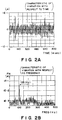
- the relative vibration of the mask 104 and the wafer 105 is minute vibration such as illustrated in Figure 2A.
- the relative vibration of the mask 104 and the wafer 105 is such a system as having a natural vibration frequency at 105 (Hz).
- Twm 1/fwm Since, as for the amplitude of the relative vibration of the mask 104 and the wafer 105, one deriving from the natural vibration frequency fwm is dominant, if the accumulation time Ct is made sufficiently longer than the period Twm, namely, Ct >> Twm and thus, then, the effect of the deviation N(t) on the output S'(i) is reduced.
- the output S'(i) as expressed by equation (1) may be considered as: If the accumulation time Ct is made four or five times longer than the period Twm, then, the signal to-noise ratio of the output S'(i), that is, can be increased by one figure or more. Therefore, taking the output S'(i) as being represented by equation (2) does not cause inconveniences.
- n is an integral number not less than 4.
- the accumulation time is four or five times larger than the period Twm.
- the position S' of the mask and the wafer detected by the signal processing unit 109 contains an error E which results from an optical error or a processing error.
- the accumulation time of the line sensor 106 is selected and set so as to be sufficiently longer than the period Twm of the natural vibration frequency fwm of the relative vibration of the mask and the wafer, more particularly, it is selected and set to the n times larger than the period Twm, wherein n is an integral number not less than 4. If this is done, the output S'(i) of the line sensor 106 is hardly influenced by the relative vibration of the mask and the wafer and, therefore, with regard to the position S' of the mask and the wafer detected by the signal processing unit 109 on the basis of the output of the line sensor 106 it is sufficient to take into account only the error E resulting from the optical error or processing error.
- equation (10) it follows that: S' ⁇ S(t) + E
- the accumulation time Ct of the line sensor 106 is set to be longer than the period Twm of the natural vibration frequency fwm of the relative vibration of the mask 104 and the wafer 105. More particularly, the accumulation time Ct of the line sensor 106 is set to be equal to a multiple, by an integral number, of the period Twm of the natural vibration frequency fwm of the relative vibration of the mask 104 and the wafer 105.
- the accumulation time Ct of the line sensor 106 is set to be equal to a multiple, by an integral number, of the period Twm of the natural vibration frequency fwm of the relative vibration of the mask 104 and the wafer 105.
- the sensitivity of the line sensor 106 changes with the accumulation time Ct in a manner such as, for example, illustrated in Figure 3.
- the accumulation time Ct of the line sensor 106 is modified to be equal to a multiple, by an integral number, of the period Twm of the natural vibration frequency fwm of the relative vibration of the mask 104 and the wafer 105, the sensitivity of the line sensor 106 changes.
- the output of the line sensor 106 is to be processed by the signal processing unit 109, it is desirable that the output is high within a non-saturation range. It is therefore necessary to control the output of the line sensor 106 to an optimum value as required by the signal processing unit 109.
- Figure 4 is a schematic and diagrammatic view of a major part of a second embodiment of the present invention.
- like numerals as used in Figure 1 are assigned to the elements corresponding to those in the Figure 1 example.
- a microcomputer 111 cooperates with an electrostatic capacitance type displacement gauge (not shown) or otherwise to measure, in preparation, the period Twm of the natural vibration frequency fwm of the relative vibration of the mask 104 and the wafer 105.
- the measured value is memorized in a memory means within the microcomputer 111 or in a memory means provided in the exposure apparatus.
- the measured value (data) is transmitted as required to an LD driver 107 or a sensor driver 108.
- the period Twm of the natural vibration frequency fwm of the relative vibration of the mask 104 and the wafer 105 hardly changes. Accordingly, only by preparatory measurement of the period Twm of the natural vibration frequency fwm of the relative vibration of the mask 104 and the wafer 105, which is dependent upon the apparatus, that is, only by setting through the microcomputer 111 the accumulation time which is determined in accordance with the period Twm, substantially the same advantageous effects as described hereinbefore are attainable in the present embodiment.
- the system in place of using the microcomputer 111 shown in Figure 4, the system may be structured with a hardware in which a certain fixed accumulation time is determined on the basis of the period Twm of the natural vibration frequency fwm of the relative vibration of the mask 104 and the wafer 105 as measured in preparation by using an electrostatic capacitance type displacement gauge (not shown) or otherwise. Substantially the same effects are attainable.
- the photoelectric converting element comprises a line sensor such as CCD or the like.
- the accumulation time is controllable, any type of photoelectric converting element may be used.
- a CCD area sensor may be used.
- an accumulation type photoelectric converting element is used as a light receiving means and the accumulation time is selected and set in accordance with the period of the natural vibration frequency of relative vibration of a mask and a wafer to be aligned with each other.
- the former is selected to be longer than the latter, more particularly, to be equal to a multiple, by an integral number, of the latter.
- the present invention can provide an alignment system having advantageous features that, as compared with the conventional method which requires a procedure of multiple measurements of the alignment information and subsequent averaging of measured values to obtain average alignment information, the time for the alignment detection can be shortened and, therefore, the throughput of the exposure apparatus as a whole can be increased.
Landscapes
- Physics & Mathematics (AREA)
- General Physics & Mathematics (AREA)
- Exposure And Positioning Against Photoresist Photosensitive Materials (AREA)
- Exposure Of Semiconductors, Excluding Electron Or Ion Beam Exposure (AREA)
- Length Measuring Devices By Optical Means (AREA)
Description
- This invention relates generally to an alignment system and method for correctly positioning an object. More particularly, the invention is concerned with position detecting method and apparatus suitably usable, for example, in a semiconductor microcircuit device manufacturing exposure apparatus for lithographically transferring a fine electronic circuit pattern formed on the surface of a first object (original) such as a mask or reticle (hereinafter simply "mask") onto the surface of a second object (workpiece) such as a wafer, for relatively positioning or aligning the mask and the wafer.
- In exposure apparatuses for use in the manufacture of semiconductor devices, the relative alignment of a mask and a wafer is one important factor in respect to ensuring improved performance. Particularly, as for alignment system employed in recent exposure apparatuses, submicron alignment accuracies or more strict accuracies are required in consideration of the demand for higher degree of integration of semiconductor devices.
- In many types of alignment systems, features called "alignment patterns" are provided on a mask and a wafer and, by utilizing positional information obtainable from these patterns, the mask and wafer are aligned.
- Figure 5 is a schematic view of a major part of an alignment system as proposed in Japanese Laid-Open Patent Application, Laid-Open No. Sho 53-135653.
- In Figure 5, light from a
laser 501 passes alens 601 and is reflected by a rotatingpolygonal mirror 502. The reflected light impinges on an f-θ lens 503 having a characteristic for providing telecentric emission light. The f-θ lens 503 has its entrance pupil defined at the reflection surface of thepolygonal mirror 502. The light passing the f-θ lens 503 enters alens 602 and impinges on aroof prism 504 by which it is distributed to two, left and right alignment optical systems. - In the Figure 5 example, the left and right alignment optical systems have symmetrical structures and, therefore, only one alignment optical system will be explained below.
- The light distributed by the
roof prism 504 is reflected by ahalf mirror 603 and then goes through alens 604 and amirror 605. Then, by anobjective lens 505, the light is projected on areticle 507 surface which is at an image surface of the f-θ lens 503 or at a plane optically conjugate with the image surface, and then on awafer 509 surface which is at a plane optically conjugate with thereticle 507 surface with respect to aprojection lens 508. Rotation of thepolygonal mirror 502 is effective to scan thewafer 509 surface in telecentric state. - On the
reticle 507 surface and thewafer 509 surface, there are provided identification marks for alignment purpose such as illustrated in Figure 6, part (A). More specifically, there are formedreticle alignment marks 507M andwafer alignment marks 509M (which may be called "alignment patterns"), at two left and right sites. When light passes near the alignment pattern, it is specularly reflected by a part in which no edge of the alignment pattern is present so that what can be called a non-scattered light is produced which goes back along its oncoming path. At a part in which an edge of the alignment pattern is present, the light is diffracted or irregularly reflected such that what can be called a scattered light is produced which goes back to along its oncoming path. - Of these rays, the non-scattered light and the scattered light passing through the
objective lens 505 goes by way of themirror 605, thelens 604 and the half mirror603 to alens 606 and alens 607. Then, by a slit means (not shown) which is disposed at a position optically conjugate with the pupil plane of theobjective lens 505 and which has a central non-transparent area, only the scattered light is allowed to pass therethrough and the light is received by a photodetector (light receiving portion) 511. - In the Figure 5 example, the scattered light from the alignment pattern is detected to detect positional deviation between the
reticle 3 and thewafer 1 and, on the basis of this, the position adjustment (alignment) is made. - Figure 6, part (B), illustrates an output signal from the
light receiving portion 511 in an occasion where the positional relationship between the wafer alignment pattern and the mask alignment pattern is such as shown in Figure 6, part (A). The axis of abscissa denotes time and the axis of ordinate denotes the level of output. - Positional errors between the alignment marks of the
reticle 507 and thewafer 509 can be determined, by using the characters referred to in Figure 6(B), in the following manner:

- The alignment information obtainable with the device shown in Figure 5 is such positional information that is just at a moment when the beam from the
laser 501 scanned by thepolygonal mirror 502 impinges on the alignment marks of thereticle 507 and thewafer 509. -
GB 2 131 205A discloses a method of discriminating stillness of a step exposure apparatus characterised by the steps of causing a mask and wafer to step relative to each other, repetitively detecting the relative displacement (degree of out-of-alignment) between the mask and wafer, processing to computer a value representing a variation in the displacement measurements, and comparing the computed value with a critical value relating to the attenuation of vibration resulting from the stepping motion to instruct the computation of the amount of further relative movement to be effected between the mask and wafer if the measurement is smaller than the critical value (and assuming the mask and wafer are not yet properly aligned) or to instruct the re-computation of the value if it is larger than the critical value. - In a semiconductor device manufacturing exposure apparatus, due to various factors, a mask and a semiconductor wafer are vibrating. For this reason, the alignment information obtained in the manner described above contains an error due to the relative vibration of the mask and the wafer. Such an error may be disregarded in a conventional alignment process to be made in an exposure apparatus of the type arranged to execute an exposure process of a line-and-space of an order of 1.0 micron. However, in an alignment process to be made in an exposure apparatus of the type, such as an X-ray stepper, that executes an exposure process of a line-and-space of an order of 0.25 micron, such error can not be disregarded. In this type of exposure apparatuses, a precision of an order of 0.01 micron is required for the alignment detection.
- By way of example, in an attempt to solving this problem, one may consider such a method that the mask-to-wafer alignment information is detected by plural times and, from an average of measured values, the positional error between the mask and the wafer is determined.
- However, this method requires a procedure of multiple measurements of alignment information as well as detection of an average of measured values. Therefore, it requires a long time for the alignment detection. Further, the measurements are intermittent and there is a possibility that, if the period of intermittent measurement is in a certain relationship with the period of the relative vibration of the mask and the wafer, the result obtained from the multiple measurements still contains an error.
- It is accordingly an object of the present invention to provide an improved alignment system by which a mask and a wafer can be aligned with high precision.
- In an aspect of the present invention, a light receiving means comprises an accumulation type photoelectric converting element and the accumulation time thereof is suitably set in consideration of the period of a natural vibration frequency (which may be called "resonance frequency") of the relative vibration of the mask and the wafer to be aligned with each other.
- According to the invention there is provided an alignment system having features as recited in
claim 1. - The accumulation time of the accumulation type photoelectric converting element may be controlled by using an output signal from a displacement gauge which is provided to detect the natural vibration frequency of the first and second objects.
- The natural vibration frequency of the first and second objects may be measured and the measured value memorized in a part of a memory means of the alignment system, the accumulation time of the accumulation type photoelectric converting element being controlled on the basis of an output signal from the memory means.
- Advantages of the present invention will become more apparent upon a consideration of the following description of the preferred embodiments of the present invention taken in conjunction with the accompanying drawings in which:-
- Figure 1 is a schematic and diagrammatic view of a major part of an alignment system according to a first embodiment of the present invention.
- Figures 2A and 2B illustrate the results of measurement of deviation due to the relative vibration of a mask and a wafer.
- Figure 3 illustrates the photoelectric conversion property of an accumulation type sensor.
- Figure 4 is a schematic and diagrammatic view of a major part of an alignment system according to a second embodiment of the present invention.
- Figure 5 is a perspective view schematically showing a known type alignment system.
- Figure 6 illustrates an output of a photodetector of the Figure 5 example.
- Figure 1 is a schematic and diagrammatic view of a major part of a first embodiment of the present invention. In Figure 1, denoted at 101 is a light emitting element which is a semiconductor laser, in this embodiment; and at 102 is a collimator lens for collimating light from the
semiconductor laser 101 into a parallel light. Denoted at 103 is a half mirror for reflecting the light from the semiconductor laser toward amask 104 and awafer 105. Also, it functions to transmit the light coming back from themask 104 and thewafer 105. Themask 104 which is a first object comprises a base film made of polyimide, for example, on which a semiconductor circuit pattern of Au, for example, to be printed on thewafer 105 as well as analignment mark 104a are formed. Thealignment mark 104a is provided on one of the surfaces of themask 104 and is irradiated with the reflected light from thehalf mirror 103. Thewafer 105 which is a second object is made of silicon, for example, on which the semiconductor circuit pattern of themask 104 is to be printed with a suitable exposure energy. Analignment mark 105a is formed on thewafer 105. Denoted at 106 is an accumulation type photoelectric converting element which is disposed to receive light, having alignment information, coming from thealignment marks mask 104 and thewafer 105, respectively. Thephotoelectric converting element 106 may comprise a CCD line sensor, for example. -
LD driver 107 serves to actuate thesemiconductor laser 101 at an externally set light quantity.Sensor driver 108 serves to controllably drive thephotoelectric converting element 106 with an externally set accumulation time.Signal processing unit 109 serves to process the output of thephotoelectric converting element 106 and to calculate, as an example, the center of gravity of light which bears the positional information.Displacement gauge 110 is provided to measure the relative vibration of themask 104 and thewafer 105, and it comprises an electrostatic capacitance type displacement gauge, for example. -
Microcomputer 110 receives an output of thedisplacement gauge 110 and operates, on the basis of the relative vibration of themask 104 and thewafer 105, to set the quantity of light to be provided by thesemiconductor laser 101 and also to set the accumulation time of thephotoelectric converting element 106, the microcomputer producing and supplying corresponding signal to theLD driver 107 and thesensor driver 108. - In the present embodiment, where the average position of the
alignment mark 104a of the mask 104 (hereinafter, themark 104a will be referred to simply as "mask") and thealignment mark 105a of the wafer 105 (hereinafter, themark 105a will be referred to simply as "wafer"), is denoted by S, such position as combined with a deviation N(t) which is variable with time due to the relative vibration of the mask and the wafer, is the actual relative position S(t) of the mask and the wafer at a moment t. Namely, a relationship:
- Generally, the alignment information required in a semiconductor device manufacturing exposure apparatus is the average position S of the mask and the wafer. Conventionally, the deviation N(t) due to the relative vibration of the mask and the wafer is quite small as compared with the required resolution for the mask-to-wafer position S. Therefore, it follows that:

- The
signal processing unit 109 processes the output S'(i) of the photoelectric converting element (hereinafter "line sensor") 106, and calculates the relative position of the mask and the wafer. Here, S'(i) denotes the output of the i-th one of plural detecting elements (of a number m) that constitute theline sensor 106. - The i-th output S'(i) of the
line sensor 106 is one that has been obtained as a result of impingement on theline sensor 106 of the light bearing the information on the sum of the relative position S of the mask and the wafer and the deviation N(t) due to the relative vibration of the mask and the wafer. If these light components are denoted by LS(i) and LN(i,t), then, the output S'(i) from theline sensor 106 corresponds to the result of integration, with the accumulation time Ct, of the aforementioned light incident on theline sensor 106. Thus, it can be expressed as follows:
line sensor 106. - As for the deviation N(t) due to the relative vibration of the mask and the wafer, chiefly, one resulting from the mechanical resonance of structural parts supporting the
mask 104 and thewafer 105 is dominant. For example, in the present embodiment, it has been confirmed by actual measurement that the relative vibration of themask 104 and thewafer 105 is minute vibration such as illustrated in Figure 2A. Further, as a result of measurement, it has been confirmed that, such as shown in Figure 2B, the relative vibration of themask 104 and thewafer 105 is such a system as having a natural vibration frequency at 105 (Hz). - The period Twm of the natural vibration frequency to the natural vibration frequency fwm of the relative vibration of the
mask 104 and thewafer 105 is:
mask 104 and thewafer 105, one deriving from the natural vibration frequency fwm is dominant, if the accumulation time Ct is made sufficiently longer than the period Twm, namely,


- Setting an accumulation time Ct which is n times larger than the period Twm (where n is an integral number), rather than setting the time Ct to be sufficient longer than the period Twm or in addition to doing so, is also effective to reduce the effect of the deviation (t) upon the output S'(i). That is, if


- If the number of the detecting elements (i.e., the number of bits) of the
line sensor 106 is denoted by m and the signal processing by thesignal processing unit 109 is represented by F, then the position S' of themask 104 and thewater 105 to be detected by thesignal processing unit 109, can be expressed as follows:
wherein i = 1 - m - Generally, the position S' of the mask and the wafer detected by the
signal processing unit 109 contains an error E which results from an optical error or a processing error. Namely,
That is:
- In the present embodiment, the accumulation time of the
line sensor 106 is selected and set so as to be sufficiently longer than the period Twm of the natural vibration frequency fwm of the relative vibration of the mask and the wafer, more particularly, it is selected and set to the n times larger than the period Twm, wherein n is an integral number not less than 4. If this is done, the output S'(i) of theline sensor 106 is hardly influenced by the relative vibration of the mask and the wafer and, therefore, with regard to the position S' of the mask and the wafer detected by thesignal processing unit 109 on the basis of the output of theline sensor 106 it is sufficient to take into account only the error E resulting from the optical error or processing error. Thus, from equation (10), it follows that:
- As described in the foregoing, in Figure 1 the accumulation time Ct of the
line sensor 106 is set to be longer than the period Twm of the natural vibration frequency fwm of the relative vibration of themask 104 and thewafer 105. More particularly, the accumulation time Ct of theline sensor 106 is set to be equal to a multiple, by an integral number, of the period Twm of the natural vibration frequency fwm of the relative vibration of themask 104 and thewafer 105. Thus, in regard to the position S' of the mask and the wafer as detected by thesignal processing unit 109, it is sufficient to taken into account only the error E which result from an optical error or processing error. Therefore, the following equation is obtained:
- On the other hand, the sensitivity of the
line sensor 106 changes with the accumulation time Ct in a manner such as, for example, illustrated in Figure 3. - As an example, if the accumulation time Ct of the
line sensor 106 is modified to be equal to a multiple, by an integral number, of the period Twm of the natural vibration frequency fwm of the relative vibration of themask 104 and thewafer 105, the sensitivity of theline sensor 106 changes. - When the output of the
line sensor 106 is to be processed by thesignal processing unit 109, it is desirable that the output is high within a non-saturation range. It is therefore necessary to control the output of theline sensor 106 to an optimum value as required by thesignal processing unit 109. - To this end, in the present embodiment, for providing an optimum output of the
line sensor 106, the accumulation time Ct of theline sensor 106 is adjusted so that the optical output Pℓd of thesemiconductor laser 106 satisfies the following condition:
displacement gauge 110 and then sets an optimum accumulation time Ct of theline sensor 106. Then, an optimum value of the optical output Pℓd of thesemiconductor laser 101, to the accumulation time Ct of theline sensor 106, is set. - Figure 4 is a schematic and diagrammatic view of a major part of a second embodiment of the present invention. In Figure 4, like numerals as used in Figure 1 are assigned to the elements corresponding to those in the Figure 1 example.
- In Figure 4, a microcomputer 111 cooperates with an electrostatic capacitance type displacement gauge (not shown) or otherwise to measure, in preparation, the period Twm of the natural vibration frequency fwm of the relative vibration of the
mask 104 and thewafer 105. The measured value is memorized in a memory means within the microcomputer 111 or in a memory means provided in the exposure apparatus. The measured value (data) is transmitted as required to anLD driver 107 or asensor driver 108. - In an apparatus such as a semiconductor device manufacturing exposure apparatus, even if a mask or a wafer changes, mechanical resonance of a massive stage or other structural parts is dominant. Therefore, the period Twm of the natural vibration frequency fwm of the relative vibration of the
mask 104 and thewafer 105 hardly changes. Accordingly, only by preparatory measurement of the period Twm of the natural vibration frequency fwm of the relative vibration of themask 104 and thewafer 105, which is dependent upon the apparatus, that is, only by setting through the microcomputer 111 the accumulation time which is determined in accordance with the period Twm, substantially the same advantageous effects as described hereinbefore are attainable in the present embodiment. - Further, in the present embodiment, in place of using the microcomputer 111 shown in Figure 4, the system may be structured with a hardware in which a certain fixed accumulation time is determined on the basis of the period Twm of the natural vibration frequency fwm of the relative vibration of the
mask 104 and thewafer 105 as measured in preparation by using an electrostatic capacitance type displacement gauge (not shown) or otherwise. Substantially the same effects are attainable. - In each of the foregoing embodiments, the photoelectric converting element comprises a line sensor such as CCD or the like. However, provided that the accumulation time is controllable, any type of photoelectric converting element may be used. For example, a CCD area sensor may be used.
- In accordance with the present invention, as described hereinbefore, an accumulation type photoelectric converting element is used as a light receiving means and the accumulation time is selected and set in accordance with the period of the natural vibration frequency of relative vibration of a mask and a wafer to be aligned with each other. For example, the former is selected to be longer than the latter, more particularly, to be equal to a multiple, by an integral number, of the latter. By this, it becomes possible to obtain an average of alignment information that contains deviation resulting from the relative vibration of the mask and the wafer.
- Thus, the present invention can provide an alignment system having advantageous features that, as compared with the conventional method which requires a procedure of multiple measurements of the alignment information and subsequent averaging of measured values to obtain average alignment information, the time for the alignment detection can be shortened and, therefore, the throughput of the exposure apparatus as a whole can be increased.
Claims (8)
- An alignment system for aligning first and second objects by using alignment marks, said system comprising: a light source (101); an accumulation type photoelectric converting device (106); and an optical arrangement (102, 103) for directing light from said light source to the alignment marks and then to said photoelectric converting device;characterised by control means (111) adapted for storing the period of natural vibration frequency with respect to relative vibration of the first and second objects, and for determining and controlling the accumulation time of said photoelectric converting device, on the basis of the stored period, so that the controlled accumulation time of said photoelectric converting device is longer than said stored period.
- A system as claimed in claim 1, characterised in that the controlled accumulation time of said photoelectric converting device is substantially equal to a positive integer multiple of said stored period.
- A system as claimed in claim 1, characterised in that the controlled accumulation time of said photoelectric converting device is substantially equal to a multiple, by an integer not less than four, of said stored period.
- A system as claimed in claim 1, 2 or 3, characterised in that detecting means (110) are provided for detecting a natural vibration period of the first and second objects.
- An alignment method for aligning first and second objects having alignment marks respectively, using a system comprising a light source (101); an accumulation type photoelectric converting device; and an optical arrangement (102, 103) for directing light from said light source to the alignment marks and then to said photoelectric converting device; comprising storing the period of natural vibration frequency with respect to relative vibration of the first and second objects in control means (111), and determining and controlling the accumulation time of said photoelectric converting device, on the basis of the stored period, by said control means so that the controlled accumulation time of said photoelectric converting device is longer than said stored period.
- A method as claimed in claim 5, characterised in that the controlled accumulation time of said photoelectric converting device is substantially equal to a positive integer multiple of said stored period.
- A method as claimed in claim 5, characterised in that the controlled accumulation time of said photoelectric converting device is substantially equal to a multiple, by an integer not less than four, of said stored period.
- A method as claimed in claims 5, 6 or 7, characterised in that said accumulation time of said photoelectric converting device is equal to a multiple, by a positive integer, of the natural vibration frequency of the first and second objects.
Applications Claiming Priority (2)
| Application Number | Priority Date | Filing Date | Title |
|---|---|---|---|
| JP63246648A JP2734004B2 (en) | 1988-09-30 | 1988-09-30 | Positioning device |
| JP246648/88 | 1988-09-30 |
Publications (3)
| Publication Number | Publication Date |
|---|---|
| EP0361933A2 EP0361933A2 (en) | 1990-04-04 |
| EP0361933A3 EP0361933A3 (en) | 1991-04-03 |
| EP0361933B1 true EP0361933B1 (en) | 1996-02-14 |
Family
ID=17151540
Family Applications (1)
| Application Number | Title | Priority Date | Filing Date |
|---|---|---|---|
| EP89309914A Expired - Lifetime EP0361933B1 (en) | 1988-09-30 | 1989-09-28 | Alignment system |
Country Status (4)
| Country | Link |
|---|---|
| US (1) | US5028797A (en) |
| EP (1) | EP0361933B1 (en) |
| JP (1) | JP2734004B2 (en) |
| DE (1) | DE68925665T2 (en) |
Families Citing this family (26)
| Publication number | Priority date | Publication date | Assignee | Title |
|---|---|---|---|---|
| JP2704001B2 (en) * | 1989-07-18 | 1998-01-26 | キヤノン株式会社 | Position detection device |
| JP2756331B2 (en) * | 1990-01-23 | 1998-05-25 | キヤノン株式会社 | Interval measuring device |
| EP0634702B1 (en) * | 1990-03-27 | 2010-01-20 | Canon Kabushiki Kaisha | Measuring method and apparatus |
| US5200800A (en) * | 1990-05-01 | 1993-04-06 | Canon Kabushiki Kaisha | Position detecting method and apparatus |
| US5250797A (en) * | 1990-10-05 | 1993-10-05 | Canon Kabushiki Kaisha | Exposure method and apparatus for controlling light pulse emission using determined exposure quantities and control parameters |
| US5418613A (en) * | 1990-11-20 | 1995-05-23 | Canon Kabushiki Kaisha | Method and apparatus for detecting the position of a substrate having first and second patterns of different sizes |
| US5241188A (en) * | 1991-02-01 | 1993-08-31 | Nikon Corporation | Apparatus for detecting a focussing position |
| JPH05152186A (en) * | 1991-05-01 | 1993-06-18 | Canon Inc | Measuring apparatus and exposure apparatus and positioning method for exposure apparatus |
| JPH0540013A (en) * | 1991-08-05 | 1993-02-19 | Canon Inc | Deviation measuring method and exposing device using it |
| US5276337A (en) * | 1991-10-31 | 1994-01-04 | International Business Machines Corporation | Accuracy of alignment and O/L measurement systems by means of tunable source and handling of signal |
| US5495336A (en) * | 1992-02-04 | 1996-02-27 | Canon Kabushiki Kaisha | Position detecting method for detecting a positional relationship between a first object and a second object |
| JP3008654B2 (en) * | 1992-02-21 | 2000-02-14 | キヤノン株式会社 | Position detection device |
| US5303034A (en) * | 1992-05-01 | 1994-04-12 | Storage Technology Corporation | Robotics targeting system |
| US5861952A (en) * | 1992-11-16 | 1999-01-19 | Canon Kabushiki Kaisha | Optical inspection method and apparatus including intensity modulation of a light beam and detection of light scattered at an inspection position |
| US5432603A (en) * | 1992-11-20 | 1995-07-11 | Canon Kabushiki Kaisha | Optical heterodyne interference measuring apparatus and method, and exposing apparatus and device manufacturing method using the same, in which a phase difference between beat signals is detected |
| JPH0786121A (en) * | 1993-06-30 | 1995-03-31 | Canon Inc | Shift measuring method and position detector employing the same |
| JPH0743313A (en) * | 1993-07-29 | 1995-02-14 | Canon Inc | Foreign matter inspection system and production of semiconductor device using it |
| US6005255A (en) * | 1994-05-18 | 1999-12-21 | Symbol Technologies, Inc. | Timing synchronization for image scanning |
| US5959286A (en) * | 1994-05-18 | 1999-09-28 | Symbol Technologies, Inc. | Method and apparatus for raster scanning of images |
| WO2005057174A2 (en) * | 2003-12-08 | 2005-06-23 | Rosenthal Robert D | Method and apparatus for low blood glucose level detection |
| US7854524B2 (en) * | 2007-09-28 | 2010-12-21 | Anorad Corporation | High stiffness low mass supporting structure for a mirror assembly |
| EP2131243B1 (en) * | 2008-06-02 | 2015-07-01 | ASML Netherlands B.V. | Lithographic apparatus and method for calibrating a stage position |
| US7951615B2 (en) * | 2009-04-01 | 2011-05-31 | Taiwan Semiconductor Manufacturing Company, Ltd. | System and method for implementing multi-resolution advanced process control |
| TWI499876B (en) * | 2009-12-09 | 2015-09-11 | Pc Fan Technology Inc | Method for monitoring semiconductor device |
| NL2007634A (en) * | 2010-12-13 | 2012-06-15 | Asml Netherlands Bv | Lithographic apparatus and method. |
| JP6584170B2 (en) * | 2015-07-02 | 2019-10-02 | キヤノン株式会社 | Detection apparatus, lithographic apparatus, article manufacturing method, and detection method |
Family Cites Families (13)
| Publication number | Priority date | Publication date | Assignee | Title |
|---|---|---|---|---|
| JPS53135653A (en) * | 1977-05-01 | 1978-11-27 | Canon Inc | Photoelectric detecting optical device |
| JPS55101804A (en) * | 1979-01-31 | 1980-08-04 | Toshiba Corp | Positioning apparatus |
| US4398824A (en) * | 1981-04-15 | 1983-08-16 | Bell Telephone Laboratories, Incorporated | Wafer tilt compensation in zone plate alignment system |
| JPS57204405A (en) * | 1981-06-12 | 1982-12-15 | Hitachi Ltd | Plate thickness measuring device |
| JPS5994419A (en) * | 1982-11-19 | 1984-05-31 | Canon Inc | Alignment method in divided baking device |
| US4634876A (en) * | 1983-05-13 | 1987-01-06 | Canon Kabushiki Kaisha | Object position detecting apparatus using accumulation type sensor |
| US4725737A (en) * | 1984-11-13 | 1988-02-16 | Hitachi, Ltd. | Alignment method and apparatus for reduction projection type aligner |
| US4714331A (en) * | 1985-03-25 | 1987-12-22 | Canon Kabushiki Kaisha | Method and apparatus for automatic focusing |
| JP2526546B2 (en) * | 1986-04-21 | 1996-08-21 | 日本電気株式会社 | Alignment device |
| DE3719538A1 (en) * | 1986-06-11 | 1987-12-17 | Toshiba Kawasaki Kk | METHOD AND DEVICE FOR ADJUSTING A SPLIT BETWEEN TWO OBJECTS TO A PREDICTED SIZE |
| US4728193A (en) * | 1986-12-11 | 1988-03-01 | Hughes Aircraft Company | Precision automatic mask-wafer alignment system |
| US4815854A (en) * | 1987-01-19 | 1989-03-28 | Nec Corporation | Method of alignment between mask and semiconductor wafer |
| JP2569544B2 (en) * | 1987-04-08 | 1997-01-08 | 株式会社ニコン | Positioning device |
-
1988
- 1988-09-30 JP JP63246648A patent/JP2734004B2/en not_active Expired - Fee Related
-
1989
- 1989-09-28 US US07/413,739 patent/US5028797A/en not_active Expired - Lifetime
- 1989-09-28 DE DE68925665T patent/DE68925665T2/en not_active Expired - Fee Related
- 1989-09-28 EP EP89309914A patent/EP0361933B1/en not_active Expired - Lifetime
Also Published As
| Publication number | Publication date |
|---|---|
| DE68925665T2 (en) | 1996-07-11 |
| EP0361933A2 (en) | 1990-04-04 |
| JP2734004B2 (en) | 1998-03-30 |
| US5028797A (en) | 1991-07-02 |
| DE68925665D1 (en) | 1996-03-28 |
| EP0361933A3 (en) | 1991-04-03 |
| JPH0293305A (en) | 1990-04-04 |
Similar Documents
| Publication | Publication Date | Title |
|---|---|---|
| EP0361933B1 (en) | Alignment system | |
| US4801977A (en) | Projection optical apparatus | |
| US6081614A (en) | Surface position detecting method and scanning exposure method using the same | |
| US5602400A (en) | Surface position detecting method and apparatus including detection and correction of errors, such as surface position errors or tilt, in exposure regions | |
| US5742067A (en) | Exposure method and apparatus therefor | |
| US6057908A (en) | Exposure condition measurement method | |
| US5920398A (en) | Surface position detecting method and scanning exposure method using the same | |
| US6534777B2 (en) | Surface position detecting system and method having a sensor selection | |
| US4705940A (en) | Focus detection in a projection optical system | |
| US5729337A (en) | Inclination detecting apparatus | |
| US4566795A (en) | Alignment apparatus | |
| US7668343B2 (en) | Surface position measuring method and apparatus | |
| US5596204A (en) | Method for aligning processing areas on a substrate with a predetermined position in a static coordinate system | |
| US5396335A (en) | Position detecting method | |
| US5936711A (en) | Projection exposure method and projection exposure apparatus | |
| JPH1064814A (en) | Surface position detecting device and manufacture of device using it | |
| US7072027B2 (en) | Exposure apparatus, method of controlling same, and method of manufacturing devices | |
| US6473156B2 (en) | Scanning exposure apparatus and device manufacturing method | |
| JP3203676B2 (en) | Projection exposure equipment | |
| JPH10209030A (en) | Method and apparatus for projection exposure | |
| JP2001185474A (en) | Alignment method, alignment device, substrate, mask, and exposure device | |
| EP0474487B1 (en) | Method and device for optically detecting position of an article |
Legal Events
| Date | Code | Title | Description |
|---|---|---|---|
| PUAI | Public reference made under article 153(3) epc to a published international application that has entered the european phase |
Free format text: ORIGINAL CODE: 0009012 |
|
| AK | Designated contracting states |
Kind code of ref document: A2 Designated state(s): DE FR GB NL |
|
| PUAL | Search report despatched |
Free format text: ORIGINAL CODE: 0009013 |
|
| 17P | Request for examination filed |
Effective date: 19901231 |
|
| AK | Designated contracting states |
Kind code of ref document: A3 Designated state(s): DE FR GB NL |
|
| 17Q | First examination report despatched |
Effective date: 19931116 |
|
| GRAA | (expected) grant |
Free format text: ORIGINAL CODE: 0009210 |
|
| AK | Designated contracting states |
Kind code of ref document: B1 Designated state(s): DE FR GB NL |
|
| REF | Corresponds to: |
Ref document number: 68925665 Country of ref document: DE Date of ref document: 19960328 |
|
| ET | Fr: translation filed | ||
| PLBE | No opposition filed within time limit |
Free format text: ORIGINAL CODE: 0009261 |
|
| STAA | Information on the status of an ep patent application or granted ep patent |
Free format text: STATUS: NO OPPOSITION FILED WITHIN TIME LIMIT |
|
| 26N | No opposition filed | ||
| REG | Reference to a national code |
Ref country code: GB Ref legal event code: IF02 |
|
| PGFP | Annual fee paid to national office [announced via postgrant information from national office to epo] |
Ref country code: GB Payment date: 20040915 Year of fee payment: 16 |
|
| PGFP | Annual fee paid to national office [announced via postgrant information from national office to epo] |
Ref country code: NL Payment date: 20040923 Year of fee payment: 16 |
|
| PGFP | Annual fee paid to national office [announced via postgrant information from national office to epo] |
Ref country code: FR Payment date: 20040927 Year of fee payment: 16 |
|
| PGFP | Annual fee paid to national office [announced via postgrant information from national office to epo] |
Ref country code: DE Payment date: 20041124 Year of fee payment: 16 |
|
| PG25 | Lapsed in a contracting state [announced via postgrant information from national office to epo] |
Ref country code: GB Free format text: LAPSE BECAUSE OF NON-PAYMENT OF DUE FEES Effective date: 20050928 |
|
| PG25 | Lapsed in a contracting state [announced via postgrant information from national office to epo] |
Ref country code: NL Free format text: LAPSE BECAUSE OF NON-PAYMENT OF DUE FEES Effective date: 20060401 Ref country code: DE Free format text: LAPSE BECAUSE OF NON-PAYMENT OF DUE FEES Effective date: 20060401 |
|
| GBPC | Gb: european patent ceased through non-payment of renewal fee |
Effective date: 20050928 |
|
| PG25 | Lapsed in a contracting state [announced via postgrant information from national office to epo] |
Ref country code: FR Free format text: LAPSE BECAUSE OF NON-PAYMENT OF DUE FEES Effective date: 20060531 |
|
| NLV4 | Nl: lapsed or anulled due to non-payment of the annual fee |
Effective date: 20060401 |
|
| REG | Reference to a national code |
Ref country code: FR Ref legal event code: ST Effective date: 20060531 |