EP0359171A2 - Circuit for sensing the transistor current waveform - Google Patents
Circuit for sensing the transistor current waveform Download PDFInfo
- Publication number
- EP0359171A2 EP0359171A2 EP89116763A EP89116763A EP0359171A2 EP 0359171 A2 EP0359171 A2 EP 0359171A2 EP 89116763 A EP89116763 A EP 89116763A EP 89116763 A EP89116763 A EP 89116763A EP 0359171 A2 EP0359171 A2 EP 0359171A2
- Authority
- EP
- European Patent Office
- Prior art keywords
- transistor
- switching
- collector
- transducing
- signal
- Prior art date
- Legal status (The legal status is an assumption and is not a legal conclusion. Google has not performed a legal analysis and makes no representation as to the accuracy of the status listed.)
- Granted
Links
Images
Classifications
-
- H—ELECTRICITY
- H03—ELECTRONIC CIRCUITRY
- H03K—PULSE TECHNIQUE
- H03K4/00—Generating pulses having essentially a finite slope or stepped portions
- H03K4/06—Generating pulses having essentially a finite slope or stepped portions having triangular shape
- H03K4/08—Generating pulses having essentially a finite slope or stepped portions having triangular shape having sawtooth shape
- H03K4/48—Generating pulses having essentially a finite slope or stepped portions having triangular shape having sawtooth shape using as active elements semiconductor devices
-
- H—ELECTRICITY
- H03—ELECTRONIC CIRCUITRY
- H03K—PULSE TECHNIQUE
- H03K17/00—Electronic switching or gating, i.e. not by contact-making and –breaking
- H03K17/08—Modifications for protecting switching circuit against overcurrent or overvoltage
- H03K17/082—Modifications for protecting switching circuit against overcurrent or overvoltage by feedback from the output to the control circuit
- H03K17/0826—Modifications for protecting switching circuit against overcurrent or overvoltage by feedback from the output to the control circuit in bipolar transistor switches
Definitions
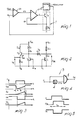
- the present invention relates to a circuit for sensing the waveform of the collector current in a transistor, in particular the switching transistor of a regulated power supply operating in current mode.
- a power supply of this type is shown in figure 1, corresponding to the device UC 1842 or UC 1846 manufactured by SGS Microelectronics.
- the power supply comprises a dual loop including an error amplifier EA which compares the regulated voltage V O with an externally fed reference voltage V REF and generates an error signal ES.
- a comparator CP is provided downstream the error amplifier EA in order to compare the error signal ES, which is fed to the non-inverting input of the comparator CP, to a saw-tooth signal RA which is proportional to the saw tooth current which flows through the collector of the switching transistor T S .
- Said saw-tooth signal RA generated by a sensing resistor R S connected between the emitter of the switching transistor T S and the ground, is fed to the inverting input of the comparator thus forming a feedback loop.
- the comparator CP generates a switching signal indicated by the letter C.
- Block 2 connected to the collector of transistor T S , is a part of the regulated power supply and generates the regulated output voltage V O , but is not shown in detail since it is well known in the art and not necessary for the comprehension of the present invention.
- the dimensioning of the sensing resistor R S is rather difficult, since two opposite conditions must be satisfied, namely: - in order to keep the dissipated power as low as possible, the sensing resistor R S must have a low resistive value; - and on the other hand the resistance of said resistor R S must be kept relatively high in order to maximize the dynamic amplitude of the saw-tooth signal.
- Said article describes a FET sensor in which a portion of the cells of the source is used for current sensing purposes, monitoring the absorbed current without intersecting in series to the current load a high-power dissipation resistor.
- the aim of the present invention is to provide a current sensing circuit which can be easily implemented in various technologies, for example MOS technology or bipolar technology.
- a particular object of the present invention is to provide a sensing circuit generating a good dynamic saw-tooth signal fed through a feedback loop to the comparator which controls the switching transistor and nevertheless has low power dissipation.
- a further object of the invention is to provide a sensing circuit structure, of the kind used in integrated circuits, which can be implemented at low cost.
- the block indicated by the reference numeral 1 in figure 1 is replaced with the switching circuit illustrated in figure 2 which receives at a first input the switching signal C and at a second input a control signal C R generated by an inverting delay block 3, such as the one illustrated in figure 4.
- the switching signal C is generated by the comparator CP, as is known in the art.
- said switching signal C is delayed by the delay block 4, indicated by T a , while the inversion is completed by means of the NAND gate 5.
- the resulting control signal C R is inverted and has a falling edge delayed with respect to the leading edge of the switching signal C, as illustrated in figure 5.
- the delay block has a conventional structure and comprises, for example, resistor means and capacitor means, as is well known in the art.
- the control signal C R is used, together with switching signal C, for controlling the switching circuit illustrated in figure 2.
- a first supply voltage line V SS and a second supply voltage line V CC feed the switching circuit; said voltage lines V SS and V CC , defining reference potential lines, are not necessarily equal to one another.
- the switching transistor is here defined by a first transistor T1, which is preferably constituted by a power transistor and has a collector current I C ; said transistor is controlled by said switching signal C which is applied to its base.
- the collector of said first transistor T1 is connected, through an impedance Z C , to the second supply voltage line V CC and to the cathode of a diode D, while the emitter of said first transistor T1 is connected to the ground G defining a further reference potential line.
- the impedance Z C represents the block 2 of figure 1 if the switching circuit of figure 2 is used in a power supply of the type shown in figure 1, but may represent any load fed by the collector current of transistor T1.
- the switching circuit further comprises a second transistor T2 which defines a switch element and is controlled by the control signal C R applied to its base.
- the collector of the second transistor T2 is connected to the anode of said diode D, to a current source S which generates a constant current I p , and to the base of a third transistor T3 defining a transducing transistor.
- the emitter of said second transistor is connected to the ground.
- the current source S is fed by said first supply voltage line V SS which is also connected to the collector of the third transistor T3.
- the emitter of the third transistor is connected to the ground through resistor R.
- the first transistor T1 is on while the second transistor T2 is off and the third transistor T3 is on since it is not short-circuited by the second transistor.
- the voltage drop V P across the diode D is approximately equal to the base-emitter voltage drop V BE across said third transistor T3 so that the voltage drop V R across the resistor R (corresponding to signal RA of figure 1 to be fed to comparator CP) is consequently equal to the collector-emitter voltage drop across said first transistor T1.
- the pair of elements constituted by the third transistor T3 and by the diode D acts as a differential amplifier controlled by transistor T2 which switches off the differential amplifier when signal C R is high.
- the first transistor T1 switches off and the current source S is connected to ground through transistor T2, thus causing the third transistor T3 to switch off.
- the switching signal C and the control signal C R as illustrated in the diagram of figure 3, therefore allow to extract the waveform of the collector currents I C and I C3 .
- the falling edge of the signal C R must be delayed by the time T a with respect to the leading edge of the switching signal C, thus the third transistor T3 is switched off after the first transistor T1 is switched on.
- the power transistor T S in the conducting state has an equivalent resistance of 1 ⁇
- the resistor R S has a value of 1 ⁇ and the collector current I C is of 1 A
- the power dissipated by R S is 1 W
- the power dissipated by T S is also 1 W.
- resistor R has a value of 1 K ⁇
- V SS might be of the order of 10 V
- the current I P which is fed by the source S which feeds the third transistor T3 is of the order of 10 ⁇ A, while the NAND gate which feeds the signal C R also has a consumption in the range of a few mW. All the power consumption estimates approximately correspond to practical values.
- the power consumption of the circuit of figure 2 is in the range of 10 mW, and is therefore much lower than the one of block 1, while the dynamic excursion of the signals across R S and R is identical.
- the transistors may furthermore be replaced with equivalent switching means.
- the current sensing circuit of figure 2 may be applied to any device including a controlled transistor such as T1, the collector current of which should be controlled with high dynamics and low dissipation and is not limited to regulated power supply as shown in figure 1.
- a controlled transistor such as T1
Landscapes
- Measurement Of Current Or Voltage (AREA)
- Electronic Switches (AREA)
- Dc-Dc Converters (AREA)
Abstract
Description
- The present invention relates to a circuit for sensing the waveform of the collector current in a transistor, in particular the switching transistor of a regulated power supply operating in current mode.
- The use of power switching transistors in circuits of the so-called current-mode type, in which the waveform of the collector current of the switching transistor is controlled by resistor means, is well known in the art.
- A power supply of this type is shown in figure 1, corresponding to the device UC 1842 or UC 1846 manufactured by SGS Microelectronics. As visible, the power supply comprises a dual loop including an error amplifier EA which compares the regulated voltage VO with an externally fed reference voltage VREF and generates an error signal ES. A comparator CP is provided downstream the error amplifier EA in order to compare the error signal ES, which is fed to the non-inverting input of the comparator CP, to a saw-tooth signal RA which is proportional to the saw tooth current which flows through the collector of the switching transistor TS. Said saw-tooth signal RA, generated by a sensing resistor RS connected between the emitter of the switching transistor TS and the ground, is fed to the inverting input of the comparator thus forming a feedback loop. The comparator CP generates a switching signal indicated by the letter C.
- Block 2, connected to the collector of transistor TS, is a part of the regulated power supply and generates the regulated output voltage VO, but is not shown in detail since it is well known in the art and not necessary for the comprehension of the present invention.
- In this known device, the dimensioning of the sensing resistor RS is rather difficult, since two opposite conditions must be satisfied, namely:
- in order to keep the dissipated power as low as possible, the sensing resistor RS must have a low resistive value;
- and on the other hand the resistance of said resistor RS must be kept relatively high in order to maximize the dynamic amplitude of the saw-tooth signal. - This in turn facilitates the comparison of the saw-tooth signal RA with the error signal ES by the comparator CP.
- A solution to the above mentioned problem is disclosed in the article "Current Mirror FET's cut cost and sensing losses" (Garry Fay, in EDN, September 4, 1986, pages 193-200).
- Said article describes a FET sensor in which a portion of the cells of the source is used for current sensing purposes, monitoring the absorbed current without intersecting in series to the current load a high-power dissipation resistor.
- However, though it solves the conflicting problems of the circuit illustrated in figure 1, the previously described solution can be implemented exclusively in MOS technology and cannot be made in bipolar technology.
- In view of the above described situation, the aim of the present invention is to provide a current sensing circuit which can be easily implemented in various technologies, for example MOS technology or bipolar technology.
- Within the above described aim, a particular object of the present invention is to provide a sensing circuit generating a good dynamic saw-tooth signal fed through a feedback loop to the comparator which controls the switching transistor and nevertheless has low power dissipation.
- A further object of the invention is to provide a sensing circuit structure, of the kind used in integrated circuits, which can be implemented at low cost.
- The above described aim and objects, as well as others which will become apparent hereinafter, are achieved by the circuit as defined in claim 1.
- The characteristics and advantages will become apparent from the following description of the preferred but not exclusive embodiment, illustrated only by way of non-limitative example in the accompanying drawings, wherein:
- figure 1 is a block diagram of the prior art regulated power supply including a switching transistor and a sensing resistor;
- figure 2 is a general diagram of the switching circuit according to the invention which replaces the switching transistor and the sensing resistor of figure 1;
- figure 3 is a waveform diagram of some electrical signals generated by the switching circuit of figure 2;
- figure 4 is a view of an embodiment of an inverting and delay block generating a control signal CR fed to the circuit of figure 2; and
- figure 5 is a time plot of the signals C and CR.
- According to the invention, the block indicated by the reference numeral 1 in figure 1 is replaced with the switching circuit illustrated in figure 2 which receives at a first input the switching signal C and at a second input a control signal CR generated by an inverting
delay block 3, such as the one illustrated in figure 4. - The switching signal C is generated by the comparator CP, as is known in the art.
- In the circuit of figure 4, said switching signal C is delayed by the
delay block 4, indicated by Ta, while the inversion is completed by means of the NAND gate 5. In particular, the resulting control signal CR is inverted and has a falling edge delayed with respect to the leading edge of the switching signal C, as illustrated in figure 5. The delay block has a conventional structure and comprises, for example, resistor means and capacitor means, as is well known in the art. - The control signal CR is used, together with switching signal C, for controlling the switching circuit illustrated in figure 2.
- A first supply voltage line VSS and a second supply voltage line VCC feed the switching circuit; said voltage lines VSS and VCC, defining reference potential lines, are not necessarily equal to one another. The switching transistor is here defined by a first transistor T₁, which is preferably constituted by a power transistor and has a collector current IC; said transistor is controlled by said switching signal C which is applied to its base.
- The collector of said first transistor T₁ is connected, through an impedance ZC, to the second supply voltage line VCC and to the cathode of a diode D, while the emitter of said first transistor T₁ is connected to the ground G defining a further reference potential line. The impedance ZC represents the block 2 of figure 1 if the switching circuit of figure 2 is used in a power supply of the type shown in figure 1, but may represent any load fed by the collector current of transistor T₁.
- The switching circuit further comprises a second transistor T₂ which defines a switch element and is controlled by the control signal CR applied to its base. As can be seen, the collector of the second transistor T₂ is connected to the anode of said diode D, to a current source S which generates a constant current Ip, and to the base of a third transistor T₃ defining a transducing transistor. The emitter of said second transistor is connected to the ground.
- The current source S is fed by said first supply voltage line VSS which is also connected to the collector of the third transistor T₃. The emitter of the third transistor is connected to the ground through resistor R.
- It is evident that while the switching signal C is active and the control signal CR is low, the first transistor T₁ is on while the second transistor T₂ is off and the third transistor T₃ is on since it is not short-circuited by the second transistor. The voltage drop VP across the diode D is approximately equal to the base-emitter voltage drop VBE across said third transistor T₃ so that the voltage drop VR across the resistor R (corresponding to signal RA of figure 1 to be fed to comparator CP) is consequently equal to the collector-emitter voltage drop across said first transistor T₁. In practice, the pair of elements constituted by the third transistor T₃ and by the diode D acts as a differential amplifier controlled by transistor T₂ which switches off the differential amplifier when signal CR is high. If RON designates the equivalent conducting resistivity of the first transistor and IC indicates the collector current thereof, since:
VCE = RON . IC,
VR = VCE is consequently a linear function of said collector current IC, and IC3, i.e. the collector current of said third transistor T₃, is also a linear function of the collector current IC. - When the second transistor is switched on by the control signal CR and the switching signal C becomes inactive, the first transistor T₁ switches off and the current source S is connected to ground through transistor T₂, thus causing the third transistor T₃ to switch off.
- The switching signal C and the control signal CR, as illustrated in the diagram of figure 3, therefore allow to extract the waveform of the collector currents IC and IC3.
- According to the switching time of the first power transistor T₁, the falling edge of the signal CR must be delayed by the time Ta with respect to the leading edge of the switching signal C, thus the third transistor T₃ is switched off after the first transistor T₁ is switched on.
- A simple estimate calculation which compares the power dissipated on the resistor RS illustrated in figure 1 to the power dissipated by the resistor R of the present invention shows that the invention achieves its aim.
- With reference to figure 1, if the power transistor TS in the conducting state has an equivalent resistance of 1 Ω, the resistor RS has a value of 1 Ω and the collector current IC is of 1 A, the power dissipated by RS is 1 W, while the power dissipated by TS is also 1 W.
- With reference to the present invention and to figure 2, if resistor R has a value of 1 KΩ, and assuming the first transistor T₁ has characteristics which are similar to those of TS, since VCE = VR, consequently IC3 is 1 mA.
- As VSS might be of the order of 10 V, the power dissipation of the third transistor T₃ is about V x 1 mA = 10 mW. The current IP which is fed by the source S which feeds the third transistor T₃ is of the order of 10 µA, while the NAND gate which feeds the signal CR also has a consumption in the range of a few mW. All the power consumption estimates approximately correspond to practical values.
- With the above values, the power consumption of the circuit of figure 2 is in the range of 10 mW, and is therefore much lower than the one of block 1, while the dynamic excursion of the signals across RS and R is identical.
- The increase in the number of components employed with respect to the known art is completely compensated by the power savings.
- The invention thus conceived is susceptible to numerous modifications and variations, all of which are within the scope of the inventive concept. In particular, it should be noted that though a specific embodiment employing bipolar technology has been illustrated, an implementation in MOS technology is also possible.
- The transistors may furthermore be replaced with equivalent switching means.
- Furthermore, the current sensing circuit of figure 2 may be applied to any device including a controlled transistor such as T₁, the collector current of which should be controlled with high dynamics and low dissipation and is not limited to regulated power supply as shown in figure 1.
- Where technical features mentioned in any claim are followed by reference signs, those reference signs have been included for the sole purpose of increasing the intelligibility of the claims and accordingly such reference signs do not have any limiting effect on the scope of each element identified by way of example by such reference signs.
Claims (9)
Applications Claiming Priority (2)
| Application Number | Priority Date | Filing Date | Title |
|---|---|---|---|
| IT8821955A IT1226938B (en) | 1988-09-15 | 1988-09-15 | CIRCUIT FOR DETECTION OF CURRENT WAVE FORM IN A TRANSISTOR |
| IT2195588 | 1988-09-15 |
Publications (3)
| Publication Number | Publication Date |
|---|---|
| EP0359171A2 true EP0359171A2 (en) | 1990-03-21 |
| EP0359171A3 EP0359171A3 (en) | 1991-08-07 |
| EP0359171B1 EP0359171B1 (en) | 1996-04-03 |
Family
ID=11189361
Family Applications (1)
| Application Number | Title | Priority Date | Filing Date |
|---|---|---|---|
| EP89116763A Expired - Lifetime EP0359171B1 (en) | 1988-09-15 | 1989-09-11 | Circuit for sensing the transistor current waveform |
Country Status (5)
| Country | Link |
|---|---|
| US (1) | US4929883A (en) |
| EP (1) | EP0359171B1 (en) |
| JP (1) | JPH02154159A (en) |
| DE (1) | DE68926138T2 (en) |
| IT (1) | IT1226938B (en) |
Families Citing this family (9)
| Publication number | Priority date | Publication date | Assignee | Title |
|---|---|---|---|---|
| US5247240A (en) * | 1990-07-25 | 1993-09-21 | Power Trends | Miniaturized switching power supply with circuit for unidirectional suppression of leading spike |
| US5164659A (en) * | 1991-08-29 | 1992-11-17 | Warren Schultz | Switching circuit |
| JP3337079B2 (en) * | 1991-11-26 | 2002-10-21 | ローム株式会社 | Power circuit |
| US5319303A (en) * | 1992-02-12 | 1994-06-07 | Sony/Tektronix Corporation | Current source circuit |
| JP3523718B2 (en) * | 1995-02-06 | 2004-04-26 | 株式会社ルネサステクノロジ | Semiconductor device |
| US5760571A (en) * | 1995-08-16 | 1998-06-02 | Signal Restoration Technologies I Limited Partnership | Power supply damping circuit and method |
| FR2767589B1 (en) * | 1997-08-21 | 2000-07-21 | Sgs Thomson Microelectronics | “RESET” TYPE SUPPLY VOLTAGE MONITORING DEVICE |
| JPH11224131A (en) * | 1998-02-04 | 1999-08-17 | Seiko Instruments Inc | Voltage regulator |
| US8238127B1 (en) * | 2007-10-31 | 2012-08-07 | Sadwick Laurence P | Method and apparatus for supplying and switching power |
Family Cites Families (7)
| Publication number | Priority date | Publication date | Assignee | Title |
|---|---|---|---|---|
| NL177858C (en) * | 1976-03-31 | 1985-12-02 | Philips Nv | CIRCUIT FOR SUPPLYING A PRE-DETERMINED CURRENT TO A TAX. |
| US4072890A (en) * | 1976-10-18 | 1978-02-07 | Honeywell Inc. | Voltage regulator |
| US4107596A (en) * | 1976-10-21 | 1978-08-15 | The Singer Company | Efficient bidirectional power converter for portable data gathering apparatus |
| US4291357A (en) * | 1979-12-27 | 1981-09-22 | International Business Machines Corp. | Short circuit protection circuit |
| US4339707A (en) * | 1980-12-24 | 1982-07-13 | Honeywell Inc. | Band gap voltage regulator |
| JPH0690656B2 (en) * | 1985-01-24 | 1994-11-14 | ソニー株式会社 | Reference voltage formation circuit |
| FR2588431B1 (en) * | 1985-10-08 | 1987-11-20 | Radiotechnique | VOLTAGE REGULATOR CIRCUIT |
-
1988
- 1988-09-15 IT IT8821955A patent/IT1226938B/en active
-
1989
- 1989-09-11 DE DE68926138T patent/DE68926138T2/en not_active Expired - Fee Related
- 1989-09-11 EP EP89116763A patent/EP0359171B1/en not_active Expired - Lifetime
- 1989-09-13 US US07/406,500 patent/US4929883A/en not_active Expired - Lifetime
- 1989-09-14 JP JP1239757A patent/JPH02154159A/en active Pending
Also Published As
| Publication number | Publication date |
|---|---|
| JPH02154159A (en) | 1990-06-13 |
| DE68926138T2 (en) | 1996-12-12 |
| EP0359171A3 (en) | 1991-08-07 |
| DE68926138D1 (en) | 1996-05-09 |
| IT8821955A0 (en) | 1988-09-15 |
| IT1226938B (en) | 1991-02-22 |
| US4929883A (en) | 1990-05-29 |
| EP0359171B1 (en) | 1996-04-03 |
Similar Documents
| Publication | Publication Date | Title |
|---|---|---|
| US4906913A (en) | Low dropout voltage regulator with quiescent current reduction | |
| US4338646A (en) | Current limiting circuit | |
| US5317254A (en) | Bipolar power supply | |
| US4384219A (en) | Voltage comparator hysteresis control circuit | |
| EP0359171B1 (en) | Circuit for sensing the transistor current waveform | |
| KR930009191B1 (en) | Clamp circuit | |
| JPS6162321A (en) | Battery energy saving circuit | |
| US6957278B1 (en) | Reference -switch hysteresis for comparator applications | |
| US4831323A (en) | Voltage limiting circuit | |
| EP0238803A1 (en) | Stabilized power-supply circuit | |
| TW353165B (en) | Temperature detecting circuit | |
| JPS61169020A (en) | Variable speed up circuit for ttl type gate | |
| US4801825A (en) | Three level state logic circuit having improved high voltage to high output impedance transition | |
| EP0620513B1 (en) | Balanced voltage-to-current converter with quiescent current control | |
| US5617056A (en) | Base current compensation circuit | |
| EP0157447A1 (en) | Differential amplifier | |
| US4567388A (en) | Clamp circuit | |
| EP0343731A2 (en) | Unity-gain current-limiting circuit | |
| KR0167563B1 (en) | Fractional load current detector | |
| EP0410764A2 (en) | Comparator circuit | |
| JP3355197B2 (en) | Digital output circuit | |
| JPH02177724A (en) | output buffer circuit | |
| JP2001042954A (en) | Regulator circuit | |
| US5973513A (en) | Integrated circuit arrangement with an open-collector transistor designed as npn transistor | |
| JPH0714130B2 (en) | Monolithically integrated protection circuit device for fault voltage generated in signal line |
Legal Events
| Date | Code | Title | Description |
|---|---|---|---|
| PUAI | Public reference made under article 153(3) epc to a published international application that has entered the european phase |
Free format text: ORIGINAL CODE: 0009012 |
|
| AK | Designated contracting states |
Kind code of ref document: A2 Designated state(s): DE FR GB NL SE |
|
| PUAL | Search report despatched |
Free format text: ORIGINAL CODE: 0009013 |
|
| AK | Designated contracting states |
Kind code of ref document: A3 Designated state(s): DE FR GB NL SE |
|
| 17P | Request for examination filed |
Effective date: 19920117 |
|
| 17Q | First examination report despatched |
Effective date: 19931203 |
|
| GRAA | (expected) grant |
Free format text: ORIGINAL CODE: 0009210 |
|
| AK | Designated contracting states |
Kind code of ref document: B1 Designated state(s): DE FR GB NL SE |
|
| PG25 | Lapsed in a contracting state [announced via postgrant information from national office to epo] |
Ref country code: NL Free format text: LAPSE BECAUSE OF FAILURE TO SUBMIT A TRANSLATION OF THE DESCRIPTION OR TO PAY THE FEE WITHIN THE PRESCRIBED TIME-LIMIT Effective date: 19960403 |
|
| REF | Corresponds to: |
Ref document number: 68926138 Country of ref document: DE Date of ref document: 19960509 |
|
| PG25 | Lapsed in a contracting state [announced via postgrant information from national office to epo] |
Ref country code: SE Effective date: 19960703 |
|
| ET | Fr: translation filed | ||
| NLV1 | Nl: lapsed or annulled due to failure to fulfill the requirements of art. 29p and 29m of the patents act | ||
| PLBE | No opposition filed within time limit |
Free format text: ORIGINAL CODE: 0009261 |
|
| STAA | Information on the status of an ep patent application or granted ep patent |
Free format text: STATUS: NO OPPOSITION FILED WITHIN TIME LIMIT |
|
| 26N | No opposition filed | ||
| REG | Reference to a national code |
Ref country code: FR Ref legal event code: D6 |
|
| REG | Reference to a national code |
Ref country code: GB Ref legal event code: IF02 |
|
| PGFP | Annual fee paid to national office [announced via postgrant information from national office to epo] |
Ref country code: FR Payment date: 20020910 Year of fee payment: 14 |
|
| PGFP | Annual fee paid to national office [announced via postgrant information from national office to epo] |
Ref country code: GB Payment date: 20020911 Year of fee payment: 14 |
|
| PGFP | Annual fee paid to national office [announced via postgrant information from national office to epo] |
Ref country code: DE Payment date: 20020918 Year of fee payment: 14 |
|
| PG25 | Lapsed in a contracting state [announced via postgrant information from national office to epo] |
Ref country code: GB Free format text: LAPSE BECAUSE OF NON-PAYMENT OF DUE FEES Effective date: 20030911 |
|
| PG25 | Lapsed in a contracting state [announced via postgrant information from national office to epo] |
Ref country code: DE Free format text: LAPSE BECAUSE OF NON-PAYMENT OF DUE FEES Effective date: 20040401 |
|
| GBPC | Gb: european patent ceased through non-payment of renewal fee |
Effective date: 20030911 |
|
| PG25 | Lapsed in a contracting state [announced via postgrant information from national office to epo] |
Ref country code: FR Free format text: LAPSE BECAUSE OF NON-PAYMENT OF DUE FEES Effective date: 20040528 |
|
| REG | Reference to a national code |
Ref country code: FR Ref legal event code: ST |