EP0356108A2 - Sourcefolger-Feldeffektlogik (SFFL), geeignet für III-V Technologien - Google Patents
Sourcefolger-Feldeffektlogik (SFFL), geeignet für III-V Technologien Download PDFInfo
- Publication number
- EP0356108A2 EP0356108A2 EP89308259A EP89308259A EP0356108A2 EP 0356108 A2 EP0356108 A2 EP 0356108A2 EP 89308259 A EP89308259 A EP 89308259A EP 89308259 A EP89308259 A EP 89308259A EP 0356108 A2 EP0356108 A2 EP 0356108A2
- Authority
- EP
- European Patent Office
- Prior art keywords
- logic
- gate
- stage
- output
- logic gate
- Prior art date
- Legal status (The legal status is an assumption and is not a legal conclusion. Google has not performed a legal analysis and makes no representation as to the accuracy of the status listed.)
- Withdrawn
Links
Images

Classifications
-
- H—ELECTRICITY
- H03—ELECTRONIC CIRCUITRY
- H03K—PULSE TECHNIQUE
- H03K19/00—Logic circuits, i.e. having at least two inputs acting on one output; Inverting circuits
- H03K19/02—Logic circuits, i.e. having at least two inputs acting on one output; Inverting circuits using specified components
- H03K19/08—Logic circuits, i.e. having at least two inputs acting on one output; Inverting circuits using specified components using semiconductor devices
- H03K19/094—Logic circuits, i.e. having at least two inputs acting on one output; Inverting circuits using specified components using semiconductor devices using field-effect transistors
- H03K19/0952—Logic circuits, i.e. having at least two inputs acting on one output; Inverting circuits using specified components using semiconductor devices using field-effect transistors using Schottky type FET MESFET
Definitions
- the present invention relates to logic gates generally and, more particularly, to logic gates integratable with III-V technologies such as in Gallium Arsenide (GaAs) integrated circuits.
- GaAs Gallium Arsenide
- Gallium Arsenide has long been recognized as material which could be used to integrate high-speed logic circuitry.
- conventional logic circuits i.e. those designed for integration into silicon, are not readily adaptable for integration into GaAs or other III-V materials such as Indium Phosphide. Consequently, several types of digital logic families were developed for use in GaAs integrated circuits.
- An exemplary common logic family is Direct Coupled FET Logic (DCFL).
- DCFL is a fast, relatively low power logic family but has small logic level voltage swings (typically 0.6 volts), resulting in small noise margins.
- VLSI Very Large Scale Integrated Circuits
- the power dissipation of a logic gate becomes a major concern while still providing high speed.
- the number of gates on a silicon VLSI chip using emitter-coupled logic is usually limited by the power dissipation of the chip. Consequently, for a GaAs VLSI chip, the most frequently utilized logic family is DCFL due to the relatively low power dissipation per DCFL gate.
- the small noise margins of DCFL typically 0.2 volts
- small logic level voltage swings typically 0.6 volts
- III-V materials such as Gallium Arsenide or Indium Phosphide.
- a further object of the invention is to provide a logic family tolerant of device parametric variation with wide noise margins for use in high density VLSI chips and gate arrays without sacrificing speed or power dissipation.
- a logic gate with an input stage and a buffer stage, the input stage including a logic stage responsive to logic signal inputs, for performing the required logic function.
- the logic stage has first and second output nodes and at least one enhancement FET per logic signal input.
- a first depletion FET adapted to form a current source and disposed between the first output node of the logic stage and a first power source, forms a pull-up load for the logic stage.
- a second depletion FET adapted to form a current sink and disposed between the second output node of the logic stage and a second power source, forms a pull-down load for the logic stage.
- the buffer stage has an enhancement FET, with a gate terminal coupling to the second output node of the logic stage, a first output terminal coupling to the second power source and a second output terminal coupling to the output node of the logic gate to pull-down the voltage thereon.
- the buffer stage includes alternative combinations of FETs and diodes to pull-up the voltage on the output node of the logic gate.
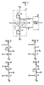
- a novel logic gate 10, suitable for integration to a III-V type of compound semiconductor integrated circuits, consists of an input stage 11 and a buffer stage 20 as shown in FIG. 1.
- the input stage 11 is shown in schematic form with the buffer stage 20 shown as a block. Details of different implementations of the buffer stage 20 will be given in more detail below in connection with FIGs. 2 through 8, but it is sufficient to state here that buffer 20 provides sufficient drive capability for the logic gate 10 to drive multiple logic gates (not shown) coupled to output node V0.
- Input stage 11 receives logic signals on a predetermined number of inputs, an exemplary two are shown here as logical inputs A, B. As will be explained in greater detail below, intermediate output nodes I, N have thereon the output of the input stage 11.
- Buffer 20 couples the signals on nodes I, N to output node V0 of the logic gate 10.
- the transistors shown in the given embodiments consist of enhancement and depletion field-effect transistors, referred to here as EFETs and DFETs, respectively. More particularly, the EFETs and DFETs are transistors implemented as N channel FETs in a III-V compound semiconductor technology, such as gallium arsenide (GaAs) or indium phosphide (InP) compounds.
- GaAs gallium arsenide
- InP indium phosphide
- the structure of the EFETs and DFETs either have metal gates, commonly referred to as MESFETs, or diffused gates, commonly referred to as JFETs, or, preferably, a heterojunction FET, commonly referred to as HFETs modulation-doped FETs (MODFETs) or high electron mobility transistor (HEMT).
- the EFETs are normally off devices, typically requiring approximately +0.2 volts between the gate and source terminals thereof to bring them into a conducting state.
- DFETs are normally on devices requiring a reverse voltage of approximately -0.6 volts between the gate and source terminals thereof to substantially turn-off the devices.
- MOSFETs metal-oxide-semiconductor FETs
- III-V technology metal-oxide-semiconductor FETs
- the FETs shown herein can be MOSFETs.
- all FETs shown are N channel devices, P channel devices can be substituted with a corresponding change in polarity of the power sources V DD and V SS .
- the input stage 11 of logic gate 10 has a logic stage 12 consisting of at least one EFET 13 with common source and drain terminals. Individual gate terminals of the EFETs 13 couple to corresponding logic input terminals A, B to logically OR logic signals thereon. It is understood that instead of, or in addition to, paralleling EFETs 13, the EFETs 13 could be disposed serially, or with multiple gate terminals per EFET 13, to provide a logical AND function. Similarly, DFETs can be substituted for the EFETs in serial or parallel combination to perform the desired logic function.
- DFET 15 The common drain terminals of EFETs 13 coupled to a first intermediate output node I of the input stage.
- DFET 15 is adapted to operate as a current source by having the gate and source terminals thereof coupled together and the drain terminal thereof coupled to V DD , the most positive power source, typically 2.0 volts.
- DFET 15 thereby acts as a passive load by pulling up the voltage on node I to V DD .
- V DD the most positive power source
- DFET 16 is adapted to operate as a current sink by having the gate and source terminals thereof coupled to V SS , the most negative supply voltage, typically at ground or zero volts.
- the drain terminal of DFET 16 couples to the common source terminals of the EFETs 13 of the logic stage 12 and to a second intermediate output terminal N of the input stage 11.
- DFET 16 thereby acts as a passive load by pulling down the voltage on node N to V SS .
- N, I are the logical inverse of each other; as shown, the N output represents the logical OR of the inputs A, B and the I output represents the logical NOR of the inputs A, B.
- N output represents the logical OR of the inputs A, B
- I output represents the logical NOR of the inputs A, B.
- FIGs. 2 through 8 Alternative buffer stages 20 of the logic gate 10 (FIG. 1) are shown in FIGs. 2 through 8.
- an EFET 21 is shown having a gate terminal coupled to the second intermediate output terminal N of the input stage 11 (FIG. 1) and the source thereof coupled to V SS .
- the drain EFET 21 couples to the output terminal V0 of the buffer, also the output terminal of the logic gate 10 (FIG. 1).
- EFET 21 serves as a pull-down to the output node V0.
- the buffer stages 20 shown in FIGs. 2 - 8 are best described by way of example. As stated above, all buffers are shown having EFET 21 as the pull-down for the output node V0. The remaining circuitry serves as a pull-up of the output node V0, each type having a different advantage in speed or power dissipation.
- EFET 21 serves as the pull-down for the output node V0.
- DFET 22 in FIG. 2 pulls up the voltage on node V0 when node I is "high" and EFET 21 is off.
- schottky diode 23 pulls up the output node V0 when node I is high.
- EFET 24, shown here in a diode configuration also pulls up node V0.
- the DFET 22 of FIG. 2 serves as a current limiter, while the diode 23 and EFET 24 of FIG. 3 and FIG.
- the transient current flow results from the delay in EFET 21 discharging node V0 in response to node N going "high” (and, therefore, node I going “low”). However, diode 23 (EFET 24) reverse biases inhibiting the flow of transient current from node V0 to node I.
- EFET 24 reverse biases inhibiting the flow of transient current from node V0 to node I.
- Using these types of buffers with the input stage 11 of FIG. 1 results in a logic gate 10 having an average delay of 120 picoseconds.
- the average power dissipation of the logic gate 10 when using the buffer stages shown in FIGs. 2 and 4 is approximately 430 microwatts, while the average power dissipation is approximately 350 microwatts when using the buffer stage 20 of FIG. 3.
- the buffer 20 of FIG. 5 consists of a DFET 25, arranged as a current source with the gate and source terminals thereof coupling to the output node V0 and the drain terminal thereof coupling to V DD .
- DFET 25 then acts as a passive load to EFET 21 to pull-up the voltage on the output node V0. This results in a logic gate 10 having an average propagation delay of 130 picoseconds and an average power dissipation of approximately 700 microwatts.
- the buffer stage 20 of FIG. 6 is a combination of the buffers 20 in FIGs. 3 and 5.
- DFET 26, corresponding to DFET 25 in FIG. 5, is arranged as a current source to provide a passive load to EFET 21 to pull-up the voltage on the output node V0.
- schottky diode 27, corresponding to diode 23 in FIG. 3 assists in speeding up the transition of the output voltage on output node V0 from a logic "low” to logic "high” by recognizing that the voltage on node I changes before the voltage on the output node V0 due to propagation through delay of EFET 21.
- the logic gate 10 (FIG. 1) using this buffer would have an average propagation delay of 96 picoseconds and an average power dissipation of 650 microwatts.
- a diode connected EFET (not shown) can be substituted for the schottky diode 27.
- Buffer stage 20 of FIG. 7 has a DFET 28 arranged as a voltage follower (source follower) of the voltage on node I.
- the source terminal of DFET 28 couples to the output node V0 via schottky diode 29 to drop the voltage on the source terminal of DFET 28 to a lower voltage.
- the reduction in voltage results in better noise margins for the logical "zero" voltage level to subsequent logic gates.
- the resulting average propagation delay is approximately 103 picoseconds with an approximate power dissipation of 520 microwatts for the logic gate 10 of FIG. 1.
- schottky diode 29 of FIG. 7 can be replaced with a diode-connected EFET (not shown) for a lower voltage drop than possible with a schottky diode.
- Buffer stage 20 of FIG. 8 utilizes an EFET 30 as a voltage follower of the voltage on node I instead of DFET 28 in FIG. 7.
- a diode-connected EFET 31 couples the source terminal of EFET 30 to the output terminal V0.
- EFET 31 drops the voltage on the source terminal of EFET 30 to a lower voltage.
- Resulting average propagation delay is approximately 98 picoseconds and the approximate power dissipation is 400 microwatts.
- Replacing the EFET 31 with schottky diode (not shown) does not significantly change the average propagation delay or power dissipation.
- the approximate threshold voltage of the logic gate 10 is determined by the sizes and turn-on voltages V t of the EFETs 13, DFET 16 (FIG. 1) and EFET 21 (FIGs. 2 - 8).
- threshold voltage of the logic gate we mean the input voltage on inputs A, B (FIG. 1) at which the logic voltage level on the output terminal V0 (FIGs. 2 -8) changes state.
- the approximate threshold voltage is given by: where V t13 is the turn-on voltage of EFETs 13, V t21 is the turn-on voltage of EFET 21,g m21 is the transconductance of EFET 21, W21 is the width of EFET 21 and I0 is the desired output current through node V0 (FIG. 1).
- V t13 and V t21 are 0.2 volts
- I0 is 200 microamperes
- g m21 is 150 microsiemens per micrometer
- W21 ranges from 8 to 12 micrometers
- n the threshold voltage of the logic gate 10 ranging from 0.5 to 0.8 volts.
- the propagation delay and power dissipation of the logic gate 10 (FIG. 1) using any of the buffer stages 20 in FIGs. 2-8, are, to an extent, controlled by the current supplied by DFET 15.
- the primary purpose of DFET 15 serves to limit the current through the gate terminal of EFET 21 (FIGs. 3 - 8) when the node N is logically "high", forward biasing the gate-source junction thereof.
- the current from DFET 15 also charges capacitive loading on all nodes in the logic gate 10. It is therefore understood that the higher the current allowed by DFET 15, the faster the logic gate 10 is by the faster charging of the capacitive loading but with higher power dissipation. Further, DFET 15 establishes the propagation delay of the gate 10 with minimal effect on the threshold voltage of gate 10.
Landscapes
- Engineering & Computer Science (AREA)
- Power Engineering (AREA)
- Physics & Mathematics (AREA)
- Computer Hardware Design (AREA)
- Computing Systems (AREA)
- General Engineering & Computer Science (AREA)
- Mathematical Physics (AREA)
- Logic Circuits (AREA)
Applications Claiming Priority (2)
| Application Number | Priority Date | Filing Date | Title |
|---|---|---|---|
| US07/235,862 US4885480A (en) | 1988-08-23 | 1988-08-23 | Source follower field-effect logic gate (SFFL) suitable for III-V technologies |
| US235862 | 1988-08-23 |
Publications (2)
| Publication Number | Publication Date |
|---|---|
| EP0356108A2 true EP0356108A2 (de) | 1990-02-28 |
| EP0356108A3 EP0356108A3 (de) | 1990-10-31 |
Family
ID=22887198
Family Applications (1)
| Application Number | Title | Priority Date | Filing Date |
|---|---|---|---|
| EP19890308259 Withdrawn EP0356108A3 (de) | 1988-08-23 | 1989-08-15 | Sourcefolger-Feldeffektlogik (SFFL), geeignet für III-V Technologien |
Country Status (3)
| Country | Link |
|---|---|
| US (1) | US4885480A (de) |
| EP (1) | EP0356108A3 (de) |
| JP (1) | JPH02216912A (de) |
Cited By (1)
| Publication number | Priority date | Publication date | Assignee | Title |
|---|---|---|---|---|
| FR2646740A1 (fr) * | 1989-05-08 | 1990-11-09 | Mitsubishi Electric Corp | Circuit logique a fonctionnement quasi complementaire |
Families Citing this family (7)
| Publication number | Priority date | Publication date | Assignee | Title |
|---|---|---|---|---|
| US5068553A (en) * | 1988-10-31 | 1991-11-26 | Texas Instruments Incorporated | Delay stage with reduced Vdd dependence |
| US5027007A (en) * | 1989-04-12 | 1991-06-25 | The Boeing Company | FFL/QFL FET logic circuits |
| US5077494A (en) * | 1989-08-21 | 1991-12-31 | Analog Devices, Inc. | Wide temperature range mesfet logic circuit |
| JP3643421B2 (ja) * | 1996-01-29 | 2005-04-27 | 富士通株式会社 | 出力回路 |
| US20050206439A1 (en) * | 2004-03-22 | 2005-09-22 | Triquint Semiconductor, Inc. | Low quiescent current radio frequency switch decoder |
| EP2264900B1 (de) * | 2009-06-17 | 2014-07-30 | Epcos AG | Inverter mit niedriger Stromstärke |
| CN105955390A (zh) * | 2016-07-01 | 2016-09-21 | 唯捷创芯(天津)电子技术股份有限公司 | 低压差线性稳压器模块、芯片及通信终端 |
Citations (2)
| Publication number | Priority date | Publication date | Assignee | Title |
|---|---|---|---|---|
| JPS60220617A (ja) * | 1984-04-17 | 1985-11-05 | Mitsubishi Electric Corp | レベルシフタ |
| EP0196391A2 (de) * | 1985-03-28 | 1986-10-08 | Kabushiki Kaisha Toshiba | Integrierte Schaltung mit einem Gallium-Arsenid-Gate-Array unter Verwendung von NAND-Gattern in direkt gekoppelter Feldeffekttransistorlogik |
Family Cites Families (12)
| Publication number | Priority date | Publication date | Assignee | Title |
|---|---|---|---|---|
| US4400636A (en) * | 1980-12-05 | 1983-08-23 | Ibm Corporation | Threshold voltage tolerant logic |
| US4405870A (en) * | 1980-12-10 | 1983-09-20 | Rockwell International Corporation | Schottky diode-diode field effect transistor logic |
| US4445051A (en) * | 1981-06-26 | 1984-04-24 | Burroughs Corporation | Field effect current mode logic gate |
| US4698524A (en) * | 1986-07-16 | 1987-10-06 | Honeywell Inc. | MESFET logic using integral diode level shifting |
| US4404480A (en) * | 1982-02-01 | 1983-09-13 | Sperry Corporation | High speed-low power gallium arsenide basic logic circuit |
| JPS5949020A (ja) * | 1982-09-13 | 1984-03-21 | Toshiba Corp | 論理回路 |
| US4590393A (en) * | 1983-06-13 | 1986-05-20 | Sperry Corporation | High density gallium arsenide source driven logic circuit |
| FR2552257B1 (fr) * | 1983-09-16 | 1985-10-31 | Labo Electronique Physique | Circuit decodeur pour memoire ram statique |
| US4713559A (en) * | 1985-04-29 | 1987-12-15 | Honeywell Inc. | Multiple input and multiple output or/and circuit |
| US4724342A (en) * | 1986-02-12 | 1988-02-09 | Hughes Aircraft Company | Push-pull DCFL driver circuit |
| US4725743A (en) * | 1986-04-25 | 1988-02-16 | International Business Machines Corporation | Two-stage digital logic circuits including an input switching stage and an output driving stage incorporating gallium arsenide FET devices |
| US4800303A (en) * | 1987-05-19 | 1989-01-24 | Gazelle Microcircuits, Inc. | TTL compatible output buffer |
-
1988
- 1988-08-23 US US07/235,862 patent/US4885480A/en not_active Expired - Lifetime
-
1989
- 1989-08-15 EP EP19890308259 patent/EP0356108A3/de not_active Withdrawn
- 1989-08-23 JP JP1215155A patent/JPH02216912A/ja active Pending
Patent Citations (2)
| Publication number | Priority date | Publication date | Assignee | Title |
|---|---|---|---|---|
| JPS60220617A (ja) * | 1984-04-17 | 1985-11-05 | Mitsubishi Electric Corp | レベルシフタ |
| EP0196391A2 (de) * | 1985-03-28 | 1986-10-08 | Kabushiki Kaisha Toshiba | Integrierte Schaltung mit einem Gallium-Arsenid-Gate-Array unter Verwendung von NAND-Gattern in direkt gekoppelter Feldeffekttransistorlogik |
Non-Patent Citations (1)
| Title |
|---|
| PATENT ABSTRACTS OF JAPAN, vol. 10, no. 75 (E-390)[2132], 25th March 1986; & JP-A-60 220 617 (MITSUBISHI DENKI K.K.) 05-11-1985 * |
Cited By (1)
| Publication number | Priority date | Publication date | Assignee | Title |
|---|---|---|---|---|
| FR2646740A1 (fr) * | 1989-05-08 | 1990-11-09 | Mitsubishi Electric Corp | Circuit logique a fonctionnement quasi complementaire |
Also Published As
| Publication number | Publication date |
|---|---|
| EP0356108A3 (de) | 1990-10-31 |
| US4885480A (en) | 1989-12-05 |
| JPH02216912A (ja) | 1990-08-29 |
Similar Documents
| Publication | Publication Date | Title |
|---|---|---|
| US4096398A (en) | MOS output buffer circuit with feedback | |
| EP0099100A1 (de) | Gateschaltung mit Feldeffekt- und Bipolartransistoren | |
| EP0075915B1 (de) | Logische Schaltung gespeist durch nur eine Spannung | |
| US4663543A (en) | Voltage level shifting depletion mode FET logical circuit | |
| US4724342A (en) | Push-pull DCFL driver circuit | |
| US4490632A (en) | Noninverting amplifier circuit for one propagation delay complex logic gates | |
| US4885480A (en) | Source follower field-effect logic gate (SFFL) suitable for III-V technologies | |
| US4713559A (en) | Multiple input and multiple output or/and circuit | |
| US4810905A (en) | Capacitor coupled push pull logic circuit | |
| US4931670A (en) | TTL and CMOS logic compatible GAAS logic family | |
| US4395645A (en) | Mosfet logic inverter buffer circuit for integrated circuits | |
| US4937474A (en) | Low power, high noise margin logic gates employing enhancement mode switching FETs | |
| EP0186940B1 (de) | Logisches Gatter mit "verdrahteter" UND-Funktion-Eingangsstufe unter Verwendung von Feldeffekttransistoren | |
| US4716311A (en) | Direct coupled FET logic with super buffer output stage | |
| US4639621A (en) | Gallium arsenide gate array integrated circuit including DCFL NAND gate | |
| EP0217072A1 (de) | Halbleitereinrichtung | |
| EP0320582A2 (de) | Bicmos-Treiberschaltung mit Submikron-Spannungsquelle auf dem IC | |
| EP0380095B1 (de) | Logische Schaltung | |
| US4418292A (en) | Logic gate having a noise immunity circuit | |
| US5661411A (en) | Feedback controlled load logic circuit | |
| US4704544A (en) | Complementary current mirror logic | |
| JPH09261038A (ja) | 論理回路 | |
| EP0170134B1 (de) | Schottky-Dioden und Feldeffekt-Transistoren verwendende Logikschaltung | |
| US5239212A (en) | Gate circuit of combined field-effect and bipolar transistors with an improved discharge arrangement | |
| US6111430A (en) | Circuit for interfacing a first type of logic circuit with a second type of logic circuit |
Legal Events
| Date | Code | Title | Description |
|---|---|---|---|
| PUAI | Public reference made under article 153(3) epc to a published international application that has entered the european phase |
Free format text: ORIGINAL CODE: 0009012 |
|
| AK | Designated contracting states |
Kind code of ref document: A2 Designated state(s): DE FR GB |
|
| PUAL | Search report despatched |
Free format text: ORIGINAL CODE: 0009013 |
|
| AK | Designated contracting states |
Kind code of ref document: A3 Designated state(s): DE FR GB |
|
| 17P | Request for examination filed |
Effective date: 19901212 |
|
| 17Q | First examination report despatched |
Effective date: 19920928 |
|
| STAA | Information on the status of an ep patent application or granted ep patent |
Free format text: STATUS: THE APPLICATION IS DEEMED TO BE WITHDRAWN |
|
| 18D | Application deemed to be withdrawn |
Effective date: 19930209 |