EP0356034A2 - Optischer Sensor - Google Patents
Optischer Sensor Download PDFInfo
- Publication number
- EP0356034A2 EP0356034A2 EP89307784A EP89307784A EP0356034A2 EP 0356034 A2 EP0356034 A2 EP 0356034A2 EP 89307784 A EP89307784 A EP 89307784A EP 89307784 A EP89307784 A EP 89307784A EP 0356034 A2 EP0356034 A2 EP 0356034A2
- Authority
- EP
- European Patent Office
- Prior art keywords
- light
- charge
- capacitors
- pulse source
- sensor
- Prior art date
- Legal status (The legal status is an assumption and is not a legal conclusion. Google has not performed a legal analysis and makes no representation as to the accuracy of the status listed.)
- Withdrawn
Links
Images
Classifications
-
- H—ELECTRICITY
- H04—ELECTRIC COMMUNICATION TECHNIQUE
- H04N—PICTORIAL COMMUNICATION, e.g. TELEVISION
- H04N23/00—Cameras or camera modules comprising electronic image sensors; Control thereof
- H04N23/56—Cameras or camera modules comprising electronic image sensors; Control thereof provided with illuminating means
-
- H—ELECTRICITY
- H04—ELECTRIC COMMUNICATION TECHNIQUE
- H04N—PICTORIAL COMMUNICATION, e.g. TELEVISION
- H04N25/00—Circuitry of solid-state image sensors [SSIS]; Control thereof
- H04N25/60—Noise processing, e.g. detecting, correcting, reducing or removing noise
- H04N25/63—Noise processing, e.g. detecting, correcting, reducing or removing noise applied to dark current
-
- H—ELECTRICITY
- H04—ELECTRIC COMMUNICATION TECHNIQUE
- H04N—PICTORIAL COMMUNICATION, e.g. TELEVISION
- H04N25/00—Circuitry of solid-state image sensors [SSIS]; Control thereof
- H04N25/70—SSIS architectures; Circuits associated therewith
- H04N25/701—Line sensors
Definitions
- This invention relates to an optical sensor, and in particular to an optical sensor comprising a plurality of light-sensitive members each having an individually associated capacitor which is charged with a current dependent upon the incident light sensed by the associated light-sensitive member.
- each capacitor receives a charge which is dependent upon the light incident on the associated light-sensitive member and the time over which such charge is accumulated.
- Read out by the converter serves to 'flush' the capacitors, removing the charge thereon, whereafter the cycle of operation of the sensor is repeated.
- a difficulty that arises with such sensors is that light-sensitive members, for example light-sensitive diodes, generally exhibit some leakage current, referred to as 'dark current', which results in a charge on the associated capacitor in addition to that derived from the incident light.
- 'dark current' Such leakage current increases rapidly with increase in the ambient temperature, and thus the dark current charge becomes significant at elevated temperature operation of a sensor or if long charge accumulation periods are used. Thus, it can happen that a charge resulting from dark current saturates the sensor and swamps the required output signal of the sensor.
- Such difficulties limit the maximum operation temperature of known sensors, this in turn limiting their areas of use.
- an optical sensor comprising a plurality of light-sensitive members each having an individually associated capacitor which is charged with a current dependent upon the incident light sensed by the associated light-sensitive member; a light pulse source providing light pulses from which said incident light is derived; and a control pulse source providing pairs of consecutive pulses sandwiching the light pulses from the light pulse source, the first of which serves to discharge each capacitor to a reference level prior to issue of a pulse by said light pulse source and the second of which serves to effect read out from the capacitors of the charge thereon deriving from incident light from the preceding light pulse from the light pulse source.
- the first pulse of each pair from the control pulse source serves to clear the capacitors of any charge resulting from dark current in the period following the preceding read out from the capacitors, while the second pulse of each pair serves to effect read out of the charge on the capacitors resulting from incident light on the associated light-sensitive member, derived from the light pulse from the light pulse source, thereby ensuring the required output from the sensor is not swamped by charge on the capacitors resulting from dark current.
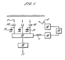
- the senor comprises a linear array of light-sensitive diodes 10 each arranged to charge an associated capacitor 11.
- the diodes 10 receive incident light I derived from light pulses 2 from a light pulse source 12 controlled by a timer 13.
- the timer 13 also controls a control pulse generator 14 which provides control pulses 1 to an analogue shift register 15 to which the charges on the capacitors 11 are transferred.
- the register 15 is read out by a charge-to-current or charge-to-voltage converter 16 which provides the output signal 17 of the sensor.
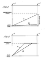
- FIG. 2 this illustrates operation of a known optical sensor utilising continuous rather than pulse illumination from which detected incident light is derived.
- a control pulse 1 by a control pulse source the capacitors of the sensor commence to charge, the total charge being a combination of that deriving from the incident light on the light-sensitive members and that deriving from the leakage current of the members.
- Line A shows this combined charge
- line B shows the leakage current charge.
- the combined charge (line A) does not result in saturation of the capacitors before issue of the next control pulse 1, at which the charge on the capacitors is read out to give the required output signal from the sensor, the capacitors being discharged by this action.
- the charge resulting from leakage current causes a shift in the level of the output signal and can be compensated for on interpretation of the output signal.
- FIG 3 this is similar to Figure 2, but illustrates operation of the known sensor at high ambient temperatures. As shown, during such operation the charge received by the capacitors deriving from the incident light and the leakage current, or even that resulting from leakage current alone, can result in the capacitors being charged to their saturation level thus making it impossible to derive the required output signal from the signal.
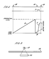
- the light pulse source provides light pulses 2 from which the incident light sensed by the light-sensitive members is derived.
- the control pulse source provides pairs of control pulses 1A and 1B timed to just precede and succeed a pulse 2 from the light pulse source.
- the first control pulse 1A of each pair serves to discharge the capacitors thus clearing them of any charge deriving from leakage current (line B) in the associated light-sensitive members.
- the capacitors commence to charge again, first from leakage current (line B), and then, on issue of the light pulse 2, in dependence upon the incident light on the associated light-sensitive members deriving from the light pulse 2.
- On occurence of control pulse 1B the charge on the capacitors is read out to provide the required output signal, as described for Figures 2 and 3, it being ensured that by this time the charge on the capacitors has not reached saturation level, as clearly shown in Figure 4.
- the sensor of the invention is particularly suitable for use in reading an optical digitiser as shown in Figure 5, comprising a digitiser disc 18, a flash illumination light source 19, and an optical sensor 20.
- the sensor of the invention ensures that any leakage current of the light-sensitive members during such intervals would not prevent satisfactory operation of the sensor. Such operation also minimises the average power consumed by the sensor enabling a high peak power for the illuminating pulses. Further, in view of its decreased temperature sensitivity the sensor of the invention can be used in aircraft where ambient temperatures in excess of 100°C can be experienced.
- the light pulse source 19 provides a 40 ms pulse every 4 ms, thus giving a 100:1 reduction in the effect of the leakage current of the light-sensitive members.
Applications Claiming Priority (2)
| Application Number | Priority Date | Filing Date | Title |
|---|---|---|---|
| GB8820086 | 1988-08-24 | ||
| GB8820086A GB2222249B (en) | 1988-08-24 | 1988-08-24 | Optical sensor |
Publications (2)
| Publication Number | Publication Date |
|---|---|
| EP0356034A2 true EP0356034A2 (de) | 1990-02-28 |
| EP0356034A3 EP0356034A3 (de) | 1990-07-25 |
Family
ID=10642624
Family Applications (1)
| Application Number | Title | Priority Date | Filing Date |
|---|---|---|---|
| EP89307784A Withdrawn EP0356034A3 (de) | 1988-08-24 | 1989-07-31 | Optischer Sensor |
Country Status (4)
| Country | Link |
|---|---|
| US (1) | US4987294A (de) |
| EP (1) | EP0356034A3 (de) |
| JP (1) | JPH031654A (de) |
| GB (1) | GB2222249B (de) |
Cited By (3)
| Publication number | Priority date | Publication date | Assignee | Title |
|---|---|---|---|---|
| WO1995033332A2 (en) * | 1994-06-01 | 1995-12-07 | Simage Oy | Imaging devices, systems and methods |
| EP0854643A2 (de) * | 1994-06-01 | 1998-07-22 | Simage Oy | Vorrichtungen, Systeme und Methoden zur Bildaufnahme |
| US6035013A (en) * | 1994-06-01 | 2000-03-07 | Simage O.Y. | Radiographic imaging devices, systems and methods |
Families Citing this family (3)
| Publication number | Priority date | Publication date | Assignee | Title |
|---|---|---|---|---|
| GB2222738B (en) * | 1988-09-07 | 1992-09-23 | Secr Defence | Correction circuit for infrared detectors |
| US5811808A (en) * | 1996-09-12 | 1998-09-22 | Amber Engineering, Inc. | Infrared imaging system employing on-focal plane nonuniformity correction |
| GB2332270A (en) * | 1997-12-10 | 1999-06-16 | Mars Inc | Charge storage photoelectric measurement |
Citations (3)
| Publication number | Priority date | Publication date | Assignee | Title |
|---|---|---|---|---|
| EP0108308A2 (de) * | 1982-11-08 | 1984-05-16 | Kabushiki Kaisha Toshiba | Photo-elektrischer Umsetzungsapparat |
| FR2593987A1 (fr) * | 1986-01-24 | 1987-08-07 | Thomson Csf | Dispositif photosensible a l'etat solide |
| US4783702A (en) * | 1985-10-22 | 1988-11-08 | Matsushita Electronics Corporation | Method of throwing away unnecessary signal charges in solid state image sensing device |
Family Cites Families (4)
| Publication number | Priority date | Publication date | Assignee | Title |
|---|---|---|---|---|
| US4291338A (en) * | 1980-04-29 | 1981-09-22 | The United States Of America As Represented By The Secretary Of The Navy | Automatic exposure control for pulsed active TV systems |
| JPS5979674A (ja) * | 1982-10-28 | 1984-05-08 | Toshiba Corp | カラ−密着センサ |
| US4623929A (en) * | 1985-05-03 | 1986-11-18 | Eastman Kodak Company | Flash tube simmer circuitry for a film video player electronic strobe light |
| US4717830A (en) * | 1986-07-18 | 1988-01-05 | Santa Barbara Research Center | Correlated sampling amplifier |
-
1988
- 1988-08-24 GB GB8820086A patent/GB2222249B/en not_active Expired - Lifetime
-
1989
- 1989-07-31 EP EP89307784A patent/EP0356034A3/de not_active Withdrawn
- 1989-08-04 US US07/389,838 patent/US4987294A/en not_active Expired - Fee Related
- 1989-08-15 JP JP1210564A patent/JPH031654A/ja active Pending
Patent Citations (3)
| Publication number | Priority date | Publication date | Assignee | Title |
|---|---|---|---|---|
| EP0108308A2 (de) * | 1982-11-08 | 1984-05-16 | Kabushiki Kaisha Toshiba | Photo-elektrischer Umsetzungsapparat |
| US4783702A (en) * | 1985-10-22 | 1988-11-08 | Matsushita Electronics Corporation | Method of throwing away unnecessary signal charges in solid state image sensing device |
| FR2593987A1 (fr) * | 1986-01-24 | 1987-08-07 | Thomson Csf | Dispositif photosensible a l'etat solide |
Cited By (6)
| Publication number | Priority date | Publication date | Assignee | Title |
|---|---|---|---|---|
| WO1995033332A2 (en) * | 1994-06-01 | 1995-12-07 | Simage Oy | Imaging devices, systems and methods |
| WO1995033332A3 (en) * | 1994-06-01 | 1996-01-18 | Simage Oy | Imaging devices, systems and methods |
| EP0854643A2 (de) * | 1994-06-01 | 1998-07-22 | Simage Oy | Vorrichtungen, Systeme und Methoden zur Bildaufnahme |
| US5812191A (en) * | 1994-06-01 | 1998-09-22 | Simage Oy | Semiconductor high-energy radiation imaging device |
| EP0854643A3 (de) * | 1994-06-01 | 1999-02-10 | Simage Oy | Vorrichtungen, Systeme und Methoden zur Bildaufnahme |
| US6035013A (en) * | 1994-06-01 | 2000-03-07 | Simage O.Y. | Radiographic imaging devices, systems and methods |
Also Published As
| Publication number | Publication date |
|---|---|
| JPH031654A (ja) | 1991-01-08 |
| GB2222249B (en) | 1992-07-08 |
| GB2222249A (en) | 1990-02-28 |
| US4987294A (en) | 1991-01-22 |
| GB8820086D0 (en) | 1988-09-28 |
| EP0356034A3 (de) | 1990-07-25 |
Similar Documents
| Publication | Publication Date | Title |
|---|---|---|
| JPS56160183A (en) | Method and device for monitoring | |
| EP0085495A2 (de) | Hochempfindliches optisches Lesegerät und Verfahren zum Lesen optischer Information | |
| US4701626A (en) | Accumulation time adjusting device for photo-electric converter | |
| KR910009066A (ko) | 고체 촬상 장치 | |
| US20050225649A1 (en) | Image sensor | |
| US4987294A (en) | Optical sensor with plual detectors and pulse sandwiching | |
| GB1248268A (en) | Solid state electro-optical image sensor arrays | |
| EP0788230A3 (de) | Frequenz-Stromwandler | |
| US4967066A (en) | Method and system for increasing the effective dynamic range of a photosensor | |
| EP0173051B1 (de) | Integrierendes Sensorsystem | |
| US4634885A (en) | Apparatus for driving CCD-sensor | |
| KR950013196A (ko) | 고체촬상장치 및 그의 구동방법 | |
| IT8522807A0 (it) | Metodo ed apparato per convertire un fucile automatico in moda da includere una funzione di lancio di granate. | |
| EP0271057A3 (de) | Verfahren und Gerät zur Umsetzung eines Photodiodensignals | |
| GB2152722A (en) | Analog-type fire detector | |
| KR970062706A (ko) | 단시간 지속되는 아날로그 신호 이벤트의 획득 및 표시를 위한 전자신호 측정장치 | |
| GB1248283A (en) | Inspection apparatus | |
| JPS5773563A (en) | Image sensor drive system | |
| JPS561022A (en) | Focus detector of camera | |
| KR960009619A (ko) | 향상된 신호 대 잡음비를 갖는 화상 신호를 생성하기 위한 방법 및 장치 | |
| SU1739244A1 (ru) | Устройство дл автоматического контрол геометрических размеров объекта | |
| SU1427178A1 (ru) | Оптико-электронное устройство | |
| SU427352A1 (ru) | Устройство для регулирования чувствительности фотоумножителя | |
| SU1432343A1 (ru) | Способ измерени интенсивности света | |
| RU1774207C (ru) | Способ измерени коэффициэнта передачи модул ции оптической системы |
Legal Events
| Date | Code | Title | Description |
|---|---|---|---|
| PUAI | Public reference made under article 153(3) epc to a published international application that has entered the european phase |
Free format text: ORIGINAL CODE: 0009012 |
|
| AK | Designated contracting states |
Kind code of ref document: A2 Designated state(s): DE ES FR IT NL SE |
|
| PUAL | Search report despatched |
Free format text: ORIGINAL CODE: 0009013 |
|
| RHK1 | Main classification (correction) |
Ipc: H04N 1/40 |
|
| AK | Designated contracting states |
Kind code of ref document: A3 Designated state(s): DE ES FR IT NL SE |
|
| 17P | Request for examination filed |
Effective date: 19900807 |
|
| 17Q | First examination report despatched |
Effective date: 19930125 |
|
| STAA | Information on the status of an ep patent application or granted ep patent |
Free format text: STATUS: THE APPLICATION IS DEEMED TO BE WITHDRAWN |
|
| 18D | Application deemed to be withdrawn |
Effective date: 19940224 |