EP0355048A2 - Abschirmung eines Buchsenleiters für Kopfgehäuse und Verbindungsstecker - Google Patents
Abschirmung eines Buchsenleiters für Kopfgehäuse und Verbindungsstecker Download PDFInfo
- Publication number
- EP0355048A2 EP0355048A2 EP89307404A EP89307404A EP0355048A2 EP 0355048 A2 EP0355048 A2 EP 0355048A2 EP 89307404 A EP89307404 A EP 89307404A EP 89307404 A EP89307404 A EP 89307404A EP 0355048 A2 EP0355048 A2 EP 0355048A2
- Authority
- EP
- European Patent Office
- Prior art keywords
- segments
- contacts
- row
- housing
- electrical
- Prior art date
- Legal status (The legal status is an assumption and is not a legal conclusion. Google has not performed a legal analysis and makes no representation as to the accuracy of the status listed.)
- Granted
Links
Images
Classifications
-
- H—ELECTRICITY
- H01—ELECTRIC ELEMENTS
- H01R—ELECTRICALLY-CONDUCTIVE CONNECTIONS; STRUCTURAL ASSOCIATIONS OF A PLURALITY OF MUTUALLY-INSULATED ELECTRICAL CONNECTING ELEMENTS; COUPLING DEVICES; CURRENT COLLECTORS
- H01R13/00—Details of coupling devices of the kinds covered by groups H01R12/70 or H01R24/00 - H01R33/00
- H01R13/648—Protective earth or shield arrangements on coupling devices, e.g. anti-static shielding
- H01R13/658—High frequency shielding arrangements, e.g. against EMI [Electro-Magnetic Interference] or EMP [Electro-Magnetic Pulse]
- H01R13/6581—Shield structure
-
- H—ELECTRICITY
- H01—ELECTRIC ELEMENTS
- H01R—ELECTRICALLY-CONDUCTIVE CONNECTIONS; STRUCTURAL ASSOCIATIONS OF A PLURALITY OF MUTUALLY-INSULATED ELECTRICAL CONNECTING ELEMENTS; COUPLING DEVICES; CURRENT COLLECTORS
- H01R13/00—Details of coupling devices of the kinds covered by groups H01R12/70 or H01R24/00 - H01R33/00
- H01R13/648—Protective earth or shield arrangements on coupling devices, e.g. anti-static shielding
- H01R13/658—High frequency shielding arrangements, e.g. against EMI [Electro-Magnetic Interference] or EMP [Electro-Magnetic Pulse]
-
- H—ELECTRICITY
- H01—ELECTRIC ELEMENTS
- H01R—ELECTRICALLY-CONDUCTIVE CONNECTIONS; STRUCTURAL ASSOCIATIONS OF A PLURALITY OF MUTUALLY-INSULATED ELECTRICAL CONNECTING ELEMENTS; COUPLING DEVICES; CURRENT COLLECTORS
- H01R12/00—Structural associations of a plurality of mutually-insulated electrical connecting elements, specially adapted for printed circuits, e.g. printed circuit boards [PCB], flat or ribbon cables, or like generally planar structures, e.g. terminal strips, terminal blocks; Coupling devices specially adapted for printed circuits, flat or ribbon cables, or like generally planar structures; Terminals specially adapted for contact with, or insertion into, printed circuits, flat or ribbon cables, or like generally planar structures
- H01R12/70—Coupling devices
- H01R12/71—Coupling devices for rigid printing circuits or like structures
- H01R12/712—Coupling devices for rigid printing circuits or like structures co-operating with the surface of the printed circuit or with a coupling device exclusively provided on the surface of the printed circuit
- H01R12/716—Coupling device provided on the PCB
-
- H—ELECTRICITY
- H01—ELECTRIC ELEMENTS
- H01R—ELECTRICALLY-CONDUCTIVE CONNECTIONS; STRUCTURAL ASSOCIATIONS OF A PLURALITY OF MUTUALLY-INSULATED ELECTRICAL CONNECTING ELEMENTS; COUPLING DEVICES; CURRENT COLLECTORS
- H01R12/00—Structural associations of a plurality of mutually-insulated electrical connecting elements, specially adapted for printed circuits, e.g. printed circuit boards [PCB], flat or ribbon cables, or like generally planar structures, e.g. terminal strips, terminal blocks; Coupling devices specially adapted for printed circuits, flat or ribbon cables, or like generally planar structures; Terminals specially adapted for contact with, or insertion into, printed circuits, flat or ribbon cables, or like generally planar structures
- H01R12/70—Coupling devices
- H01R12/71—Coupling devices for rigid printing circuits or like structures
- H01R12/72—Coupling devices for rigid printing circuits or like structures coupling with the edge of the rigid printed circuits or like structures
- H01R12/722—Coupling devices for rigid printing circuits or like structures coupling with the edge of the rigid printed circuits or like structures coupling devices mounted on the edge of the printed circuits
- H01R12/724—Coupling devices for rigid printing circuits or like structures coupling with the edge of the rigid printed circuits or like structures coupling devices mounted on the edge of the printed circuits containing contact members forming a right angle
Definitions
- the present invention relates to the electrical and mechanical mounting of electrical headers and connectors to printed circuit boards in such a way that electric field propagation from the individual signal carrying conductors is minimized.
- Electrical connectors and headers are used to effect electrical connection to and from printed circuit boards and typically include a housing and an array of receptacles or pins supported in the housing for mating connection with a similar array of pins or receptacles of the corresponding header or connector.
- Each pin or receptacle includes a "tail" portion that extends from the housing to define an array of tail portions that are designed to be received within and passed through an array of holes on the printed circuit board.
- the tail portions can extend rearwardly in a straight-line fashion from the housing or can be bent at a right angle relative to the principal mating axis of the contact pair.
- the present invention provides terminal lead shielding for headers and connectors between the header and/or connector and its printed circuit board in which electric field radiation from the various circuits is attenuated and in which the effect of external electric fields is likewise attenuated.
- a series of leaf-type spring contacts are mounted on opposite sides of the pin field and are designed to effect electrical connection with the conductive shroud of the connector that is telescopically received within the housing.
- the spring contacts each include respective tail portions that extend rearwardly of the housing and are connected to the printed circuit board in such a way that the adverse effects of electric fields is attenuated.
- a shield structure is connected to the tail portions of the spring contacts to provide an additional increment of shielding.
- the present invention advantageously provides for the shielding of the terminal leads of headers and connectors in the context of right-angle mountings so as to attenuate electric field radiation from and between the various circuits and attenuate the effect of external fields on those circuits in a cost-effective manner.
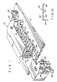
- FIG. 1 is a rear perspective view of an exemplary right-angle ejection latch header mounted upon a printed circuit board in which selected portions have been cut away for reasons of clarity;
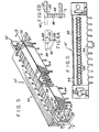
- FIG. 1A is a side view of a spring contact used with the header of FIG. 1;
- FIG. 2 is a partial rear perspective view of the ejection latch header of FIG. 1 illustrating a first tail portion connection arrangement
- FIG. 3 is similar to that shown in FIG. 2 and illustrates a second tail portion connection configuration in accordance with the present invention
- FIG. 4 similar to FIGS. 2 and 3, illustrates a third tail portion connection arrangement in accordance with the present invention
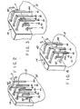
- FIG. 5 is a rear perspective view of another right-angle mounting which includes a shield member for attenuating electric field radiation from and to the tail portions;
- FIG. 6 is a rear elevational view, in cross-section, of the header of FIG. 5 taken along line 6-6 of FIG. 5;
- FIG. 6A is an enlarged detail view of the connector of FIG. 5;
- FIG. 6B is a side view, in cross section, of the view of FIG. 6A taken along line 6B-6B.
- FIG. 1 An exemplary right-angle mounted header in accordance with the present invention is illustrated in perspective view in FIG. 1 and designated generally therein by the reference character 10.
- the header 10 is mounted on the side of a printed circuit board 12 and includes a housing 14, typically fabricated from a molded thermoplastic material, and includes a base 16 and first and second spaced apart walls 18 and 20 that define a cavity or recess 22 which receives a mating connector (not shown).
- the opposite ends of the housing 14 are provided with forwardly extending projections 24, each of which includes a slot 26.
- a finger-operable latch 28 is pivotably retained in each slot 26 and is movable between a first, eject position (shown in FIG. 1) and a second position.
- the exemplary header 10 of FIG. 1 is provided with two parallel rows of contacts, typically square-sided or cylindrical pins 30, arranged in a rectangular matrix or array pattern and which are secured within the base 16 and extend forwardly into the recess 22 for engagement with the receptacles (not shown) of a mating connector.
- the pins 30 each include a tail portion, generally designated by the reference character T, that extends rearwardly of the housing 14 for effecting electrical connection with the printed circuit board 12.
- Each tail portion T includes a first segment T1 that extends linearly and rearwardly from its pin 30 and a second segment T2 that extends at an angle, typically a right angle, relative to the first segment T1 and which extends through a suitable through bore 32 formed in the printed circuit board 12.
- the header 10 is available under part number designation 66429-XXX from DuPont Electronics of New Cumberland, PA 17070.
- each spring contact 34 includes a beam portion 36, a distal end 38, a stem portion 40, and a tail portion that includes a first segment 42 that is generally in line with and extends rearwardly from the beam portion 36, and a second segment 44 that extends at a right angle relative to the first segment 42.
- the spring contacts 34 are typically stamped or pressed from a beryllium-copper alloy.
- the facing surfaces of the walls 18 and 20 of the housing are provided with respective grooves 46 for accepting the spring contacts 34.
- Each groove leads to an interior passageway (unnumbered) in the base 16 of the housing 14 from which the segment 42 extends in the rearward direction.
- the stem portion 40 includes various retention barbs or spurs (unnumbered) that engage the sides of the interior passageway to retain the spring contact 34 in place.
- the various spring contacts 34 thus define an upper series or row of spaced apart spring contacts 34 above the array of pins 30 and a complementary lower row of spaced apart spring contacts 34 below the array of pins 30.
- the grooves in which the spring contacts 34 are positioned provide sufficient clearance to allow the beam portion to be resiliently biased toward the pins 30.
- the tail portions T of the various pins 30 and the segments 42 and 44 of the spring contacts 34 extend from the rear of the housing 14 with the tail portions of the spring contacts 34 arranged between or intermediate those of the pins 30.
- the various tail portions of the pins 30 and contacts 34 are connected to the printed circuit board 12 to minimize electric field radiation from the various signal-carrying circuits, and, conversely, minimize the adverse affect of external electric fields on the signal-carrying circuits.
- the first segments T1 of the tail portions of the lower row of pins 30 extend rearwardly from the housing 14 and are bent downwardly at a right angle with respective segment T2 extending through a corresponding hole 32 in the printed circuit board 12.
- the first segments T1 of the uppermost row of pins 30 extend a selected distance rearwardly of the housing 14 and are then bent downwardly at a right angle with the respective segment T2 extending through their respective holes 32 in the printed circuit board 12.
- the segments T1 for the tail portions T of the uppermost row of pins 30 are longer than the corresponding segments T1 for the lower row of pins 30 in order to provide sufficient front-to-rear spacing between the descending segments T2 of the upper and lower rows of pins 30.
- first segments 42 of the upper row of spring contacts 34 extends rearwardly a selected distance from the housing 14 and are bent downwardly at a right angle with the second segments 44 extending into holes 32 in the printed circuit board 12.
- first segments 42 of the lower row of spring contacts 34 extends rearwardly from the housing 14 and are bent downwardly at a right angle so the second segments 44 extend into respective holes 32 in the printed circuit board 12.
- the first segments 42 for both the uppermost and lowermost rows of the spring contacts 34 extend an identical or near identical distance from the rear of the housing 14 so that the second segment 44 of the uppermost row and the second segment 44 of the lowermost row engage each other in adjacent planes and pass through the same hole 32 in the printed circuit board.
- each column of pins 30 provides tail portions T that are interdigitated with the first segments 42 and the second segments 44 of the spring contacts 34. It has been found that the interdigitated arrangement of the first segments and second segments of the spring contacts 34 as described above and as shown in FIG. 2 minimizes or at least greatly attenuates electric field radiation from the intermediate signal-carrying tail portions and, conversely, minimizes adverse effects on the signal-carrying circuits from external fields.
- FIG. 3 A first variation of the configuration of FIG. 2 is illustrated in FIG. 3, and, as shown therein, the tail portions T of the various pins 30 are arranged in a manner identical to that shown in FIG. 2 with the first segments T1 extending rearwardly from the housing 14 and with the second segments T2 extending at a right angle and downwardly to and through respective holes 32 in the printed circuit board 12.
- the first segments 42 and second segments 44 of the lower row of spring contacts 34 are configured identically to that of FIG. 2, that is, the first segments 42 extend a selected distance rearwardly from the housing 14 and then are bent at a right angle downwardly with the second segments 44 extending into respective receiving holes 32 in the printed circuit board 12.
- the configuration of FIG. 3 In contrast to the configuration of FIG.
- the first segments 42 of the upper row of spring contacts 34 extend a substantially greater distance rearwardly than the first segments 42 of the lowermost row and, additionally, the first segments T1 of the uppermost row of pins 30.
- the second segments T2 are then directed at a right angle downwardly into respective receiving holes 32 in the printed circuit board 12. Accordingly, the second segments 44 of the upper and lower row of spring contacts 34 are spaced front-to-rear from one another in a manner analogous to that of the various second segments T2 of the various tails T.
- FIG. 4 A second variation of the configuration of FIG. 2 is illustrated in FIG. 4, and, as shown therein, the tail portions T of the various pins 30 are arranged in a manner identical to that shown in FIGS. 2 and 3 with the first segments T1 extending rearwardly from the housing 14 and with the second segments T2 extending at a right angle and downwardly to and through respective holes 32 in the printed circuit board 12.
- the first segments 42 and second segments 44 of the upper row of spring contacts 34 are configured identically to that of FIG. 3, that is, the first segments 42 extend a selected distance rearwardly from the housing 14 and then are bent at a right angle downwardly with the second segments 44 extending into respective receiving holes 32 in the printed circuit board 12.
- the configuration of FIG. 4 In contrast to the configuration of FIG.
- the first segments 42 of the lower row of spring contacts 34 extend a similar distance rearwardly as the first segments 42 of the upper row of pins 30.
- the second segments T2 are then directed at a right angle downwardly into respective receiving holes 32 in the printed circuit board 12, these holes 32 being the same that accommodate the second segments 44 of the upper row of pins. Accordingly, the second segments 44 of the upper and lower row of spring contacts 34 are generally rearward of the second segments T2 of the pin contacts.
- FIGS. 2, 3, and 4 serves to position a number of grounded, conductive first and second segments 42 and 44 in an interdigitated fashion with the signal carrying tail portions P. It has been found that the presence of the first and second segments 42 and 44 serves to attenuate electric field emission from the individual signal-carrying circuits as well attenuate the effect of external fields on the signal carrying conductors in a cost-effective manner.
- FIGS. 5 and 6 A second variation of the header configuration of FIG. 1 is shown in FIGS. 5 and 6, and, as shown, the header 10′ includes a molded thermoplastic housing 50 having a mounting bracket 52 extending laterally from each end for mounting the header 10′ upon a printed circuit board (not shown in FIGS. 5-6).
- the header 10′ includes a base and side wall structure as described above in connection with FIG. 1 and includes upper and lower rows of pins (not shown) having tail portions T1 that extend rearwardly of the housing 50 and tail portions T2 that are bent downwardly at a right angle as described above in relationship to FIGS. 2, 3, and 4.
- the header 10′ additionally includes a set of upper row and lower row spring contacts (not specifically shown) each of which includes a first segment 42 and a second segment 44 that cooperate with a shield 56 that surrounds the tail portions T1 and T2.
- the shield 56 is fabricated from a stamped or pressed conductive sheet stock, and, as shown in FIG. 5, includes spaced parallel side walls 58 and 60 connected by a contiguous top 62 with a series of spaced depending lugs 64 extending from the lower edge of each side wall 58 and 60.
- the lugs 64 are designed to be received within appropriate receiving bores in the printed circuit board and soldered in place, with the lugs typically making contact with appropriate ground traces or a ground plane fabricated as part of the printed circuit board. As best shown in FIG.
- the side wall 58 is provided with a series of adjacent, vertically elongated openings 66 through which the segments T1 of the various tail portions of the upper and lower rows of pins extend.
- the top wall, at the intersection of the side wall 58, as best shown in FIG. 6A and 6B, are provided with a series of spaced semicircular cut-outs 68 that are in alignment with the first segments 42 of the upper row of spring contacts.
- the rearwardly extending first segments 42 of the various spring contacts of the upper row extend over the top of the side wall 58 at each cut-out 68 with the second segments 44 bent downwardly at a right angle to crimp and thereby secure the side wall 58 against the rear of the header housing 50.
- the lower edge of the side wall 58 is similarly crimped with the second segments 44 of the lower row of spring contacts.
- the spring contacts of the upper and lower rows are used to effectively secure the shield 56 to the rear of the housing and provide both mechanical and electrical connection with the spring contacts.
- the invention has been described above in the context of two-row headers utilizing pins mounted in a housing; as can be appreciated, the invention is equally suited to headers using more or less than two rows of contacts as well as connectors utilizing receptacles mounted in a housing.
Landscapes
- Details Of Connecting Devices For Male And Female Coupling (AREA)
- Coupling Device And Connection With Printed Circuit (AREA)
- Shielding Devices Or Components To Electric Or Magnetic Fields (AREA)
- Fire-Detection Mechanisms (AREA)
Priority Applications (1)
| Application Number | Priority Date | Filing Date | Title |
|---|---|---|---|
| AT89307404T ATE100636T1 (de) | 1988-07-20 | 1989-07-20 | Abschirmung eines buchsenleiters fuer kopfgehaeuse und verbindungsstecker. |
Applications Claiming Priority (2)
| Application Number | Priority Date | Filing Date | Title |
|---|---|---|---|
| US07/222,090 US4874319A (en) | 1988-07-20 | 1988-07-20 | Terminal lead shielding for headers and connectors |
| US222090 | 1998-12-29 |
Publications (3)
| Publication Number | Publication Date |
|---|---|
| EP0355048A2 true EP0355048A2 (de) | 1990-02-21 |
| EP0355048A3 EP0355048A3 (en) | 1990-02-28 |
| EP0355048B1 EP0355048B1 (de) | 1994-01-19 |
Family
ID=22830775
Family Applications (1)
| Application Number | Title | Priority Date | Filing Date |
|---|---|---|---|
| EP89307404A Expired - Lifetime EP0355048B1 (de) | 1988-07-20 | 1989-07-20 | Abschirmung eines Buchsenleiters für Kopfgehäuse und Verbindungsstecker |
Country Status (8)
| Country | Link |
|---|---|
| US (1) | US4874319A (de) |
| EP (1) | EP0355048B1 (de) |
| JP (1) | JPH0779031B2 (de) |
| KR (1) | KR0139000B1 (de) |
| AT (1) | ATE100636T1 (de) |
| CA (1) | CA1299687C (de) |
| DE (1) | DE68912448T2 (de) |
| HK (1) | HK1000405A1 (de) |
Cited By (1)
| Publication number | Priority date | Publication date | Assignee | Title |
|---|---|---|---|---|
| EP0455367A2 (de) * | 1990-05-04 | 1991-11-06 | The Whitaker Corporation | Rechtwinklig abgebogener impedanzangepasster Steckverbinder |
Families Citing this family (11)
| Publication number | Priority date | Publication date | Assignee | Title |
|---|---|---|---|---|
| CA2018400C (en) * | 1989-06-07 | 1993-08-24 | Tsunesuke Takano | Electrical connectors |
| US5141453A (en) * | 1990-06-08 | 1992-08-25 | E. I. Du Pont De Nemours And Company | Connectors with ground structure |
| US5151036A (en) * | 1990-06-08 | 1992-09-29 | E. I. Du Pont De Nemours And Company | Connectors with ground structure |
| AU7736691A (en) * | 1990-06-08 | 1991-12-12 | E.I. Du Pont De Nemours And Company | Connectors with ground structure |
| US5228864A (en) * | 1990-06-08 | 1993-07-20 | E. I. Du Pont De Nemours And Company | Connectors with ground structure |
| US5035634A (en) * | 1990-06-28 | 1991-07-30 | E. I. Du Pont De Nemours And Company | Connector inject and eject cam lever assembly |
| US5030115A (en) * | 1990-07-23 | 1991-07-09 | Molex Incorporated | Tired socket assembly with integral ground shield |
| JPH0521110A (ja) * | 1991-07-10 | 1993-01-29 | Amp Japan Ltd | シールド型電気コネクタ |
| JPH06163123A (ja) * | 1992-11-26 | 1994-06-10 | Nec Corp | 多極コネクタ |
| US5443394A (en) * | 1994-05-04 | 1995-08-22 | The Whitaker Corporation | Card edge connector having positive lock and extractor |
| US5635775A (en) * | 1995-04-14 | 1997-06-03 | Colburn; Richard H. | Printed circuit board mount electro-magnetic interference suppressor |
Citations (3)
| Publication number | Priority date | Publication date | Assignee | Title |
|---|---|---|---|---|
| GB2027290A (en) * | 1978-07-21 | 1980-02-13 | Siemens Ag | Electrical pin arrangements |
| EP0188876A1 (de) * | 1984-12-21 | 1986-07-30 | Molex Incorporated | Anordnung für einen abgeschirmten elektrischen Verbinder |
| US4697864A (en) * | 1986-06-19 | 1987-10-06 | Amp Incorporated | Printed circuit board receptacle for sealed connector |
Family Cites Families (14)
| Publication number | Priority date | Publication date | Assignee | Title |
|---|---|---|---|---|
| US4025141A (en) * | 1976-01-28 | 1977-05-24 | E. I. Du Pont De Nemours And Company | Electrical connector block |
| US4005921A (en) * | 1976-02-23 | 1977-02-01 | E. I. Du Pont De Nemours And Company | Transmission cable connector and termination method |
| CA1098600A (en) * | 1977-12-22 | 1981-03-31 | Donald P.G. Walter | Electrical connector shielded against interference |
| EP0090539A3 (de) * | 1982-03-31 | 1985-11-21 | AMP INCORPORATED (a New Jersey corporation) | Abgeschirmter Verbinder |
| US4687263A (en) * | 1983-03-10 | 1987-08-18 | Amp Incorporated | Shielding kit for electrical connectors terminating multiconductor 360 degree shielded cable |
| DE3327414C2 (de) * | 1983-07-29 | 1987-01-08 | Preh, Elektrofeinmechanische Werke Jakob Preh Nachf. Gmbh & Co, 8740 Bad Neustadt | Buchsenleiste |
| US4655518A (en) * | 1984-08-17 | 1987-04-07 | Teradyne, Inc. | Backplane connector |
| US4606596A (en) * | 1984-11-19 | 1986-08-19 | E. I. Du Pont De Nemours And Company | Stress relief apparatus for electrical connectors |
| US4601527A (en) * | 1985-01-18 | 1986-07-22 | E. I. Du Pont De Nemours And Company | Shielded header and cable assembly |
| US4624515A (en) * | 1985-04-17 | 1986-11-25 | Thomas & Betts Corporation | Electrical connector with grounding clip |
| US4686607A (en) * | 1986-01-08 | 1987-08-11 | Teradyne, Inc. | Daughter board/backplane assembly |
| US4737116A (en) * | 1986-04-21 | 1988-04-12 | Micro Component Technology, Inc. | Impedance matching block |
| JPH0746622B2 (ja) * | 1986-05-30 | 1995-05-17 | アンプ インコ−ポレ−テツド | 多極シ−ルドコネクタ |
| US4734042A (en) * | 1987-02-09 | 1988-03-29 | Augat Inc. | Multi row high density connector |
-
1988
- 1988-07-20 US US07/222,090 patent/US4874319A/en not_active Expired - Lifetime
-
1989
- 1989-07-19 CA CA000606119A patent/CA1299687C/en not_active Expired - Lifetime
- 1989-07-20 KR KR1019890010298A patent/KR0139000B1/ko not_active IP Right Cessation
- 1989-07-20 AT AT89307404T patent/ATE100636T1/de not_active IP Right Cessation
- 1989-07-20 EP EP89307404A patent/EP0355048B1/de not_active Expired - Lifetime
- 1989-07-20 DE DE68912448T patent/DE68912448T2/de not_active Expired - Fee Related
- 1989-07-20 JP JP1188702A patent/JPH0779031B2/ja not_active Expired - Fee Related
-
1997
- 1997-10-21 HK HK97101987A patent/HK1000405A1/xx not_active IP Right Cessation
Patent Citations (3)
| Publication number | Priority date | Publication date | Assignee | Title |
|---|---|---|---|---|
| GB2027290A (en) * | 1978-07-21 | 1980-02-13 | Siemens Ag | Electrical pin arrangements |
| EP0188876A1 (de) * | 1984-12-21 | 1986-07-30 | Molex Incorporated | Anordnung für einen abgeschirmten elektrischen Verbinder |
| US4697864A (en) * | 1986-06-19 | 1987-10-06 | Amp Incorporated | Printed circuit board receptacle for sealed connector |
Cited By (2)
| Publication number | Priority date | Publication date | Assignee | Title |
|---|---|---|---|---|
| EP0455367A2 (de) * | 1990-05-04 | 1991-11-06 | The Whitaker Corporation | Rechtwinklig abgebogener impedanzangepasster Steckverbinder |
| EP0455367A3 (en) * | 1990-05-04 | 1992-09-09 | Amp Incorporated | Right angle impedance matched electrical connector |
Also Published As
| Publication number | Publication date |
|---|---|
| US4874319A (en) | 1989-10-17 |
| JPH0779031B2 (ja) | 1995-08-23 |
| EP0355048B1 (de) | 1994-01-19 |
| KR900002495A (ko) | 1990-02-28 |
| KR0139000B1 (ko) | 1998-06-15 |
| DE68912448T2 (de) | 1994-07-14 |
| ATE100636T1 (de) | 1994-02-15 |
| HK1000405A1 (en) | 1998-03-13 |
| JPH02177278A (ja) | 1990-07-10 |
| EP0355048A3 (en) | 1990-02-28 |
| CA1299687C (en) | 1992-04-28 |
| DE68912448D1 (de) | 1994-03-03 |
Similar Documents
| Publication | Publication Date | Title |
|---|---|---|
| US5697799A (en) | Board-mountable shielded electrical connector | |
| US5531612A (en) | Multi-port modular jack assembly | |
| US5586893A (en) | IC card connector shield grounding | |
| US5055069A (en) | Connectors with ground structure | |
| KR960002136B1 (ko) | 접지 구조물을 갖고 있는 커넥터 | |
| US5688130A (en) | Electrical connector assembly for pc cards | |
| US6682368B2 (en) | Electrical connector assembly utilizing multiple ground planes | |
| US6471548B2 (en) | Shielded header | |
| US5934940A (en) | Shielded electrical connector | |
| US4913664A (en) | Miniature circular DIN connector | |
| US5876222A (en) | Electrical connector for printed circuit boards | |
| US5228864A (en) | Connectors with ground structure | |
| US5135405A (en) | Connectors with ground structure | |
| US4619487A (en) | Flat cable connector with grounding clip | |
| KR970001948B1 (ko) | 일체로 된 접지 단자 및 테일 실드 | |
| EP0263654A2 (de) | ylektrischer Stecker und Anordnung eines Steckverbinderempfängers | |
| US5415566A (en) | Shielded electrical connector assembly | |
| US5725394A (en) | Grounding system for IC cards | |
| US4874319A (en) | Terminal lead shielding for headers and connectors | |
| US20100003852A1 (en) | Electrical connector with improved grounding | |
| US6739915B1 (en) | Electrical connector with rear retention mechanism of outer shell | |
| GB2296829A (en) | Printed circuit board connector | |
| WO1998013904A1 (en) | Hybrid grounded and stacked connector assembly with audio jacks | |
| US5151036A (en) | Connectors with ground structure | |
| US5141453A (en) | Connectors with ground structure |
Legal Events
| Date | Code | Title | Description |
|---|---|---|---|
| PUAI | Public reference made under article 153(3) epc to a published international application that has entered the european phase |
Free format text: ORIGINAL CODE: 0009012 |
|
| PUAL | Search report despatched |
Free format text: ORIGINAL CODE: 0009013 |
|
| AK | Designated contracting states |
Kind code of ref document: A2 Designated state(s): AT BE CH DE ES FR GB IT LI LU NL SE |
|
| AK | Designated contracting states |
Kind code of ref document: A3 Designated state(s): AT BE CH DE ES FR GB IT LI LU NL SE |
|
| 17P | Request for examination filed |
Effective date: 19900221 |
|
| 17Q | First examination report despatched |
Effective date: 19921014 |
|
| GRAA | (expected) grant |
Free format text: ORIGINAL CODE: 0009210 |
|
| AK | Designated contracting states |
Kind code of ref document: B1 Designated state(s): AT BE CH DE ES FR GB IT LI LU NL SE |
|
| PG25 | Lapsed in a contracting state [announced via postgrant information from national office to epo] |
Ref country code: IT Free format text: LAPSE BECAUSE OF FAILURE TO SUBMIT A TRANSLATION OF THE DESCRIPTION OR TO PAY THE FEE WITHIN THE PRE;WARNING: LAPSES OF ITALIAN PATENTS WITH EFFECTIVE DATE BEFORE 2007 MAY HAVE OCCURRED AT ANY TIME BEFORE 2007. THE CORRECT EFFECTIVE DATE MAY BE DIFFERENT FROM THE ONE RECORDED.SCRIBED TIME-LIMIT Effective date: 19940119 Ref country code: LI Effective date: 19940119 Ref country code: ES Free format text: THE PATENT HAS BEEN ANNULLED BY A DECISION OF A NATIONAL AUTHORITY Effective date: 19940119 Ref country code: CH Effective date: 19940119 Ref country code: AT Effective date: 19940119 Ref country code: BE Effective date: 19940119 Ref country code: NL Effective date: 19940119 Ref country code: SE Effective date: 19940119 |
|
| REF | Corresponds to: |
Ref document number: 100636 Country of ref document: AT Date of ref document: 19940215 Kind code of ref document: T |
|
| ET | Fr: translation filed | ||
| REF | Corresponds to: |
Ref document number: 68912448 Country of ref document: DE Date of ref document: 19940303 |
|
| REG | Reference to a national code |
Ref country code: CH Ref legal event code: PL |
|
| NLV1 | Nl: lapsed or annulled due to failure to fulfill the requirements of art. 29p and 29m of the patents act | ||
| PG25 | Lapsed in a contracting state [announced via postgrant information from national office to epo] |
Ref country code: LU Free format text: LAPSE BECAUSE OF NON-PAYMENT OF DUE FEES Effective date: 19940731 |
|
| PLBE | No opposition filed within time limit |
Free format text: ORIGINAL CODE: 0009261 |
|
| STAA | Information on the status of an ep patent application or granted ep patent |
Free format text: STATUS: NO OPPOSITION FILED WITHIN TIME LIMIT |
|
| 26N | No opposition filed | ||
| REG | Reference to a national code |
Ref country code: GB Ref legal event code: 732E |
|
| REG | Reference to a national code |
Ref country code: FR Ref legal event code: TP |
|
| REG | Reference to a national code |
Ref country code: GB Ref legal event code: 732E |
|
| REG | Reference to a national code |
Ref country code: GB Ref legal event code: IF02 |
|
| PGFP | Annual fee paid to national office [announced via postgrant information from national office to epo] |
Ref country code: GB Payment date: 20020613 Year of fee payment: 14 |
|
| PGFP | Annual fee paid to national office [announced via postgrant information from national office to epo] |
Ref country code: FR Payment date: 20020702 Year of fee payment: 14 |
|
| PGFP | Annual fee paid to national office [announced via postgrant information from national office to epo] |
Ref country code: DE Payment date: 20020731 Year of fee payment: 14 |
|
| PG25 | Lapsed in a contracting state [announced via postgrant information from national office to epo] |
Ref country code: GB Free format text: LAPSE BECAUSE OF NON-PAYMENT OF DUE FEES Effective date: 20030720 |
|
| PG25 | Lapsed in a contracting state [announced via postgrant information from national office to epo] |
Ref country code: DE Free format text: LAPSE BECAUSE OF NON-PAYMENT OF DUE FEES Effective date: 20040203 |
|
| GBPC | Gb: european patent ceased through non-payment of renewal fee |
Effective date: 20030720 |
|
| PG25 | Lapsed in a contracting state [announced via postgrant information from national office to epo] |
Ref country code: FR Free format text: LAPSE BECAUSE OF NON-PAYMENT OF DUE FEES Effective date: 20040331 |
|
| REG | Reference to a national code |
Ref country code: FR Ref legal event code: ST |