EP0353725A2 - Raster deflection signal generation apparatus - Google Patents
Raster deflection signal generation apparatus Download PDFInfo
- Publication number
- EP0353725A2 EP0353725A2 EP89114229A EP89114229A EP0353725A2 EP 0353725 A2 EP0353725 A2 EP 0353725A2 EP 89114229 A EP89114229 A EP 89114229A EP 89114229 A EP89114229 A EP 89114229A EP 0353725 A2 EP0353725 A2 EP 0353725A2
- Authority
- EP
- European Patent Office
- Prior art keywords
- signal
- sweep
- signals
- raster
- deflection
- Prior art date
- Legal status (The legal status is an assumption and is not a legal conclusion. Google has not performed a legal analysis and makes no representation as to the accuracy of the status listed.)
- Granted
Links
Images


Classifications
-
- H—ELECTRICITY
- H04—ELECTRIC COMMUNICATION TECHNIQUE
- H04N—PICTORIAL COMMUNICATION, e.g. TELEVISION
- H04N3/00—Scanning details of television systems; Combination thereof with generation of supply voltages
- H04N3/10—Scanning details of television systems; Combination thereof with generation of supply voltages by means not exclusively optical-mechanical
- H04N3/16—Scanning details of television systems; Combination thereof with generation of supply voltages by means not exclusively optical-mechanical by deflecting electron beam in cathode-ray tube, e.g. scanning corrections
- H04N3/22—Circuits for controlling dimensions, shape or centering of picture on screen
- H04N3/227—Centering
Landscapes
- Engineering & Computer Science (AREA)
- Multimedia (AREA)
- Signal Processing (AREA)
- Controls And Circuits For Display Device (AREA)
- Details Of Television Scanning (AREA)
- Digital Computer Display Output (AREA)
Abstract
Description
- The invention relates to a raster deflection signal generation apparatus according to the preamble of
claim 1. - Cathode ray tube displays for conveying television picture information are ubiquitous in present day technologies. For example, complex avionics systems utilize cathode ray tube displays to replace many formally mechanical flight instruments as well as to additionally provide other complex display information to the operator. Generally, the data is provided in the form of a television raster scan or in the form of calligraphic stroke written symbology. Such avionics systems require the presentation of the television raster images with accurately positioned stroke written symbols overlayed thereon. Modern aircraft instrumentation of this type is frequently referred to as a "glass cockpit". Such avionics systems often utilize a plurality of television sensor inputs with diverse video formats to be displayed on a plurality of display devices. Each display processing channel must synchronize its operation to the diverse timing information present in the television input signals. Specifically, horizontal and vertical synchronizing pulses permit a picture image to be properly placed upon a CRT screen. Each of the television signal inputs can vary in its timing characteristics adversely affecting te positional accuracy of the presentation. The positional accuracy problem is further exacerbated in modern complex avionics systems because of the large number of distinct input and output signal characteristics.
- The signals required to drive the CRT displays comprise primarily a video or intensity electrical signal, the instantaneous amplitude of which translates into a proportional intensity on the CRT screen and a pair of periodic sawtooth deflection control signals. The deflection signals are denoted as horizontal or X and vertical or Y deflections and comprise electrical signals with amplitudes resulting in proportional deflections from the CRT screen center in the respective horizontal and vertical directions.
- In order to provide a set of signals of the correct characteristics, resettable integrators are utilized to provide the linear deflection sweeps. Conventional deflection generators are, however, subject to inaccuracies in the generation circuitry. These inaccuracies result from the timing variations discussed above as well as because of drift in component characteristics due to environmental conditions such as variations in temperature.
- Several methods are utilized in the prior art to overcome these inaccuracies. Firstly, overscanning may be utilized wherein the picture size is expanded until the image size significantly exceeds the screen size. Although overscanning eliminates objectionable blank areas at the CRT screen edges and permits the deflection generation characteristics to drift without noticeably disturbing the image, overscanning is unacceptable for avionics applications, particularly in military systems, since a loss of picture information and positional accuracy occurs in the offscreen area.
- A second prior art solution involves precisely adjusting the characteristics of each deflection generator. This solution requires the use of high precision and temperature stable electrical components to generate a precisely placed image. Each of the X and Y deflection signal generators is precisely adjusted by the use of signal offset and gain adjustment trimming mechanisms. This approach is cumbersome for multiple sensor applications since a new adjustment value must be provided for each sensor input. The solution becomes inordinately complex when a large number of systematic timing variations must be accommodated. In the prior art, individual sensor variations are accommodated by attempting to design and match an analog deflection network to each of a number of input characteristics by utilizing analog switching means.
- It is, therefore, the object of the present invention to devise a raster deflection signal generation apparatus which operates extremely accurate without requiring high precision components. This objects is achieved according to the characterizing features of
claim 1. Further advantageous embodiments of the inventive apparatus may be taken from the dependent claims. - The present invention utilizes a programmable timing generator to convert the timing information in the television sensor input signals into sweep signals corrected for timing variations by digital data stored in the programmable timing generator. The sweep signals are applied to closed loop adaptive deflection signal generators that maintain the sweeps screen centered irrespective of timing variations and drift of characteristics.
-
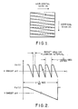
- Figure 1 is a graphical representation of a television raster scan. A television image is generated by the left-to-right, top-to-bottom scan of an intensity modulated electron beam.
- Figure 2 is a graph illustrating the display deflection waveforms. The horizontal (X) and vertical (Y) deflection signals control the position of the electron beam.
- Figure 3 is a schematic block diagram of a display channel raster deflection generator implemented in accordance with the present invention.
- Figure 4 is a schematic block diagram illustrating details of the programmable timing generator of Figure 3.
- Figure 5 is a schematic block diagram illustrating details of each of the X-sweep generator and the Y-sweep generator of Figure 3.
- Figure 6 is a graph illustrating waveforms useful in explaining the operation of the invention.
- Referring to Figure 1, a conventional television raster scan is graphically illustrated. In the present embodiment, the raster scan begins just offscreen in the upper lefthand corner and ends just offscreen in the lower righthand corner.
Conventionally, the television frames may be interlaced by alternately displaying the odd and even Y lines. - Referring to Figure 2, the deflection waveforms illustrated provide an accurately positioned television image. It is noted that each of the sweep waveforms is linear and d.c. balanced. For each X sweep and Y sweep, the beam crosses screen center when the deflection waveform is zero volts. Thus, for a correctly positioned image, the active portion of each sweep is positive and negative for equal periods of time if the reset or blanking interval is eliminated. If the center of the image should drift horizontally from screen center, the X sweep waveforms would no longer be d.c. balanced. Similarly, if the center of the image should drift vertically from screen center, the Y sweep waveforms would no longer be d.c. balanced. This property is utilized in a manner to be later described in maintaining the center of the TV image at screen center. The size and position of the television image depend on the absolute accuracy of the X and Y deflection waveforms.
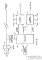
- Referring to Figure 3, a schematic block diagram of the display raster deflection generator of the present invention is illustrated. A plurality of composite video (television) signals is received by an N-to-1
multiplexer 10. The composite video signals are provided from the sensor video sources of the sytem. A system central computer (not shown) selects one of the video sources by a select signal on aline 11 and provides the selected video via avideo amplifier 12 to the display device on which the television image is to be generated. The horizontal and vertical synchronization signals are separated in async separator 13 and the resulting composite sync signals are applied to aprogrammable timing generator 14. In a manner to be described, theprogrammable timing generator 14 is initialized by the central computer via an address anddata bus 15 to store the parameters required to tailor the X and Y deflection signals in accordance with the selected video source and the particular display device to be utilized. Theprogrammable timing generator 14 provides digital X and Y sweep signals to anX-sweep generator 16 and a Y-sweep generator 17, respectively. In response to the digital sweep signals, thesweep generators - The raster deflection generator of Figure 3 generates the horizontal and vertical deflection waveforms to precisely place the sensor video information on the CRT display device. In a manner to be described, individual sensor variations are accommodated by the
programmable timing generator 14 which tailors the digital X and Y sweep control signals applied to theanalog sweep generators analog generators X-sweep generator 16 receives a VBIAS signal, a VSET signal, and a VREF signal to generate the X deflection sweep signal illustrated in Figure 2. Similarly, the Y-sweep generator 17 receives a VBIAS signal, a VSET signal and a VREF signal to generate the Y deflection sweep signal illustrated in Figure 2. Bothsweep generators sweep generators - Referring to Figure 4, details of the
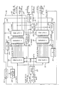
programmable timing generator 14 of Figure 3 are illustrated. Theprogrammable timing generator 14 includes X data registers 20 and Y data registers 21 for storing control values corresponding to the video source selected by the central computer. When the central computer selects a new video source, corresponding timing control values are uploaded into the digital data files 20 and 21. The address/data bus 15 from the central computer is coupled to aninput control section 22 that receives a load address signal from the computer. The load address signal controls entering the appropriate data file addresses into theinput control section 22 for routing the data to the appropriate data files. A load data signal from the central computer applied to the data files 20 and 21 controls entering the timing control values from thedata bus 15 into the appropriate X and Y data file registers specified by the addresses. The data words are ten bits wide and a total of ten registers each in X and Y is sufficient to specify all of the necessary programmable timing generator output characteristics. Amaster clock 23 drives a horizontal (X) ten bit counter 24, the ten bit output of which is applied to anX comparator 25. Thecomparator 25 compares the output of theX counter 24 with the ten bit output of each of the X data registers 20 and issues a signal to an X output register 26 when equality occurs. When the states of theX counter 24 agree with the timing values stored in the data files 20, an output of the X output register 26 changes to provide the horizontal (X) sweep control signal of the present invention in a manner to be explained. Theprogrammable timing generator 14 also provides the various synchronizing and blanking pulses required by the display. TheX output register 26 provides the horizontal sweep control signal to theX-sweep generator 16 of Figure 3 on aline 27. The X output register 26 also provides a horizontal synchronizing pulse on aline 28. - The composite sync signal from the
sync separator 13 of Figure 3 is applied to async detector 29 that extracts the horizontal syn signal from the selected video input and provides this signal on aline 30. Thesync detector 29 is responsive to the two most significant bits from theX counter 24 to ensure that only the desired horizontal synchronizing information is processed. The two MSB from theX counter 24 are utilized, in a conventional manner, to gate through such desired horizontal synchronising information while blocking extraneous timing pulses present in certain video formats during the vertical sync interval. These pulses are blocked to assure proper operation of the servo loop in which the signal on theline 30 is utilized. The two bits of address provide qualification to approximately one-quarter horizontal line time. - The signal on the
line 30 may be referred to as a lock-on sync (LOS) signal. The detected sync information on theline 30 and the horizontal synchronizing output on theline 28 from the X output register 26 are applied to aphase detector 31, the output of which provides an input to themaster clock 23. Themaster clock 23 is a voltage controlled oscillator having a frequency that is adjusted by thephase detector 31 to cause the two synchronizing signals on thelines components 23, 28-31 comprise a phase locked loop that servoes the output signals of theprogrammable timing generator 14 to the input video signal. Thecomparator 25 also provides an output to the clear input of theX counter 24 so as to specify the maximum value of the counter range. - The
programmable timing generator 14 includes a vertical (Y) counter 32 coupled to count the horizontal sync pulses on theline 28. TheY counter 32 is ten bits wide and provides its output to aY comparator 33. TheY comparator 33 also receives the outputs from the Y data registers 21 in a manner similar to that described above with respect to theX comparator 25. A Y output register 34 is coupled to receive the outputs from theY comparator 33 and generates the vertical signals of theprogrammable timing generator 14. The signals from the Y output register 34 include the vertical sweep control signal applied to the Y-sweep generator 17 of Figure 3 as well as a vertical sync and vertical blanking pulse. The Y output register 34 also provides a phase locked loop (PLL) gate for disabling thephase detector 31 during vertical flyback to prevent anamolous operation in a manner similar to the sample and holdcircuit 61 to be discussed with respect to Figure 5. TheY comparator 33 also provides a signal to clear theY counter 32 so as to specify the maximum value of the counter range. - The
programmable timing generator 14 includes an odd/even detectcircuit 35 to detect the odd and even raster lines for use in a system employing alternate odd/even framing. The odd/even detectcircuit 35 is responsive to the vertical synchronizing pulse stripped from the composite sync by thesync detector 29 and the horizontal blanking pulse from the X output register 26 for detecting the odd and even raster lines. The ten bit ouput of theY counter 32 and the output of the odd/evendetector 35 are applied to aY multiplier 36 for providing all the even Y addresses and then all the odd Y addresses. - The eight least significant bits from the
X counter 25 and the ten Y address bits from theY multiplexer 36 are applied to anaddress register 37. Theaddress register 37 provides complete sets of horizontal and vertical addresses useable for accessing RAM image data memories. The output of themaster clock 23 is applied to theX output register 26, theY output register 34, the odd/evendetector circuit 35 and theaddress register 37 for system timing purposes. - Thus, it is appreciated that the
programmable timing generator 14 is architectured to utilize the repetitive behavior of television video signals. Each horizontal and vertical interval is decomposed into a number of critical events, e.g., start sync/stop sync. The vertical and horizontal structures each contains the ten bit counter described which is incremented at the appropriate rate. As each of thecounters - The resolution of the
programmable timing generator 14 is determined by the speed at which the logic elements of which it is constructed can function. Typically, a horizontal line time is divided into about 600 events by the highfrequency master clock 23. The resolution may therefore be as fine as one part in 600 in the horizontal aspect. Vertical resolution is on the order of a half-line time and thus is typically one part in 500 to 1,000. - Referring now to Figure 5, details of the
X sweep generator 16 and theY sweep generator 17 of Figure 3 are illustrated. Since theX sweep generator 16 is substantially identical to theY sweep generator 17, except for parameter values, the details of only one such sweep generator are provided. The periodic control waveform (horizontal (X) or vertical (Y) sweep) from theprogrammable timing generator 14 is applied to the analog sweep generator of Figure 5 at a terminal 50. The sweep control signal at the terminal 50 is applied to areset switch 51 connected across anoperational amplifier integrator 52. With theswitch 51 closed, the output VOUT on aline 53 holds at a fixed value equal to VSET. In the switch-closed position, the output voltage on theline 53 is such that the CRT beam resides off the left and top screen edges. With thereset switch 51 open, the integrator output on theline 53 slews at a steady time rate-of-change to generate a linear sweep waveform. Thus, when thereset switch 51 is opened, the integrator output on theline 53 begins sweeping linearly toward the opposite voltage polarity. - The integrator output on the
line 53 is applied to avoltage comparator 54 that senses the time at which the integrator output crosses a predetermined voltage level. Preferably, the voltage level is selected as zero volts corresponding to the CRT screen center. Thus, a threshold signal VCENTER is applied to thecomparator 54, and in the preferred embodiment of the invention, VCENTER is zero volts. Thevoltage comparator 54 functions such that when the voltage on theline 53 is greater than VCENTER, thecomparator 54 outputs 2VREF. When the voltage on theline 53 is less than VCENTER, thecomparator 54 outputs zero volts. - The output of the
comparator 54 is applied through a synchronizingswitch 55 and a line 56 to the inverting input of anerror integrator 58. The synchronizingswitch 55 is operated through aninverter 59 by the sweep control waveform applied to the terminal 50. A reference voltage VREF is applied to the non-inverting input of theerror integrator 58 and through a synchronizingswitch 60 to the line 56. The synchronizingswitch 60 is also operated by the sweep control waveform applied to the terminal 50. Operation is effected such that when thereset switch 51 is opened, the synchronizingswitch 60 is also opened and the synchronizingswitch 55 is closed. Conversely, when thereset switch 51 is closed, the synchronizingswitch 60 is also closed and the synchronizingswitch 55 is opened. - The output of the
error integrator 58 is applied to a sample and holdcircuit 61 which is also strobed by the sweep control waveform applied at the terminal 50. Alternatively, the sample and holdcircuit 61 may be strobed by the HSYNC signal on the line 28 (Figure 4) or an equivalent signal. The output of the sample and holdcircuit 61 is applied through aresistor 48 to the inverting input of theintegrator 52 which also receives a bias signal VBIAS through aresistor 49. A VSET signal is applied to the non-inverting input of theintegrator 52. The junction between theresistors integrator 52. - In a manner to be further detailed, the sweep control waveform at the terminal 50 periodically opens and closes the
reset switch 51 and the synchronising switches 55 and 60 such that a sequence of linear raster sweeps are generated by theintegrator 52. As previously discussed with respect to Figure 2, if the sweep is symmetrical with respect to zero volts at screen center, thecomparator 54 will provide a square wave with a 50% duty cycle and an amplitude that switches between 2VREF and zero. During the generation of a sweep, theswitch 55 is closed and theswitch 60 is opened. For a properly centered sweep, the input to the inverting input of theerror integrator 58 will be 2VREF for half of the sweep time and zero for the other half of the sweep time. Since VREF is applied to the non-inverting input of theerror integrator 58 and the 50% duty cycle square wave applied to the inverting input thereof will integrate to a level of VREF during the sweep time, at the end of the sweep the error output of theerror integrator 58 for a properly centered sweep is zero. It is appreciated that the actions described with respect to the square wave duty cycle are predicated on eliminating the reset or blanking interval shown in Figure 2. In the operation of the present invention, this occurs because of the functioning of the synchronizing switches 55 and 60 as described. - The sample and hold
circuit 61 is strobed when thereset switch 51 is closed thus providing the error sample when the sweep is not active. If the sweep should drift from screen center, theerror integrator 58 will generate a positive or negative error signal which when applied to theintegrator 52 via the sample and holdcircuit 61 changes theintegrator 52 sweep rate so as to recenter the television picture. Thus, the TV image is servoed to screen center. By appropriate generation of the sweep control waveform at the terminal 50 and appropriate selection of VSET, the raster sweep waveform will be properly scaled to precisely control the beam from one edge of the screen to the other. - During sweep flyback, the
reset switch 51 is closed, the synchronizingswitch 55 is opened and the synchronizingswitch 60 is closed. During this interval, VREF is applied to the inverting input of theerror integrator 58 through theswitch 60 as well as to the non-inverting input thereof to hold the input of theintegrator 58 at zero during the flyback time. Thus, the output of theerror integrator 58 is maintained constant during the retrace interval. This operation of the synchronizing switches 55 and 60 effectively eliminates the retraces interval from the error determination process. Thus, the duty cycle interval of the square wave from thecomparator 54 is independent of the period chosen for blanking and/or retrace. - It is appreciated that the output of the
error integrator 58 may be sampled at the end of the sweep just before the retrace/sync but may also be sampled during the retrace or sync interval. The differential input of theerror integrator 58 is forced to zero during the retrace interval to prevent integrating the retrace and thus introducing anamolous signals as well as to hold the output of theerror integrator 58 constant during the sample interval. The purpose of sampling the output of theerror integrator 58 during the retrace and holding the value in the sample and holdcircuit 61 during the sweep period is to provide theramp generating integrator 52 with a constant input so that the sweep will be linear. - Thus, it is appreciated that the time variations caused by device and component tolerance variations form a duty cycle value which is filtered (integrated) and fed back to the
sweep generator 52 to form automatically the repeatable and accurately centered and scaled deflection waveforms. Thecomparator 54 may be considered as a phase detector since the rate at which theintegrator 52 sweeps affects the time to zero crossings of the repetitive waveforms. This duty cycle information is filtered by theerror integrator 58 and fed back to theintegrator 52 where the feedback term alters the integrator rate. During the closed or reset position of theswitch 51, the output of thecomparator 54 is not fed back to theerror integrator 58 making the feedback independent of the reset or flyback time period. The filtering and feedback mechanism of Figure 5 permits the loop to correct itself about screen center without introducing sweep linearity errors. The sample and holdmechanism 61 updates the corrected feedback voltage to theintegrator 52 when the sweep is not active. This mechanism may utilize the same signal employed to control theintegrator 52 for maximum economy of components. - Referring to Figure 6, a single horizontal sweep generation time of a sensor video input is illustrated. It is appreciated that similar waveforms are applicable to the vertical dimension. Waveform (A) illustrates that each sensor video input may have unique and different timing characteristics. The time t at which the
horizontal sync pulse 70 occurs relative to the active video interval may vary from sensor to sensor. Additionally, the time t active may also vary from sensor to sensor. - Accordingly, by the phase locked loop techniques described above, the high
frequency master clock 23 is synchronized to the sensor where the sweep values are programmable to permit fine time resolution. The programmable timing generator 14 (Figure 4) generates the sweep control waveform (B) which is tailored to the individual sensor characteristics. The X sweep illustrated in waveform (B) exemplifies the horizontal sweep waveform provided online 27 of the programmable timing generator 14 (Figure 4). The rising edge of the X sweep closes thereset switch 51 and thesynchronization switch 60 and opens thesynchronization switch 55. The rising edge of the X sweep also strobes the sample and holdcircuit 61 to acquire an error sample from theerror amplifier 58. The falling edge of the X sweep waveform opens thereset switch 51 and thesynchronization switch 60 and closes thesynchronization switch 55. Waveform (C) illustrates the HSYNC pulse generated by theprogrammable timing generator 14 to synchronize the X sweep waveform (B) with the sensorhorizontal sync pulse 70. Waveform (C) may also be utilized to strobe the sample and holdcircuit 61 as an alternative to using the rising edge of the X sweep for this purpose. As illustrated in waveform (D), the programmable control causes a sweep voltage of the correct amplitude to be generated. The waveform is automatically screen centered as discussed above. The X sweep waveform (B) as well as the Y sweep waveform are tailored by the data stored in the X and Y data registers 20 and 21 of theprogrammable timing generator 14 such that the linear ramp portion of waveform (D) varies between the positive full screen voltage +VFS and the negative full screen voltage -VFS in coincidence with the occurrence of the video t active region of waveform (A). - It is therefore appreciated that the comparator 54 (Figure 5) evaluates the time at which the deflection voltage equals zero. Discounting the X-sweep reset or blanking interval, a correctly scaled sweep exhibits that condition at a 50% time duty cycle. The output of the
comparator 54 drives theerror integrator 58 to provide an average duty cycle control voltage utilized to correct the sweep. When the sweep is centered, the ends thereof have the correct scale factor. - The apparatus of the present invention receives a multiplicity of sensor television inputs and generates the horizontal and vertical deflection waveforms in synchronism with a selected input so as to precisely place the sensor video information on a CRT display device. The present invention corrects the signal variations resulting from the multiplicity of input characteristics by utilizing the techniques described above. Firstly, the described electronic feedback automatically causes the sweep waveforms to be screen centered on the CRT display. Secondly, the drive signals controlling the generation of the deflection signals are programmable so as to permit the feedback mechanism to accommodate the systematic variations. The use of the
programmable timing generator 14 permits the compensation to be extended to adjust for a large number of input characteristics. - The control outputs of the
programmable timing generator 14, including the horizontal and vertical sweep control signals, are programmable at arbitrary start and stop times. Prior art approaches to control signal generation rely on large quantities of non-volatile memory whereas the present invention utilizes data register storage of the critical on and off times of the repetitive signals. The present invention may utilize non-volatile memory external to the device to store the operating parameters. Because of the economy of modern PROM devices, sufficient memory space may be provided outside of theprogrammable timing generator 14 to permit a multiplicity of operating modes. The extension of this concept thus characterizes each of the system sensor video inputs and adjusts the performance of the analog sweep generators accordingly. It is appreciated that many of the systematic error effects such as comparator delay and any CRT display deflection delay are accommodated by pre-emphasizing or leading the control signals from theprogrammable timing generator 14. - It is appreciated from the foregoing that the present invention provides a high precision sawtooth deflection waveform generator for CRT displays that utilizes closed loop feedback to ensure accurate voltage level and symmetry characteristics that are independent of environmental or component variations. The invention automatically corrects the output waveforms both for variations of the components utilized to construct the invention as well as for external timing variations. The invention eliminates the requirements for critical construction or adjustments to achieve accurate amplitude and timing control. The invention further eliminates almost all precise components and the effects of component aging and drift. The invention is readily programmable without hardware adjustments.
- The performance resulting from utilizing the present invention permits the accurate presentation of a variety of television formats while retaining simplicity of physical components and immunity from environmentally related variations such as temperature effects.
Claims (10)
programmable timing generator means (14) for providing first and second sweep control signals in accordance with predetermined timing characteristics of said channel, first and second raster sweep generation means (16, 17; 52) responsive to said first and second sweep control signals, respectively, for generating respective first and second raster deflection signals in accordance therewith, and
first and second servo means (54, 58) responsive to said first and second raster deflection signals, respectively, for maintaining said first and second raster deflection signals positioned with respect to a predetermined reference so that said video image remains centered on said CRT screen.
first and second storage means (20, 21) for storing respective first and second sets of digital words for generating said first and second sweep control signals, respectively,
clock means (23) for providing a clock signal,
first and second digital counter means (24, 32), said first digital counter means being coupled to count said clock signal,
first comparator means (25) coupled to said first counter means (24) and to said first storage means (20) for comparing the output of said first counter means with said digital words stored in said first storage means for providing signals in accordance with equality therebetween, said equality signals being utilized to provide said first sweep control signal and a further sync signal,
said second digital counter means (32) being coupled to count said further sync signal, and
second comparator means (33) coupled to said second digital counter means (32) and to said second storage means (21) for comparing the output of said second digital counter means with said digital words stored in said second storage means for providing signals in accordance with equality therebetween, said equality signals being utilized to provide said second sweep control signal.
comparator means (54) responsive to said first raster deflection signal for providing a duty cycle signal in accordance with said first raster deflection signal exceeding and not exceeding a predetermined threshold,
means (58) responsive to said duty cycle signal for providing an error signal in accordance with said first raster deflection signal deviating from said predetermined reference, and
means (61) for coupling said error signal to said first raster sweep generation means (52) for controlling said first raster sweep generation means to maintain said first raster deflection signal positioned with respect to said predetermined reference.
integrator means (52), and
a reset switch (51) coupled across said integrator means (52) and responsive to said first sweep control signal (50) for enabling and resetting said integrator means in accordance with said first sweep control signal,
wherein said integrator means (52) is coupled to receive the output of said sample and hold means (61) for altering the sweep rate thereof in accordance with said error signal sample stored in said sample and hold means with said sample and hold means being responsive to said first sweep control signal (50) for taking said sample in accordance therewith.
Applications Claiming Priority (2)
| Application Number | Priority Date | Filing Date | Title |
|---|---|---|---|
| US228615 | 1988-08-04 | ||
| US07/228,615 US4874992A (en) | 1988-08-04 | 1988-08-04 | Closed loop adaptive raster deflection signal generator |
Publications (3)
| Publication Number | Publication Date |
|---|---|
| EP0353725A2 true EP0353725A2 (en) | 1990-02-07 |
| EP0353725A3 EP0353725A3 (en) | 1990-05-16 |
| EP0353725B1 EP0353725B1 (en) | 1993-11-10 |
Family
ID=22857920
Family Applications (1)
| Application Number | Title | Priority Date | Filing Date |
|---|---|---|---|
| EP89114229A Expired - Lifetime EP0353725B1 (en) | 1988-08-04 | 1989-08-02 | Raster deflection signal generation apparatus |
Country Status (5)
| Country | Link |
|---|---|
| US (1) | US4874992A (en) |
| EP (1) | EP0353725B1 (en) |
| JP (1) | JP2887759B2 (en) |
| CA (1) | CA1307593C (en) |
| DE (1) | DE68910603T2 (en) |
Cited By (1)
| Publication number | Priority date | Publication date | Assignee | Title |
|---|---|---|---|---|
| EP0449130A2 (en) * | 1990-03-26 | 1991-10-02 | Thomson Consumer Electronics, Inc. | Adjustable video/raster phasing for horizontal deflection system |
Families Citing this family (8)
| Publication number | Priority date | Publication date | Assignee | Title |
|---|---|---|---|---|
| US5369341A (en) * | 1992-12-11 | 1994-11-29 | Thomson Consumer Electronics, Inc. | Vertical retrace with zoom and centered fast retrace |
| KR0144505B1 (en) * | 1995-09-18 | 1998-08-17 | 구자홍 | A screen automatic control system and method of image idsplay equipment |
| US6260104B1 (en) * | 1998-06-30 | 2001-07-10 | Micron Technology, Inc. | Multiplexing of trim outputs on a trim bus to reduce die size |
| FR2820589B1 (en) * | 2001-02-07 | 2003-04-25 | St Microelectronics Sa | DEVICE FOR CONTROLLING A VERTICAL DEVIATION CIRCUIT OF A SPOT SCANNING A SCREEN |
| US6996286B2 (en) * | 2001-10-30 | 2006-02-07 | Analogic Corporation | Sweeping spatial filter system and method |
| US6998798B1 (en) * | 2004-08-10 | 2006-02-14 | National Semiconductor Corporation | Digitally controlled vertical S linearity correction with constant amplitude without using an AGC |
| US7697011B2 (en) * | 2004-12-10 | 2010-04-13 | Honeywell International Inc. | Automatic display video positioning and scaling system |
| CN104299543B (en) * | 2013-11-29 | 2017-01-25 | 中国航空工业集团公司洛阳电光设备研究所 | CRT display driver and CRT display driving method for head-up displays |
Citations (2)
| Publication number | Priority date | Publication date | Assignee | Title |
|---|---|---|---|---|
| US4149264A (en) * | 1976-06-02 | 1979-04-10 | Hitachi, Ltd. | CRT display apparatus of raster scanning type |
| EP0130247A1 (en) * | 1983-06-30 | 1985-01-09 | International Business Machines Corporation | Programmable timing circuit for cathode ray tube |
Family Cites Families (4)
| Publication number | Priority date | Publication date | Assignee | Title |
|---|---|---|---|---|
| FR2441964A1 (en) * | 1978-11-14 | 1980-06-13 | Thomson Csf | CIRCUIT FOR GENERATING SAW TEETH, PARTICULARLY FOR LINE-BY-LINE CATHODE-SCAN, AND DEVICE COMPRISING SUCH A CIRCUIT |
| US4729024A (en) * | 1985-03-19 | 1988-03-01 | Canon Kabushiki Kaisha | Synchronizing pulse signal generation device |
| US4709268A (en) * | 1985-07-29 | 1987-11-24 | Fuji Photo Film Co., Ltd. | Automatic frequency pulling circuit |
| US4779132A (en) * | 1987-07-08 | 1988-10-18 | Zenith Electronics Corporation | Video monitor using encoded sync signals |
-
1988
- 1988-08-04 US US07/228,615 patent/US4874992A/en not_active Expired - Lifetime
-
1989
- 1989-08-02 DE DE89114229T patent/DE68910603T2/en not_active Expired - Fee Related
- 1989-08-02 EP EP89114229A patent/EP0353725B1/en not_active Expired - Lifetime
- 1989-08-03 CA CA000607423A patent/CA1307593C/en not_active Expired - Fee Related
- 1989-08-04 JP JP1201501A patent/JP2887759B2/en not_active Expired - Fee Related
Patent Citations (2)
| Publication number | Priority date | Publication date | Assignee | Title |
|---|---|---|---|---|
| US4149264A (en) * | 1976-06-02 | 1979-04-10 | Hitachi, Ltd. | CRT display apparatus of raster scanning type |
| EP0130247A1 (en) * | 1983-06-30 | 1985-01-09 | International Business Machines Corporation | Programmable timing circuit for cathode ray tube |
Cited By (4)
| Publication number | Priority date | Publication date | Assignee | Title |
|---|---|---|---|---|
| EP0449130A2 (en) * | 1990-03-26 | 1991-10-02 | Thomson Consumer Electronics, Inc. | Adjustable video/raster phasing for horizontal deflection system |
| EP0449130A3 (en) * | 1990-03-26 | 1993-05-26 | Thomson Consumer Electronics, Inc. | Adjustable video/raster phasing for horizontal deflection system |
| TR27621A (en) * | 1990-03-26 | 1995-06-13 | Thomson Consumer Electronics | Adjustable video / raster phasing for horizontal deflection system. |
| US5619276A (en) * | 1990-03-26 | 1997-04-08 | Thomson Consumer Electronics, Inc. | Adjustable video/raster phasing for horizontal deflection system |
Also Published As
| Publication number | Publication date |
|---|---|
| CA1307593C (en) | 1992-09-15 |
| DE68910603T2 (en) | 1994-03-24 |
| EP0353725B1 (en) | 1993-11-10 |
| JP2887759B2 (en) | 1999-04-26 |
| US4874992A (en) | 1989-10-17 |
| EP0353725A3 (en) | 1990-05-16 |
| DE68910603D1 (en) | 1993-12-16 |
| JPH02146584A (en) | 1990-06-05 |
Similar Documents
| Publication | Publication Date | Title |
|---|---|---|
| EP0189195A2 (en) | Apparatus for correcting time base error of video signal | |
| EP0353725B1 (en) | Raster deflection signal generation apparatus | |
| US3893036A (en) | Precision function generator | |
| US6404459B1 (en) | Display with scan converter for converting scanning frequency of input video signal | |
| US4905085A (en) | Synchronous sampling system | |
| EP0473771B1 (en) | Display locked timing signals for video processing | |
| EP0647933A1 (en) | Dot clock generator for liquid crystal display device | |
| US5250879A (en) | Deflection circuit having a controllable sawtooth generator | |
| US4695805A (en) | Apparatus for generating signals synchronized to an unstable external signal | |
| US3382436A (en) | Panoramic solid-lined and dotted graphic display systems | |
| US4833371A (en) | Picture display device with symmetrical deflection | |
| EP0024476A1 (en) | Improvements relating to line scan circuits for cathode ray tube displays | |
| KR960013315B1 (en) | Video display apparatus | |
| US3713000A (en) | Sweep generator with automatic centering | |
| CA2000011C (en) | Self-adapting vertical scan circuit for raster-scanned cathode ray tube displays | |
| US6034736A (en) | Digital horizontal flyback control circuit | |
| US4954784A (en) | Phase adjustment circuit | |
| US4754330A (en) | Display deflection control loop | |
| US5544202A (en) | Synchronization apparatus | |
| US4837464A (en) | Phase regulation circuit, particularly for horizontal phase regulation in data displays | |
| US5627596A (en) | Video synchronization circuit comprising a PLL with a circuit to set the frequency of the output signal when the feedback signal is not present | |
| US5047855A (en) | Picture pick-up or display device for successive scanning in opposing direction includes a circuit for assuring vertical symmetry of the video signal being displayed | |
| JP2584063B2 (en) | Pseudo sync signal generator | |
| JP2588584B2 (en) | Digital convergence correction device | |
| JPH05161029A (en) | Horizontal phase adjustment circuit |
Legal Events
| Date | Code | Title | Description |
|---|---|---|---|
| PUAI | Public reference made under article 153(3) epc to a published international application that has entered the european phase |
Free format text: ORIGINAL CODE: 0009012 |
|
| AK | Designated contracting states |
Kind code of ref document: A2 Designated state(s): DE FR GB IT |
|
| PUAL | Search report despatched |
Free format text: ORIGINAL CODE: 0009013 |
|
| AK | Designated contracting states |
Kind code of ref document: A3 Designated state(s): DE FR GB IT |
|
| 17P | Request for examination filed |
Effective date: 19901109 |
|
| 17Q | First examination report despatched |
Effective date: 19920929 |
|
| GRAA | (expected) grant |
Free format text: ORIGINAL CODE: 0009210 |
|
| AK | Designated contracting states |
Kind code of ref document: B1 Designated state(s): DE FR GB IT |
|
| REF | Corresponds to: |
Ref document number: 68910603 Country of ref document: DE Date of ref document: 19931216 |
|
| ET | Fr: translation filed | ||
| ITF | It: translation for a ep patent filed |
Owner name: BARZANO' E ZANARDO ROMA S.P.A. |
|
| PLBE | No opposition filed within time limit |
Free format text: ORIGINAL CODE: 0009261 |
|
| STAA | Information on the status of an ep patent application or granted ep patent |
Free format text: STATUS: NO OPPOSITION FILED WITHIN TIME LIMIT |
|
| 26N | No opposition filed | ||
| PGFP | Annual fee paid to national office [announced via postgrant information from national office to epo] |
Ref country code: FR Payment date: 19950613 Year of fee payment: 7 |
|
| PGFP | Annual fee paid to national office [announced via postgrant information from national office to epo] |
Ref country code: GB Payment date: 19950614 Year of fee payment: 7 |
|
| PGFP | Annual fee paid to national office [announced via postgrant information from national office to epo] |
Ref country code: DE Payment date: 19950620 Year of fee payment: 7 |
|
| PG25 | Lapsed in a contracting state [announced via postgrant information from national office to epo] |
Ref country code: GB Effective date: 19960802 |
|
| GBPC | Gb: european patent ceased through non-payment of renewal fee |
Effective date: 19960802 |
|
| PG25 | Lapsed in a contracting state [announced via postgrant information from national office to epo] |
Ref country code: FR Effective date: 19970430 |
|
| PG25 | Lapsed in a contracting state [announced via postgrant information from national office to epo] |
Ref country code: DE Effective date: 19970501 |
|
| REG | Reference to a national code |
Ref country code: FR Ref legal event code: ST |
|
| PG25 | Lapsed in a contracting state [announced via postgrant information from national office to epo] |
Ref country code: IT Free format text: LAPSE BECAUSE OF NON-PAYMENT OF DUE FEES;WARNING: LAPSES OF ITALIAN PATENTS WITH EFFECTIVE DATE BEFORE 2007 MAY HAVE OCCURRED AT ANY TIME BEFORE 2007. THE CORRECT EFFECTIVE DATE MAY BE DIFFERENT FROM THE ONE RECORDED. Effective date: 20050802 |