EP0130247A1 - Programmable timing circuit for cathode ray tube - Google Patents
Programmable timing circuit for cathode ray tube Download PDFInfo
- Publication number
- EP0130247A1 EP0130247A1 EP83303792A EP83303792A EP0130247A1 EP 0130247 A1 EP0130247 A1 EP 0130247A1 EP 83303792 A EP83303792 A EP 83303792A EP 83303792 A EP83303792 A EP 83303792A EP 0130247 A1 EP0130247 A1 EP 0130247A1
- Authority
- EP
- European Patent Office
- Prior art keywords
- line
- counter
- character
- values
- row
- Prior art date
- Legal status (The legal status is an assumption and is not a legal conclusion. Google has not performed a legal analysis and makes no representation as to the accuracy of the status listed.)
- Granted
Links
Images


Classifications
-
- G—PHYSICS
- G09—EDUCATION; CRYPTOGRAPHY; DISPLAY; ADVERTISING; SEALS
- G09G—ARRANGEMENTS OR CIRCUITS FOR CONTROL OF INDICATING DEVICES USING STATIC MEANS TO PRESENT VARIABLE INFORMATION
- G09G5/00—Control arrangements or circuits for visual indicators common to cathode-ray tube indicators and other visual indicators
- G09G5/18—Timing circuits for raster scan displays
Definitions
- This invention relates to a programmable timing circuit for a cathode ray tube.
- a cathode ray tube requires various timing signals for its correct operation. Typically signals are required at start/stop horizontal synchronization, start/stop blanking, end of raster scan line, end of frame, cursor, indicator row etc.
- Early cathode ray tubes had ! dedicated timing circuits but in more recent years programmable timing circuits have been provided. These can be adapted to a particular CRT display by loading various parameters into the circuit.
- each programmable time normally requires its own register and comparator which compares the contents of the register continuously with a counter. Whenever a comparison is detected, the appropriate timing signal is derived.
- Patent Specification GB-A-2,075,791 describes a programmable timing signal generator which includes a small random access memory in which each word stored corresponds to a timing state and each output bit provides a sync video related signal. This is not a generator designed to give control outputs at particular points on the screen, it having no character, row or line counters. It produces complete pulse sequences in short high resolution bursts separated by long time intervals.
- An object of the present invention is to provide a programmable CRT timing circuit which once loaded with desired values requires only simple recycling and addressing to derive the required signals and which can be readily implemented in large scale integrated circuits.
- a programmable timing circuit for a cathode ray tube comprises a counter for containing a count indicative of the position of the electron beam as it scans across the face of the cathode ray tube, comparison means for comparing the count in the counter with a stored value indicative of when an event is to occur and means for generating a timing signal when a match is obtained, characterised in that a plurality of stored values are stored in a register stack in such a manner as to be presented in the correct sequence in which events are to occur to said comparator means, said generating means being operable to decode a flag indicative of the event when said match is detected.
- the register stack includes a read only storage (ROS) area for use until the microprocessor has loaded the loadable portion of the stack.
- ROS read only storage
- registers 1 to 12 are provided, one for each event for which a timing signal is required.
- comparators 13 to 25 are Associated with registers 1 to 12 respectively.
- the registers and associated comparators are grouped together into three groups in accordance with whether the timing signal is dependent upon character position, row position or line position.
- the character position is the horizontal position along the horizontal raster scan line.
- the row position is the vertical position of the row of characters, for example it may be possible to display up to 24 rows of characters.
- the line position is the vertical position of the scan line: for example if each row of displayed characters requires 12 raster scan lines, 24 rows would require 288 scan lines.
- Character counter 25 incremented by an oscillator on line 26, will contain the current horizontal position of the electron beam as it raster scans across the screen.
- Row counter 27 will contain the current row position and line counter 28 will contain the current scan line position.
- Typical of events which depend on the horizontal position of the beam i.e. the character count, are horizontal synchronization start, horizontal synchronization stop, end of scan line etc and the appropriate counts at which these events are to occur are loaded into registers 1 to 4.
- a signal on the output lines 30 to 32 will indicate the timing of that event.
- the end-of-line output 32 is used to reset the character counter 25 and to increment the line counter 28.
- Figure 1 is somewhat simplified in showing output line 32 incrementing row counter 27: in practice the row counter would be incremented at the end of a scan line only if that were the last scan line (for example the eighth) of a character row.
- timing circuit shown in Figure 2 only requires three comparators, one for each group of events and, instead of separate registers, makes use of a register stack. This makes for a much more versatile arrangement which is also more suitable for implementation in t large scale integration (LSI).
- LSI large scale integration
- character counter 40 is incremented by an oscillator on line 43. Every so often, in fact when it is reset, counter 40 will increment line counter 41 on line 44. Similarly every few scan lines, row counter 42 will be incremented.
- Each counter has associated therewith a comparator 45, 46 or 47. Thus comparator 45 is used for deriving the timing of character events, comparator 46 for line events and comparator.47 for row events.
- All events that require timing are loaded into a register stack 48 in the sequence in which they will occur.
- Each entry in the stack 48 has flags to identify the event being timed.
- address circuits 49 cause the first entry to be presented to the comparators 45 and when a comparison is achieved, the flags in that entry are decoded in flag decoder 50 to indicate the nature of the event, for example H sync start.
- the address circuitry 49 advances to present the next entry in the register stack 48 to the comparator.
- Stack entries may include events that call for internal operations such as resetting the character or other counter. Similarly a stack entry may call for a different area of the stack (that is non-sequential), for example that containing line or row timings, to be compared with another counter, the line or row counter. In this way, all programmable events may be contained in a single area of random access memory.
- the arrangement shown is preferred since it is convenient to group together the character, line or row dependent events. However, it is possible to use only one counter and one comparator since all events can be timed on the character counts if this runs from 0 at the top left of the screen to the maximum count at the bottom right. In this event every event would be loaded strictly in sequence.
- ROS read only store
- Figure 3 shows the format of the entries in the stack register for character events. Eight events may occur during a scan line:-
- Figure 4 which shows Vertical Frame or Line Events
- Figure 5 which shows Vertical Slice or Row Events.
- the row counter 42 is compared with the slice or row event stack. If the number compares, the flags are inspected and the appropriate latches (not shown) set or resent. If scroll offset is active the row counter 42 is reset and scroll control logic (not shown) is signalled to indicate that a row boundary has been crossed. The row counter is also compared with the row event stack once per scan line to determine the events active on the row scan line. These events (e.g. underscore) are held in separate latches (not shown).
- Timing and Sync circuit relies on the sequential retrieval of events from the stack, the microcode or other control logic must ensure that the stack is loaded in the corresponding sequence. Hence when changing event timings, some re-ordering may become necessary.
- the following is a list of the parameters that may be programmed within the timer.
Abstract
Description
- This invention relates to a programmable timing circuit for a cathode ray tube.
- As is well known, a cathode ray tube requires various timing signals for its correct operation. Typically signals are required at start/stop horizontal synchronization, start/stop blanking, end of raster scan line, end of frame, cursor, indicator row etc. Early cathode ray tubes had ! dedicated timing circuits but in more recent years programmable timing circuits have been provided. These can be adapted to a particular CRT display by loading various parameters into the circuit.
- Typical of such a programmable timer is that sold by Motorola Inc. as the Motorola 6845 circuit. In prior art timers, each programmable time normally requires its own register and comparator which compares the contents of the register continuously with a counter. Whenever a comparison is detected, the appropriate timing signal is derived.
- Patent Specification GB-A-2,075,791 describes a programmable timing signal generator which includes a small random access memory in which each word stored corresponds to a timing state and each output bit provides a sync video related signal. This is not a generator designed to give control outputs at particular points on the screen, it having no character, row or line counters. It produces complete pulse sequences in short high resolution bursts separated by long time intervals.
- An object of the present invention is to provide a programmable CRT timing circuit which once loaded with desired values requires only simple recycling and addressing to derive the required signals and which can be readily implemented in large scale integrated circuits.
- According to the invention, a programmable timing circuit for a cathode ray tube comprises a counter for containing a count indicative of the position of the electron beam as it scans across the face of the cathode ray tube, comparison means for comparing the count in the counter with a stored value indicative of when an event is to occur and means for generating a timing signal when a match is obtained, characterised in that a plurality of stored values are stored in a register stack in such a manner as to be presented in the correct sequence in which events are to occur to said comparator means, said generating means being operable to decode a flag indicative of the event when said match is detected.
- 3 In a microprocessor controlled CRT display, it is preferred if the register stack includes a read only storage (ROS) area for use until the microprocessor has loaded the loadable portion of the stack. When in the default state, that is immediately after power on, the address mechanism ensures that only the events coded in ROS are presented to the comparators.
- The invention will now be described, by way of example, with reference to the accompanying drawing, in which:-
- Figure 1 shows the organisation of a typical prior art programmable CRT timer;
- Figure 2 is a block diagram of a preferred embodiment of the invention showing the use of a register stack; and
- Figures 3 to 5 show the format of various entries in the register stack.
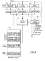
- Referring now to Figure 1 which shows a typical prior art CRT timer,
registers 1 to 12 are provided, one for each event for which a timing signal is required. Associated withregisters 1 to 12 arecomparators 13 to 25 respectively. The registers and associated comparators are grouped together into three groups in accordance with whether the timing signal is dependent upon character position, row position or line position. Within this specification, the character position is the horizontal position along the horizontal raster scan line. Thus if the CRT display can display up to 80 characters across its screen, there will be up to 80 screen character positions plus a further number of non-displayable character positions (for example 20) to allow for line flyback. The row position is the vertical position of the row of characters, for example it may be possible to display up to 24 rows of characters. The line position is the vertical position of the scan line: for example if each row of displayed characters requires 12 raster scan lines, 24 rows would require 288 scan lines. -
Character counter 25, incremented by an oscillator online 26, will contain the current horizontal position of the electron beam as it raster scans across the screen.Row counter 27 will contain the current row position andline counter 28 will contain the current scan line position. By means of adata bus 29, various values can be entered into theregisters 1 to 12. - Typical of events which depend on the horizontal position of the beam, i.e. the character count, are horizontal synchronization start, horizontal synchronization stop, end of scan line etc and the appropriate counts at which these events are to occur are loaded into
registers 1 to 4. When a comparison is detected, a signal on theoutput lines 30 to 32 will indicate the timing of that event. The end-of-line output 32 is used to reset thecharacter counter 25 and to increment theline counter 28. Figure 1 is somewhat simplified in showingoutput line 32 incrementing row counter 27: in practice the row counter would be incremented at the end of a scan line only if that were the last scan line (for example the eighth) of a character row. - Similarly, counts of events which depend on the row count or the scan line count are loaded on
data bus 29 into appropriate registers. Whenever the appropriate counts are detected, an output is signalled onlines 33 to 38. Although this circuit arrangement works, it has some drawbacks. It is relatively expensive since each programmable time requires a register and comparator. Also, once the basic display characteristics have been fixed, it might be difficult, if not impossible, to add new features rather than re-time existing features. - However, the timing circuit shown in Figure 2 only requires three comparators, one for each group of events and, instead of separate registers, makes use of a register stack. This makes for a much more versatile arrangement which is also more suitable for implementation in t large scale integration (LSI).
- As shown in Figure 2, three
counters 40 to 42 contain the current character, line and row counts respectively.Character counter 40 is incremented by an oscillator on line 43. Every so often, in fact when it is reset,counter 40 will increment line counter 41 online 44. Similarly every few scan lines,row counter 42 will be incremented. Each counter has associated therewith acomparator 45, 46 or 47. Thuscomparator 45 is used for deriving the timing of character events, comparator 46 for line events and comparator.47 for row events. - All events that require timing are loaded into a
register stack 48 in the sequence in which they will occur. Each entry in thestack 48 has flags to identify the event being timed. In operation, address circuits 49 cause the first entry to be presented to thecomparators 45 and when a comparison is achieved, the flags in that entry are decoded inflag decoder 50 to indicate the nature of the event, for example H sync start. Each time a compare is achieved, the address circuitry 49 advances to present the next entry in theregister stack 48 to the comparator. - Stack entries may include events that call for internal operations such as resetting the character or other counter. Similarly a stack entry may call for a different area of the stack (that is non-sequential), for example that containing line or row timings, to be compared with another counter, the line or row counter. In this way, all programmable events may be contained in a single area of random access memory. The arrangement shown is preferred since it is convenient to group together the character, line or row dependent events. However, it is possible to use only one counter and one comparator since all events can be timed on the character counts if this runs from 0 at the top left of the screen to the maximum count at the bottom right. In this event every event would be loaded strictly in sequence.
- It may be convenient to provide a default set of timings for use when the programmable times are not loaded in the register stack. In this event a small read only store (ROS), not shown, could provide the default set. When in the default state, for example immediately after power on of the display, the address circuitry 49 would ensure that only the events coded in the ROS are presented to the comparators.
- Figure 3 shows the format of the entries in the stack register for character events. Eight events may occur during a scan line:-
- Horizontal synchronization start/stop
- Blanking start/stop
- Scroll area enter/leave
- Frame and slice position check
- Line end
- Eight locations in the stack are reserved for these horizontal or character events and are coded as shown in Figure 3. When the character number in
fields 0 to 7 compares with the character counter, the flags infields 11 to 15 are examined indecoder 50 and the appropriate action taken. For example a "1" on the sync flag will cause a 'set' to a sync latch, not shown, and a '0' a reset. The End of Line flag causes thecharacter counter 40 to reset. The Do Line and Slice flag causes a compare of the line stack with the line counter 41 followed by similar compares on the slice and scrolled slice counters. Several characters with no line events should follow the Do Line and Slice event. - A similar coding scheme applies to Figure 4 which shows Vertical Frame or Line Events and Figure 5 which shows Vertical Slice or Row Events.
- Once per line, under control from the character Event stack, the
row counter 42 is compared with the slice or row event stack. If the number compares, the flags are inspected and the appropriate latches (not shown) set or resent. If scroll offset is active therow counter 42 is reset and scroll control logic (not shown) is signalled to indicate that a row boundary has been crossed. The row counter is also compared with the row event stack once per scan line to determine the events active on the row scan line. These events (e.g. underscore) are held in separate latches (not shown). - As the Timing and Sync circuit relies on the sequential retrieval of events from the stack, the microcode or other control logic must ensure that the stack is loaded in the corresponding sequence. Hence when changing event timings, some re-ordering may become necessary.
- The following is a list of the parameters that may be programmed within the timer.
-
- 1. Horizontal Scan Line Length Total number of characters per scan line, i.e. defines horizontal sync period. (8 bits allowing up to 256 characters including flyback.)
- 2. Horizontal Sync Start Position Character number of sync start (8 bits).
- 3. Horizontal Sync Stop Position Character number of sync stop (8 bits).
- 4. Horizontal Margin Start Position Defines the start of the horizontal blanking (8 bits).
- 5. Horizontal Margin Stop Position Defines the stop of the horizontal blanking (8 bits).
- 6. Vertical Display Total number of scan lines in the display, i.e. defines the vertical sync period (10 bits allowing up to 1024 lines including flyback).
- 7. Vertical Sync Start Position Line number of the start of the vertical sync pulse (10 bits).
- 8. Vertical Sync Stop Position Line number of the stop of vertical sync (10 bits).
- 9. Vertical Margin Start Position Line number defining the start of vertical blanking (10 bits).
- 10. Vertical Margin Stop Position Defines the stop of the vertical blanking (10 bits).
- 11. Number of Scan Lines Per Character Row Defines the total number of scan lines per row (5 bits).
- 12. Underscore Line Defines line number on which the underscore is to appear (5 bits).
- 13. Cursor Start Line Defines line number on which the reverse cursor is to start (5 bits).
- 14. Cursor Line Defines line number on which the reverse cursor is to stop or on which the normal cursor is to be drawn (5 bits).
- 15. Scroll Offset Defines number of scan lines a scroll counter is offset from the main row counter (5 bits).
- a 16. Scroll Partition Start Character Defines character number on which the partition to be scrolled starts (8 bits).
- 17. Scroll Partition Stop Character Defines character number on which the partition to be scrolled stops (8 bits).
- 18. Scroll Partition Start Line Defines the line number on which the partition to be scrolled starts (10 bits).
- 19. Scroll Partition Stop Line Defines the line number on which the partition to be scrolled stops (10 bits).
- The various analogue circuits which would co-act with the timer shown in Figure 2 are not shown since they do not form part of the present invention. Similarly no details of the overall control logic of the display is shown. Typically, however, the display could be controlled by a microprocessor in a similar manner to the well known IBM 8775 display station. However, the invention is not limited to use in such a microprocessor-controlled display.
Claims (6)
Priority Applications (4)
| Application Number | Priority Date | Filing Date | Title |
|---|---|---|---|
| DE8383303792T DE3370090D1 (en) | 1983-06-30 | 1983-06-30 | Programmable timing circuit for cathode ray tube |
| EP83303792A EP0130247B1 (en) | 1983-06-30 | 1983-06-30 | Programmable timing circuit for cathode ray tube |
| US06/562,949 US4644340A (en) | 1983-06-30 | 1983-12-19 | Programmable timing circuit for cathode ray tube |
| JP59049446A JPS604982A (en) | 1983-06-30 | 1984-03-16 | Programmable timing circuit for crt |
Applications Claiming Priority (1)
| Application Number | Priority Date | Filing Date | Title |
|---|---|---|---|
| EP83303792A EP0130247B1 (en) | 1983-06-30 | 1983-06-30 | Programmable timing circuit for cathode ray tube |
Publications (2)
| Publication Number | Publication Date |
|---|---|
| EP0130247A1 true EP0130247A1 (en) | 1985-01-09 |
| EP0130247B1 EP0130247B1 (en) | 1987-03-04 |
Family
ID=8191201
Family Applications (1)
| Application Number | Title | Priority Date | Filing Date |
|---|---|---|---|
| EP83303792A Expired EP0130247B1 (en) | 1983-06-30 | 1983-06-30 | Programmable timing circuit for cathode ray tube |
Country Status (4)
| Country | Link |
|---|---|
| US (1) | US4644340A (en) |
| EP (1) | EP0130247B1 (en) |
| JP (1) | JPS604982A (en) |
| DE (1) | DE3370090D1 (en) |
Cited By (1)
| Publication number | Priority date | Publication date | Assignee | Title |
|---|---|---|---|---|
| EP0353725A2 (en) * | 1988-08-04 | 1990-02-07 | Honeywell Inc. | Raster deflection signal generation apparatus |
Families Citing this family (3)
| Publication number | Priority date | Publication date | Assignee | Title |
|---|---|---|---|---|
| US4837563A (en) * | 1987-02-12 | 1989-06-06 | International Business Machine Corporation | Graphics display system function circuit |
| JP2628590B2 (en) * | 1990-10-11 | 1997-07-09 | シャープ株式会社 | Scan line position detector |
| US10416703B2 (en) * | 2017-08-10 | 2019-09-17 | Ambiq Micro, Inc. | Counter/timer array for generation of complex patterns independent of software control |
Citations (1)
| Publication number | Priority date | Publication date | Assignee | Title |
|---|---|---|---|---|
| US4232374A (en) * | 1977-08-11 | 1980-11-04 | Umtech, Inc. | Segment ordering for television receiver control unit |
Family Cites Families (4)
| Publication number | Priority date | Publication date | Assignee | Title |
|---|---|---|---|---|
| US3396377A (en) * | 1964-06-29 | 1968-08-06 | Gen Electric | Display data processor |
| US3522597A (en) * | 1965-11-19 | 1970-08-04 | Ibm | Execution plotter |
| JPS5742081A (en) * | 1980-08-28 | 1982-03-09 | Tokyo Shibaura Electric Co | Display unit |
| JPS5745587A (en) * | 1980-08-30 | 1982-03-15 | Fujitsu Ltd | Figure enlargement display unit |
-
1983
- 1983-06-30 EP EP83303792A patent/EP0130247B1/en not_active Expired
- 1983-06-30 DE DE8383303792T patent/DE3370090D1/en not_active Expired
- 1983-12-19 US US06/562,949 patent/US4644340A/en not_active Expired - Fee Related
-
1984
- 1984-03-16 JP JP59049446A patent/JPS604982A/en active Granted
Patent Citations (1)
| Publication number | Priority date | Publication date | Assignee | Title |
|---|---|---|---|---|
| US4232374A (en) * | 1977-08-11 | 1980-11-04 | Umtech, Inc. | Segment ordering for television receiver control unit |
Non-Patent Citations (2)
| Title |
|---|
| IBM TECHNICAL DISCLOSURE BULLETIN, vol. 19, no. 3, August 1976, pages 1081-1084, New York, US * |
| IEEE TRANSACTIONS ON CONSUMER ELECTRONICS, vol. CE-27, no. 4, November 1981, pages 612-625, IEEE, New York, US * |
Cited By (2)
| Publication number | Priority date | Publication date | Assignee | Title |
|---|---|---|---|---|
| EP0353725A2 (en) * | 1988-08-04 | 1990-02-07 | Honeywell Inc. | Raster deflection signal generation apparatus |
| EP0353725A3 (en) * | 1988-08-04 | 1990-05-16 | Honeywell Inc. | Raster deflection signal generation apparatus |
Also Published As
| Publication number | Publication date |
|---|---|
| DE3370090D1 (en) | 1987-04-09 |
| JPS604982A (en) | 1985-01-11 |
| JPH0320756B2 (en) | 1991-03-20 |
| EP0130247B1 (en) | 1987-03-04 |
| US4644340A (en) | 1987-02-17 |
Similar Documents
| Publication | Publication Date | Title |
|---|---|---|
| US4425559A (en) | Method and apparatus for generating line segments and polygonal areas on a raster-type display | |
| US4119955A (en) | Circuit for display, such as video game display | |
| US4486856A (en) | Cache memory and control circuit | |
| US4873514A (en) | Video display system for scrolling text in selected portions of a display | |
| US3895375A (en) | Display apparatus with facility for underlining and striking out characters | |
| EP0139095A3 (en) | Display selection in a raster scan display system | |
| US4011556A (en) | Graphic display device | |
| US4119953A (en) | Timesharing programmable display system | |
| US4644340A (en) | Programmable timing circuit for cathode ray tube | |
| EP0004797A2 (en) | Video display control apparatus | |
| EP0281008B1 (en) | Digital data display apparatus | |
| EP0123896A2 (en) | Character and video mode control circuit | |
| US6559838B1 (en) | Power management in a monitor | |
| US3803584A (en) | Display system | |
| CA1227297A (en) | Oscilloscope | |
| US3930250A (en) | Synchronizing system for refresh memory | |
| EP0110180A1 (en) | Storage apparatus for video data | |
| US4660154A (en) | Variable size and position dialog area display system | |
| US4980605A (en) | Oscilloscope triggering control circuit | |
| EP0282145B1 (en) | Video display apparatus | |
| CA1236601A (en) | Window borderline generating circuit for crt display | |
| US5045845A (en) | Image processing apparatus | |
| JPS62263471A (en) | Method of displaying logic signal | |
| US4028724A (en) | Read/write character generator memory loading method | |
| JP3461063B2 (en) | Character display device |
Legal Events
| Date | Code | Title | Description |
|---|---|---|---|
| PUAI | Public reference made under article 153(3) epc to a published international application that has entered the european phase |
Free format text: ORIGINAL CODE: 0009012 |
|
| AK | Designated contracting states |
Designated state(s): DE FR GB |
|
| 17P | Request for examination filed |
Effective date: 19841123 |
|
| GRAA | (expected) grant |
Free format text: ORIGINAL CODE: 0009210 |
|
| AK | Designated contracting states |
Kind code of ref document: B1 Designated state(s): DE FR GB |
|
| ET | Fr: translation filed | ||
| REF | Corresponds to: |
Ref document number: 3370090 Country of ref document: DE Date of ref document: 19870409 |
|
| PLBE | No opposition filed within time limit |
Free format text: ORIGINAL CODE: 0009261 |
|
| STAA | Information on the status of an ep patent application or granted ep patent |
Free format text: STATUS: NO OPPOSITION FILED WITHIN TIME LIMIT |
|
| 26N | No opposition filed | ||
| PGFP | Annual fee paid to national office [announced via postgrant information from national office to epo] |
Ref country code: GB Payment date: 19920506 Year of fee payment: 10 |
|
| PGFP | Annual fee paid to national office [announced via postgrant information from national office to epo] |
Ref country code: FR Payment date: 19920601 Year of fee payment: 10 |
|
| PGFP | Annual fee paid to national office [announced via postgrant information from national office to epo] |
Ref country code: DE Payment date: 19920619 Year of fee payment: 10 |
|
| PG25 | Lapsed in a contracting state [announced via postgrant information from national office to epo] |
Ref country code: GB Effective date: 19930630 |
|
| GBPC | Gb: european patent ceased through non-payment of renewal fee |
Effective date: 19930630 |
|
| PG25 | Lapsed in a contracting state [announced via postgrant information from national office to epo] |
Ref country code: FR Effective date: 19940228 |
|
| PG25 | Lapsed in a contracting state [announced via postgrant information from national office to epo] |
Ref country code: DE Effective date: 19940301 |
|
| REG | Reference to a national code |
Ref country code: FR Ref legal event code: ST |