EP0352935A2 - Pipelineprozessor - Google Patents
Pipelineprozessor Download PDFInfo
- Publication number
- EP0352935A2 EP0352935A2 EP89307058A EP89307058A EP0352935A2 EP 0352935 A2 EP0352935 A2 EP 0352935A2 EP 89307058 A EP89307058 A EP 89307058A EP 89307058 A EP89307058 A EP 89307058A EP 0352935 A2 EP0352935 A2 EP 0352935A2
- Authority
- EP
- European Patent Office
- Prior art keywords
- pipeline
- instruction
- stream
- instructions
- units
- Prior art date
- Legal status (The legal status is an assumption and is not a legal conclusion. Google has not performed a legal analysis and makes no representation as to the accuracy of the status listed.)
- Granted
Links
- 238000012545 processing Methods 0.000 claims abstract description 15
- 238000000034 method Methods 0.000 claims abstract description 7
- 125000004122 cyclic group Chemical group 0.000 claims 1
- 238000001514 detection method Methods 0.000 claims 1
- 230000006870 function Effects 0.000 description 8
- 230000000977 initiatory effect Effects 0.000 description 5
- 230000000694 effects Effects 0.000 description 3
- 238000004891 communication Methods 0.000 description 2
- 238000012937 correction Methods 0.000 description 1
- 238000010586 diagram Methods 0.000 description 1
- 238000006073 displacement reaction Methods 0.000 description 1
- 230000009977 dual effect Effects 0.000 description 1
- 238000004519 manufacturing process Methods 0.000 description 1
- 238000011084 recovery Methods 0.000 description 1
- 238000012360 testing method Methods 0.000 description 1
Images


Classifications
-
- G—PHYSICS
- G06—COMPUTING; CALCULATING OR COUNTING
- G06F—ELECTRIC DIGITAL DATA PROCESSING
- G06F9/00—Arrangements for program control, e.g. control units
- G06F9/06—Arrangements for program control, e.g. control units using stored programs, i.e. using an internal store of processing equipment to receive or retain programs
- G06F9/30—Arrangements for executing machine instructions, e.g. instruction decode
- G06F9/38—Concurrent instruction execution, e.g. pipeline, look ahead
- G06F9/3861—Recovery, e.g. branch miss-prediction, exception handling
- G06F9/3865—Recovery, e.g. branch miss-prediction, exception handling using deferred exception handling, e.g. exception flags
-
- G—PHYSICS
- G06—COMPUTING; CALCULATING OR COUNTING
- G06F—ELECTRIC DIGITAL DATA PROCESSING
- G06F9/00—Arrangements for program control, e.g. control units
- G06F9/06—Arrangements for program control, e.g. control units using stored programs, i.e. using an internal store of processing equipment to receive or retain programs
- G06F9/30—Arrangements for executing machine instructions, e.g. instruction decode
- G06F9/30145—Instruction analysis, e.g. decoding, instruction word fields
- G06F9/3016—Decoding the operand specifier, e.g. specifier format
- G06F9/30167—Decoding the operand specifier, e.g. specifier format of immediate specifier, e.g. constants
-
- G—PHYSICS
- G06—COMPUTING; CALCULATING OR COUNTING
- G06F—ELECTRIC DIGITAL DATA PROCESSING
- G06F9/00—Arrangements for program control, e.g. control units
- G06F9/06—Arrangements for program control, e.g. control units using stored programs, i.e. using an internal store of processing equipment to receive or retain programs
- G06F9/30—Arrangements for executing machine instructions, e.g. instruction decode
- G06F9/38—Concurrent instruction execution, e.g. pipeline, look ahead
- G06F9/3836—Instruction issuing, e.g. dynamic instruction scheduling or out of order instruction execution
- G06F9/3851—Instruction issuing, e.g. dynamic instruction scheduling or out of order instruction execution from multiple instruction streams, e.g. multistreaming
-
- G—PHYSICS
- G06—COMPUTING; CALCULATING OR COUNTING
- G06F—ELECTRIC DIGITAL DATA PROCESSING
- G06F9/00—Arrangements for program control, e.g. control units
- G06F9/06—Arrangements for program control, e.g. control units using stored programs, i.e. using an internal store of processing equipment to receive or retain programs
- G06F9/30—Arrangements for executing machine instructions, e.g. instruction decode
- G06F9/38—Concurrent instruction execution, e.g. pipeline, look ahead
- G06F9/3861—Recovery, e.g. branch miss-prediction, exception handling
- G06F9/3863—Recovery, e.g. branch miss-prediction, exception handling using multiple copies of the architectural state, e.g. shadow registers
-
- G—PHYSICS
- G06—COMPUTING; CALCULATING OR COUNTING
- G06F—ELECTRIC DIGITAL DATA PROCESSING
- G06F9/00—Arrangements for program control, e.g. control units
- G06F9/06—Arrangements for program control, e.g. control units using stored programs, i.e. using an internal store of processing equipment to receive or retain programs
- G06F9/30—Arrangements for executing machine instructions, e.g. instruction decode
- G06F9/38—Concurrent instruction execution, e.g. pipeline, look ahead
- G06F9/3867—Concurrent instruction execution, e.g. pipeline, look ahead using instruction pipelines
- G06F9/3875—Pipelining a single stage, e.g. superpipelining
-
- G—PHYSICS
- G06—COMPUTING; CALCULATING OR COUNTING
- G06F—ELECTRIC DIGITAL DATA PROCESSING
- G06F9/00—Arrangements for program control, e.g. control units
- G06F9/06—Arrangements for program control, e.g. control units using stored programs, i.e. using an internal store of processing equipment to receive or retain programs
- G06F9/30—Arrangements for executing machine instructions, e.g. instruction decode
- G06F9/38—Concurrent instruction execution, e.g. pipeline, look ahead
- G06F9/3885—Concurrent instruction execution, e.g. pipeline, look ahead using a plurality of independent parallel functional units
- G06F9/3889—Concurrent instruction execution, e.g. pipeline, look ahead using a plurality of independent parallel functional units controlled by multiple instructions, e.g. MIMD, decoupled access or execute
Definitions
- This invention relates to data processing apparatus of the kind having a series of stages which execute successive instructions in an overlapped manner.
- Such apparatus is usually referred to as a pipelined processor.
- One object of the present invention is to provide a novel organisation for such a pipelined processor, which facilitates the co-ordination and control of a large number of pipeline stages.
- data processing apparatus comprising:
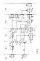
- the data processing apparatus comprises a series of pipeline units as follows: an instruction scheduler 10, an upper pipeline unit 11, a fast data slave store 12, and a lower pipeline unit 13.
- the pipeline units 10-13 are interconnected by parameter files as follows: an instruction parameter file IPF, an address parameter file APF, and an operand parameter file OPF. These allow instruction parameters to be passed between the pipeline units.
- the scheduler 10 has a fast code slave 14 associated with it, for holding copies of instructions for access by the scheduler.
- the system also includes a main store 15 of larger size but slower access speed than the slave stores, 12, 14, and a slow slave store 16 of size and speed intermediate between those of the main store and the fast slaves.
- the fast slaves, the slow slave, and the main store form a three-level storage hierarchy.
- the scheduler 10 comprises two scheduler units 10A and 10B, for scheduling two separate streams of instructions, referred to as stream A and stream B.
- Stream A is dedicated to the main processing workload of the system.
- Stream B handles events that are independent of this main processing workload, such as managing input/output activity, and communication with other processors.
- the provision of two independent streams allows more effective use of the hardware of the system. For example, as will be shown, when one stream is held up for some reason, the other stream can continue processing, so that the hardware is not idle.
- Each of the scheduler units 10A, 10B generates a sequence of instruction addresses, for retrieving instructions from the code slave 14. If the required instruction is not in the code slave, it is retrieved from the slow slave 16 or from the main store 15. The retrieved instructions are written into the IPF. Each instruction is accompanied by a program counter value PC which is also written into a portion of the IPF referred to as IPF.pc.
- the IPF has dual ports, so that the scheduler units 10A, 10B can load the IPF simultaneously.
- Each of the parameter files IPF, APF and OPF (as well as another parameter file TPF to be described later) comprises sixteen registers, and can therefore hold parameters for up to sixteen different instructions at various stages of execution.
- the set of registers relating to a particular instruction is referred to as a slot: that is, each slot comprises a corresponding register from each of the register files.
- Ten of the slots are allocated to stream A and six to stream B.
- an instruction When an instruction is initially entered into the IPF from the scheduler, it is assigned a slot i.e. it is assigned a register in IPF and a corresponding register in each of the other parameter files. The instruction then retains this slot until it has been successfully executed by all stages of each pipeline unit, whereupon the slot is released so that it is available for another instruction from the scheduler. As an instruction passes down the pipeline, the slot number assigned to that instruction is passed down the pipeline with it, so that at each pipeline stage the appropriate register in the parameter file can be accessed.
- the upper pipeline 11 reads instructions from the IPF and processes them, so as to calculate the address of the required operand for the instruction. This may, for example, involve adding a displacement value to a base address held in an internal register, such as a local name base register. Alternatively, the address may be a literal value held in the instruction.
- the operand address is placed in the APF in the slot appropriate to the instruction in question.
- the data slave 12 when it is free, reads an address from the APF and retrieves the required operand, if it is present in the data slave, or alternatively initiates fetching of the operand from the slow slave or the main store.
- the retrieved operand is placed in the OPF in the slot appropriate to the instruction in question. Additionally, data from the slave may be returned to the upper pipeline so as to update one of the internal registers in that unit.
- the lower pipeline 13 reads the operand from the OPF and performs the required operation on it as specified by the instruction. For example, this may involve adding the operand to the contents of an accumulator register.
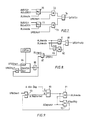
- the upper pipeline unit includes five pipeline stages referred to as UPO - UP4.
- the first stage UPO contains logic, to be described below, for selecting a slot from the IPF, so as to initiate processing of the instruction in that slot.
- the upper pipeline may detect that the instruction cannot be successfully completed yet, because of a dependency on an earlier instruction. In this case, the instruction is abandoned. However instructions following the abandoned instruction are allowed to continue running in a special mode called look-ahead mode, the purpose of which is to allow operands for the instruction to be prefetched, if necessary, into the fast data slave. Such look aheads are allowed only if they do not generate any further dependencies.
- the look-ahead mode can be initiated for streams A and B independently. When stream A is in look-ahead mode but not stream B, then stream B is given priority. When the dependency has been resolved, the stream is returned to normal non-look-ahead mode, and the abandoned instruction is restarted in the upper pipeline.
- UP1 comprises a decoder 20 which decodes the instruction from the selected slot to generate control signals for UP2, these being stored in a pipeline register 21.
- the decoder 20 also produces an output signal which is passed to UP2 for further decoding, by way of a register 23.
- UP2 contains a set of registers 24 which represent local copies of the registers specified by the instruction set of the system. The definitive copies of these registers are actually in the lower pipeline. UP2 also contains a multiplexing circuit 25, which is controlled by the value in register 21 and which selects input data for the registers 24 from one of the following sources:
- UP2 also contains a decoder 26 which further decodes the contents of register 23 to produce a set of control signals for UP3, these being stored in a register 27.
- the decoder also produces a function code F which is stored in a register 28.
- UP3 comprises a multiplexing circuit 29 which selects input data for a set of arithmetic registers 210, under control of the value in register 27.
- the input data is selected from the following sources:
- UP3 also contains a register 215 which passes the function code F to UP4.
- the function code F is also passed from UP3 to the parameter files APF and OPF where it is stored in the appropriate slot.
- the portions of these parameter files which store the function code are referred to as APF.F and OPF.F.
- UP4 contains an arithmetic and logic unit (ALU) 216, which performs an operation on the contents of the registers 210 under control of the function code F in the register 215. The result of the operation is passed to the APF, where it is written into the appropriate slot.
- ALU arithmetic and logic unit
- the address generated in UP4 may be checked for architectural validity. Any error will cause a later unsuccessful termination of this slot.
- the data slave includes five pipeline stages DSO - DS4.
- the first stage DSO comprises a priority logic circuit for selecting the next slot from the APF to be handled by the data slave.
- DS1 contains a decoder 30 which decodes the address selected from APF, to produce a byte shift value indicating the alignment of the required data item within a 32-byte block.
- the address and the byte shift value are passed to DS2 by way of registers 31 and 32.
- DS2 comprises a contents - addressable memory (CAM) 33, which holds the addresses of data items currently in the data slave.
- the CAM 33 receives the operand address from DS1, and compares it with all the addresses held in the CAM. If there is a match, the CAM produces a signal VHIT, and at the same time outputs a tag value indicating which 32-byte block of the data slave the required item is held in.
- the tag value is passed to DS3 by way of a register 34.
- the data slave triggers an access to the slow slave, which will cause the data to be fetched, either from the slow slave or the main store, and loaded into the data slave.
- the DS2 also includes a byte alignment circuit 35 which receives a data item W from the lower pipeline and aligns it according to the byte shift value held in the register 32.
- the aligned data item is stored in a register 36.
- DS2 also includes registers 37 and 38 which receive data items returned to the data slave from the main store and slow slave respectively.
- DS3 comprises a random-access memory (RAM) 39 which holds a number of individually addressable 32-byte blocks of data.
- the RAM is addressed by the tag value from register 34.
- Data can be written into the RAM, by way of a multiplexer 310, from any of the registers 36, 37 and 38. Alternatively, a block of data can be read out of the RAM and passed to DS4 by way of a register 311.
- DS4 comprises a byte alignment circuit 312. This is controlled by a byte shift value, received from the decoder 40 by way of pipeline registers 32, 313 and 314.
- the alignment circuit 312 selects the required data item from the block held in register 311, and passes it to the OPF.
- the selected data item is also supplied to the upper and lower pipelines as data signal RD.
- the lower pipeline includes four pipeline stages LPO - LP3
- the first stage LPO contains a priority logic, to be described, for selecting the next slot from OPF to be handled by the lower pipeline.
- the execution of an instruction in the lower pipeline may be started as soon as it is certain that the operand for it will be available from the data slave in time for use at stage LP2 of the lower pipeline.
- an instruction may be started in the lower pipeline while the data item is actually being retrieved from the data slave.
- the data signal RD from the data slave is used directly in LP1, bypassing OPF.
- operations of the pipeline stages of the data slave and the lower pipeline can be overlapped. This is important, since it reduces the total transit time of instructions through the overall pipeline.
- LP1 comprises a control store 40 having an address input which receives the function code F from the selected slot of OPF.f, by way of a multiplexer 41.
- the output of the control store 40 comprises a control code, and a next address value.
- the control code is passed to LP2 by way of a register 42.
- the next address value is fed back to a register 43 in LPO, and can then be selected by the multiplexer 41 so as to address another location in the control store 40.
- the control store 40 can produce a sequence of control codes for the lower pipeline.
- control store At the end of the sequence of control codes, the control store produces an end of sequence signal, which tells the priority logic in stage LP0 to select a new slot, and switches the multiplexer 41 so as to select the next function code from OPF.f, thus initiating a new sequence.
- LP1 also includes a set of arithmetic registers 44. Data can be loaded into these registers by way of a multiplexing circuit 45 from either the following sources:
- Multiplexer 45 can also take bypass data from registers 47 or ALU 46, where that data has not yet been written into the required register 411.
- LP2 comprises an arithmetic and logic unit (ALU) 46 which performs an operation on the contents of registers 44 as specified by the control held in register 42. The result of this operation is passed to LP3 by way of registers 47 and 48.
- ALU arithmetic and logic unit
- TPF termination parameter file
- TPF comprises sixteen registers, one for each slot. Whenever an instruction detects a problem in execution in any of the pipeline units, an indicator is set in the slot of TPF corresponding to that instruction.
- LP3 includes a condition logic circuit 412 which receives the output of the register 48 and a control signal from the control store 40 by way of registers 42 and 410.
- the circuit 412 performs tests to detect whether a jump condition specified by the instruction has been satisfied, e.g. whether an accumulator register is zero. If the jump condition is satisfied, the circuit 412 produces a jump signal JCON for the scheduler 10.
- LP3 contains finish logic 49, which receives a control signal from the condition logic 412 to indicate whether any problems have been detected during execution in LP2.
- the logic 49 examines the signal and the contents of TPF corresponding to the instruction, and determines whether this instruction has encountered any problems during execution. When successful completion is detected, the circuit produces one of two signals AFinOK or BFinOK, depending on which stream the instruction is in. The slot allocated to the instruction is then released for re-use.
- LP3 also includes a set of registers 411 which represents the definitive copies of the registers specified by the instruction set of the system. These registers receive data from the register 47. The registers 411 are loaded from register 47 only when the finish logic 49 indicates that this slot is completing successfully. In this way, the current process state, as defined in registers 411, is not corrupted by any errors in the execution of an instruction. The output of the registers 411 provides the correction signal UP.CORR which can be fed back to the upper pipeline if required, to correct the local copies of the registers held there.
- the output of the register 47 also provides the signal W to the data slave, and the signal V to the upper pipeline.
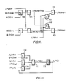
- Counter 50 produces a signal ALdSlt which indicates the next slot in the IPF to be loaded by an A-stream instruction from the scheduler.
- the counter 50 is incremented by a signal APiLd whenever an A-stream instruction is loaded into the IPF.
- the slots in the IPF are allocated sequentially to successive instructions.
- Counter 51 produces a signal AUStSlt which indicates the next A-stream slot to be started in the upper pipeline UP in normal mode (i.e. non-look-ahead mode).
- counter 52 produces a signal AULaStSlt which indicates the next A-stream slot to be started in the upper pipeline in look-ahead mode.
- a look-ahead signal ALAmode is false.
- a signal UPAStart goes true. This enables an AND gate 56 , which increments the counter 51.
- the counter 51 selects A-stream instructions from successive slots of the IPF, so as to initiate processing of these instructions in the upper pipeline.
- an AND gate 57 and an OR gate 58 are enabled, which increments the counter 52.
- the two counters 51, 52 are incremented in step with each other.
- ALAmode In look-ahead mode, ALAmode is true, and so the AND gate 56 is disabled, which prevents the counter 51 from being incremented.
- an AND gate 59 is enabled, and this increments the counter 52.
- the counter 52 continues counting, so as to continue to select successive instructions from the IPF for starting in the upper pipeline.
- the counter 51 retains the slot number of the instruction which was abandoned.
- Counter 53 produces a signal ALStSlt which indicates the next A-stream slot to be started in the lower pipeline LP. This counter 53 is incremented by a signal LPAStart whenever an A-stream instruction is started in the lower pipeline. Thus, the instructions are started sequentially in the lower pipeline.
- the counter 54 produces a signal AEldSlt which indicates the slot holding the eldest A-stream instruction currently in the pipeline. Instructions are completed in strictly chronological order, and hence this signal indicates the next A-stream instruction which is due to finish execution in the lower pipeline.
- the counter 54 is incremented by a signal AFinOK which indicates that an A-stream instruction has successfully completed execution in the lower pipeline. This releases the slot.
- the contents of the counters 50 and 51 are compared, to produce a signal AUAllSt, which indicates that all the A-stream instructions currently in the IPF have now been started in normal mode.
- the contents of the counters 50 and 52 are compared, to produce a signal AULaAllSt, which indicates that all the A-stream instructions currently in the IPF have now been started, with possibly some of them in look-ahead mode.
- the contents of the counters 50 and 54 are compared to produce a signal AIpfFull which indicates that all the A-stream slots in the IPF are now full. This prevents any further A-stream instructions from being loaded into the IPF.
- Figure 6 to 8 show the control logic for starting instructions in the upper pipeline.
- a multiplexer 60 selects either AUAllSt or AULaAllSt according to whether the signal ALAmode is false or true.
- the inverse of the output of the multiplexer 60 provides a signal AIpfRdy which indicates that there is at least one A-stream instruction in the IPF ready to be started in the upper pipeline.
- a similar signal BIpfRdY is produced for the B-stream.
- the signal AIpfRdy is fed to one input of an AND gate 61, which produces a signal UPAStart, for initiating an A-stream instruction in the upper pipeline.
- the other input of this AND gate receives the output of an OR gate 62, which receives the inverse of BIpfRdy and the inverse of a priority signal UPBStPrefd.
- BIpfRdy is fed to one input of an AND gate 63, which produces a signal UPBStart, for initiating a B-stream instruction in the upper pipeline.
- the other input of this AND gate receives the output of an OR gate 64, which receives UPBStPrefd and the inverse AIpfRdy.
- a multiplexer 70 selects either AUStSlt or AULaStSlt according to whether ALAmode is false or true. The output of this multiplexer therefore indicates the slot number of the next A-stream instruction to be started in the upper pipeline, in normal or look-ahead mode as the case may be.
- a similar multiplexer 71 is provided for the B-stream.
- the outputs of the multiplexers are gated by way of AND gates 72, 73 to an OR gate 74, the output of which provides a signal IpfRdSlt. This signal is used to address the IPF, for reading out the next instruction for starting in the upper pipeline.
- the AND gates 72, 73 are controlled by signals UPAStart and UPBStart as shown, so as to select the slot number for the A stream or B stream as required.
- this shows the logic for producing the signal UPBStprefd which indicates that the B stream is preferred for starting in the upper pipeline.
- UPBStprefd is derived from an OR gate 80 which receives the output of two AND gates 81 and 82.
- AND gate 81 receives the signal ALAmode and the inverse of the corresponding signal BLAmode for the B-stream.
- Gate 82 receives a signal UPBPri, and the output of an equivalence gate 83, which combines ALAmode and BLAmode.
- the signal UPBStPrefd gives preference to the stream that is in normal mode. If, on the other hand, both streams are in the same mode, then preference is given to the A stream or the B stream according to whether UPBPri is false or true.
- the signal UPBPri is produced as follows.
- a counter 84 is loaded with a preset value USPlim whenever a B-stream instruction is started in the upper pipeline, as indicated by UPBStart. The counter is then decremented whenever an A-stream instruction is started, as indicated by UPAStart. When the count reaches zero an AND gate 85 is enabled, which in turn enables OR gate 87, so as to make UPBPri true.
- the values of USPlim can be preset to a value such as to achieve a desired balance between the two streams.
- the OR gate 87 also receives a signal BUrgent, which gives priority to the B-stream when pending input/output activity or inter-processor communication has become critical, over-riding the effect of the counter 84.
- this shows the logic for controlling the look ahead mode.
- AAbnDep sets a flip flop 90.
- the signal ADepWait goes false again when it is detected that the dependency has now been resolved, or is likely to be resolved shortly. This disables AND gate 91, making ALAmode false, and at the same time enables an AND gate 92, producing a signal AReStRdy.
- the signals UPAStart and ARestRdy enable an AND gate 93, producing a signal ARestarted, which resets the flip flop 90.
- an abandoned instruction may be restarted before the dependency has actually been resolved. For example, consider the case where an instruction has been abandoned because it requires to read data from a register that has not yet been written from the slave output data RD of an earlier instruction. In this case, the signal ADepWait will go false as soon as an access is initiated in the data slave to retrieve the required data. Thus, the restarted instruction will start running in the upper pipeline in parallel with the access to the data slave by the earlier instruction. By the time the restarted instruction requires to read the data, it is likely that the data will have been accessed from the data slave, and so execution will proceed normally. However, if the required data is not in the data slave, the restarted instruction will be abandoned again, and look-ahead mode is re-activated.
- Figures 10 and 11 show the control logic for starting instructions in the lower pipeline LP.
- a signal ADsDone is produced, to indicate that the required data slave access (if any) for the A stream has been completed or is expected to be completed shortly.
- This signal consists of ten bits, one for each a stream slot. These ten bits are applied to a multiplexer 100, which selects the bit corresponding to the next A-stream instruction to be started in the lower pipeline, as indicated by ALStSlt.
- the signal LPipeAv, and the output of the multiplexer 100 are combined in an AND gate 101 to produce a signal LPAStartPoss, which indicates that it is now possible to start a new A-stream instruction in the lower pipeline.
- the signal LPAStartPoss is applied to one input of an AND gate 102, which produces a signal LPAStart, indicating that an A-stream instruction is to be started in the lower pipeline.
- the other input of this AND gate receives the output of an OR gate 103, the inputs of which receive the inverse of LPBStartPoss and the inverse of a priority control signal LPBPri.
- the signal LPBStartPoss is applied to one input of an AND gate 104, which produces a signal LPBStart, indicating that a B-stream instruction is to be started in the lower pipeline.
- the other input of this AND gate receives the output of an OR gate 105, the inputs of which receive the signal LPBPri and the inverse of LPAStartPoss.
- the priority signal LPBPri is produced by a logic circuit similar to the circuit shown in Figure 8 for producing UPBPri.
- the counter is controlled by signals LPAStart and LPBStart, and the preset count value is LSPLim, which may be different from USPLim.
- the signals ADsDone and BDsDone can be produced as soon as the data slave knows it will be able to provide the requested data item without recourse to the slow slave or main store.
- the signals are produced at the same time as the data slave is being accessed. This means that the operation of the lower pipeline may be overlapped with the operation of the slave store, if production of ADsDone or BDsDone results in an immediate LPAStrt or LPBStart for the same slot.
- the signal ALStSlt indicating the next A-stream slot to be started in the lower pipeline, is gated with LPAStart in a set of AND gates 110.
- BLStSlt is gated with LPBStart in a set of AND gates 111.
- LPOSlt is used to access the parameter file OPF so as to read out the required instruction and operand for the lower pipeline.
- the signal LPOSlt is stored in a register 113 when the instruction enters stage LPl of the lower pipeline, to produce a signal LP1Slt. This signal is gated back to the OR gates 112, by way of a set of AND gates 114, whenever LPipeAv is false. Thus, if the lower pipeline is not available to receive a new instruction (because it is executing a multi-beat instruction) the current slot number is maintained.
Landscapes
- Engineering & Computer Science (AREA)
- Software Systems (AREA)
- Theoretical Computer Science (AREA)
- Physics & Mathematics (AREA)
- General Engineering & Computer Science (AREA)
- General Physics & Mathematics (AREA)
- Multimedia (AREA)
- Advance Control (AREA)
- Executing Machine-Instructions (AREA)
Applications Claiming Priority (2)
| Application Number | Priority Date | Filing Date | Title |
|---|---|---|---|
| GB8817911 | 1988-07-27 | ||
| GB888817911A GB8817911D0 (en) | 1988-07-27 | 1988-07-27 | Data processing apparatus |
Publications (3)
| Publication Number | Publication Date |
|---|---|
| EP0352935A2 true EP0352935A2 (de) | 1990-01-31 |
| EP0352935A3 EP0352935A3 (de) | 1992-06-10 |
| EP0352935B1 EP0352935B1 (de) | 1996-08-28 |
Family
ID=10641211
Family Applications (1)
| Application Number | Title | Priority Date | Filing Date |
|---|---|---|---|
| EP89307058A Expired - Lifetime EP0352935B1 (de) | 1988-07-27 | 1989-07-12 | Pipelineprozessor |
Country Status (8)
| Country | Link |
|---|---|
| US (1) | US5117490A (de) |
| EP (1) | EP0352935B1 (de) |
| JP (1) | JP2810896B2 (de) |
| AU (1) | AU613217B2 (de) |
| DE (1) | DE68927029T2 (de) |
| GB (1) | GB8817911D0 (de) |
| IE (1) | IE74215B1 (de) |
| ZA (1) | ZA895349B (de) |
Cited By (16)
| Publication number | Priority date | Publication date | Assignee | Title |
|---|---|---|---|---|
| EP0490524A2 (de) * | 1990-12-07 | 1992-06-17 | International Business Machines Corporation | Pipeline-Verfahren und -Gerät |
| EP0541216A2 (de) * | 1991-11-02 | 1993-05-12 | International Computers Limited | Datengesteuertes Verarbeitungssystem |
| US5688887A (en) * | 1992-05-26 | 1997-11-18 | Amoco Corporation | Reactive, low molecular weight, viscous poly(1-olefins) and copoly(1-olefins) and their method of manufacture |
| US6043401A (en) * | 1992-05-26 | 2000-03-28 | Bp Amoco Corporation | Reactive, low molecular weight, viscous poly(1-olefins) and copoly(1-olefins) and their method of manufacture |
| WO2000067113A2 (en) * | 1999-04-29 | 2000-11-09 | Intel Corporation | Method and apparatus for thread switching within a multithreaded processor |
| WO2001048599A1 (en) * | 1999-12-28 | 2001-07-05 | Intel Corporation | Method and apparatus for managing resources in a multithreaded processor |
| US6357016B1 (en) | 1999-12-09 | 2002-03-12 | Intel Corporation | Method and apparatus for disabling a clock signal within a multithreaded processor |
| US6496925B1 (en) | 1999-12-09 | 2002-12-17 | Intel Corporation | Method and apparatus for processing an event occurrence within a multithreaded processor |
| US6542921B1 (en) | 1999-07-08 | 2003-04-01 | Intel Corporation | Method and apparatus for controlling the processing priority between multiple threads in a multithreaded processor |
| US6889319B1 (en) | 1999-12-09 | 2005-05-03 | Intel Corporation | Method and apparatus for entering and exiting multiple threads within a multithreaded processor |
| EP1615123A1 (de) * | 2004-07-09 | 2006-01-11 | Michael Colin George Chapman | Hochleistungsfähiger benutzer-konfigurierbarer Prozessor |
| US7127561B2 (en) | 2001-12-31 | 2006-10-24 | Intel Corporation | Coherency techniques for suspending execution of a thread until a specified memory access occurs |
| WO2007068865A1 (en) * | 2005-12-15 | 2007-06-21 | Arm Limited | Instruction issue control within a multithreaded processor |
| US7363474B2 (en) | 2001-12-31 | 2008-04-22 | Intel Corporation | Method and apparatus for suspending execution of a thread until a specified memory access occurs |
| US7856633B1 (en) | 2000-03-24 | 2010-12-21 | Intel Corporation | LRU cache replacement for a partitioned set associative cache |
| US8024735B2 (en) | 2002-06-14 | 2011-09-20 | Intel Corporation | Method and apparatus for ensuring fairness and forward progress when executing multiple threads of execution |
Families Citing this family (12)
| Publication number | Priority date | Publication date | Assignee | Title |
|---|---|---|---|---|
| US5280597A (en) * | 1990-03-30 | 1994-01-18 | Mitsubishi Denki Kabushiki Kaisha | Pipeline processor with self timed data transfer |
| EP0498067A2 (de) * | 1991-02-08 | 1992-08-12 | International Business Machines Corporation | Mikrokodeerzeugung für eine Maschine mit skalierbarem Verbundbefehlssatz |
| DE69415126T2 (de) * | 1993-10-21 | 1999-07-08 | Sun Microsystems Inc | Gegenflusspipelineprozessor |
| US5850563A (en) * | 1995-09-11 | 1998-12-15 | International Business Machines Corporation | Processor and method for out-of-order completion of floating-point operations during load/store multiple operations |
| US5694565A (en) * | 1995-09-11 | 1997-12-02 | International Business Machines Corporation | Method and device for early deallocation of resources during load/store multiple operations to allow simultaneous dispatch/execution of subsequent instructions |
| US5784028A (en) * | 1996-06-27 | 1998-07-21 | Motorola, Inc. | Method and apparatus for simplex delivery of signals to obstructed geographical areas |
| US5812086A (en) * | 1996-06-27 | 1998-09-22 | Motorola, Inc. | Method and apparatus for providing duplex communication service in geographical areas where conventional services are obstructed |
| US6119203A (en) * | 1998-08-03 | 2000-09-12 | Motorola, Inc. | Mechanism for sharing data cache resources between data prefetch operations and normal load/store operations in a data processing system |
| US6643770B1 (en) * | 1999-09-16 | 2003-11-04 | Intel Corporation | Branch misprediction recovery using a side memory |
| GB0019341D0 (en) * | 2000-08-08 | 2000-09-27 | Easics Nv | System-on-chip solutions |
| US7017064B2 (en) * | 2001-05-09 | 2006-03-21 | Mosaid Technologies, Inc. | Calculating apparatus having a plurality of stages |
| US8284844B2 (en) | 2002-04-01 | 2012-10-09 | Broadcom Corporation | Video decoding system supporting multiple standards |
Citations (3)
| Publication number | Priority date | Publication date | Assignee | Title |
|---|---|---|---|---|
| US3728692A (en) * | 1971-08-31 | 1973-04-17 | Ibm | Instruction selection in a two-program counter instruction unit |
| US4112489A (en) * | 1976-02-06 | 1978-09-05 | International Computers Limited | Data processing systems |
| WO1988003681A1 (en) * | 1986-11-12 | 1988-05-19 | Fanuc Ltd | Pipeline control system |
Family Cites Families (19)
| Publication number | Priority date | Publication date | Assignee | Title |
|---|---|---|---|---|
| US3611307A (en) * | 1969-04-03 | 1971-10-05 | Ibm | Execution unit shared by plurality of arrays of virtual processors |
| GB1443777A (en) * | 1973-07-19 | 1976-07-28 | Int Computers Ltd | Data processing apparatus |
| US4025771A (en) * | 1974-03-25 | 1977-05-24 | Hughes Aircraft Company | Pipe line high speed signal processor |
| GB1527289A (en) * | 1976-08-17 | 1978-10-04 | Int Computers Ltd | Data processing systems |
| JPS5621240A (en) * | 1979-07-27 | 1981-02-27 | Hitachi Ltd | Information processor |
| JPS5687282A (en) * | 1979-12-14 | 1981-07-15 | Nec Corp | Data processor |
| US4390946A (en) * | 1980-10-20 | 1983-06-28 | Control Data Corporation | Lookahead addressing in a pipeline computer control store with separate memory segments for single and multiple microcode instruction sequences |
| JPS57155666A (en) * | 1981-03-20 | 1982-09-25 | Fujitsu Ltd | Instruction controlling system of vector processor |
| US4399507A (en) * | 1981-06-30 | 1983-08-16 | Ibm Corporation | Instruction address stack in the data memory of an instruction-pipelined processor |
| JPS58129550A (ja) * | 1982-01-27 | 1983-08-02 | Toshiba Corp | 演算制御装置 |
| US4519033A (en) * | 1982-08-02 | 1985-05-21 | Motorola, Inc. | Control state sequencer |
| JPS5932045A (ja) * | 1982-08-16 | 1984-02-21 | Hitachi Ltd | 情報処理装置 |
| US4594655A (en) * | 1983-03-14 | 1986-06-10 | International Business Machines Corporation | (k)-Instructions-at-a-time pipelined processor for parallel execution of inherently sequential instructions |
| JPS60123936A (ja) * | 1983-12-07 | 1985-07-02 | Fujitsu Ltd | バッフア記憶制御方式 |
| US4701844A (en) * | 1984-03-30 | 1987-10-20 | Motorola Computer Systems, Inc. | Dual cache for independent prefetch and execution units |
| JPH0769818B2 (ja) * | 1984-10-31 | 1995-07-31 | 株式会社日立製作所 | デ−タ処理装置 |
| US4811215A (en) * | 1986-12-12 | 1989-03-07 | Intergraph Corporation | Instruction execution accelerator for a pipelined digital machine with virtual memory |
| US4893233A (en) * | 1988-04-18 | 1990-01-09 | Motorola, Inc. | Method and apparatus for dynamically controlling each stage of a multi-stage pipelined data unit |
| GB8817912D0 (en) * | 1988-07-27 | 1988-09-01 | Int Computers Ltd | Data processing apparatus |
-
1988
- 1988-07-27 GB GB888817911A patent/GB8817911D0/en active Pending
-
1989
- 1989-07-12 DE DE68927029T patent/DE68927029T2/de not_active Expired - Fee Related
- 1989-07-12 IE IE225589A patent/IE74215B1/en not_active IP Right Cessation
- 1989-07-12 EP EP89307058A patent/EP0352935B1/de not_active Expired - Lifetime
- 1989-07-13 ZA ZA895349A patent/ZA895349B/xx unknown
- 1989-07-13 US US07/379,057 patent/US5117490A/en not_active Expired - Lifetime
- 1989-07-25 AU AU38901/89A patent/AU613217B2/en not_active Ceased
- 1989-07-27 JP JP1192821A patent/JP2810896B2/ja not_active Expired - Fee Related
Patent Citations (3)
| Publication number | Priority date | Publication date | Assignee | Title |
|---|---|---|---|---|
| US3728692A (en) * | 1971-08-31 | 1973-04-17 | Ibm | Instruction selection in a two-program counter instruction unit |
| US4112489A (en) * | 1976-02-06 | 1978-09-05 | International Computers Limited | Data processing systems |
| WO1988003681A1 (en) * | 1986-11-12 | 1988-05-19 | Fanuc Ltd | Pipeline control system |
Non-Patent Citations (3)
| Title |
|---|
| IEEE TRANSACTIONS ON COMPUTERS. vol. 37, no. 5, May 1988, NEW YORK US pages 562 - 573; J. E. SMITH ET AL.: 'Implementing Precise Interrupts in Pipelined Processors' * |
| RESEARCH DISCLOSURE. no. 282, October 1987, NEW YORK, USA page 611; 'Register and Operand Conflict Mechanism' * |
| THE 12TH ANNUAL SYMPOSIUM ON COMPUTER ARCHITECTURE June 1985, BOSTON, MASSACHUSETTS pages 20 - 27; J. R. GOODMAN ET AL.: 'PIPE: A VLSI Decoupled Architecture' * |
Cited By (36)
| Publication number | Priority date | Publication date | Assignee | Title |
|---|---|---|---|---|
| EP0490524A2 (de) * | 1990-12-07 | 1992-06-17 | International Business Machines Corporation | Pipeline-Verfahren und -Gerät |
| EP0490524A3 (de) * | 1990-12-07 | 1994-01-19 | Ibm | |
| EP0541216A2 (de) * | 1991-11-02 | 1993-05-12 | International Computers Limited | Datengesteuertes Verarbeitungssystem |
| EP0541216A3 (en) * | 1991-11-02 | 1993-10-20 | Int Computers Ltd | Data driven processing system |
| US5530816A (en) * | 1991-11-02 | 1996-06-25 | International Computers Limited | Data processing system for handling multiple independent data-driven instruction streams |
| US5688887A (en) * | 1992-05-26 | 1997-11-18 | Amoco Corporation | Reactive, low molecular weight, viscous poly(1-olefins) and copoly(1-olefins) and their method of manufacture |
| US6043401A (en) * | 1992-05-26 | 2000-03-28 | Bp Amoco Corporation | Reactive, low molecular weight, viscous poly(1-olefins) and copoly(1-olefins) and their method of manufacture |
| US6850961B2 (en) | 1999-04-29 | 2005-02-01 | Intel Corporation | Method and system to perform a thread switching operation within a multithreaded processor based on detection of a stall condition |
| US6854118B2 (en) | 1999-04-29 | 2005-02-08 | Intel Corporation | Method and system to perform a thread switching operation within a multithreaded processor based on detection of a flow marker within an instruction information |
| WO2000067113A3 (en) * | 1999-04-29 | 2001-09-07 | Intel Corp | Method and apparatus for thread switching within a multithreaded processor |
| US6981261B2 (en) | 1999-04-29 | 2005-12-27 | Intel Corporation | Method and apparatus for thread switching within a multithreaded processor |
| US6971104B2 (en) | 1999-04-29 | 2005-11-29 | Intel Corporation | Method and system to perform a thread switching operation within a multithreaded processor based on dispatch of a quantity of instruction information for a full instruction |
| US6535905B1 (en) | 1999-04-29 | 2003-03-18 | Intel Corporation | Method and apparatus for thread switching within a multithreaded processor |
| US6865740B2 (en) | 1999-04-29 | 2005-03-08 | Intel Corporation | Method and system to insert a flow marker into an instruction stream to indicate a thread switching operation within a multithreaded processor |
| US6785890B2 (en) | 1999-04-29 | 2004-08-31 | Intel Corporation | Method and system to perform a thread switching operation within a multithreaded processor based on detection of the absence of a flow of instruction information for a thread |
| US6795845B2 (en) | 1999-04-29 | 2004-09-21 | Intel Corporation | Method and system to perform a thread switching operation within a multithreaded processor based on detection of a branch instruction |
| WO2000067113A2 (en) * | 1999-04-29 | 2000-11-09 | Intel Corporation | Method and apparatus for thread switching within a multithreaded processor |
| US6928647B2 (en) | 1999-07-08 | 2005-08-09 | Intel Corporation | Method and apparatus for controlling the processing priority between multiple threads in a multithreaded processor |
| US6542921B1 (en) | 1999-07-08 | 2003-04-01 | Intel Corporation | Method and apparatus for controlling the processing priority between multiple threads in a multithreaded processor |
| US6496925B1 (en) | 1999-12-09 | 2002-12-17 | Intel Corporation | Method and apparatus for processing an event occurrence within a multithreaded processor |
| US6857064B2 (en) | 1999-12-09 | 2005-02-15 | Intel Corporation | Method and apparatus for processing events in a multithreaded processor |
| US7353370B2 (en) | 1999-12-09 | 2008-04-01 | Intel Corporation | Method and apparatus for processing an event occurrence within a multithreaded processor |
| US6889319B1 (en) | 1999-12-09 | 2005-05-03 | Intel Corporation | Method and apparatus for entering and exiting multiple threads within a multithreaded processor |
| US7039794B2 (en) | 1999-12-09 | 2006-05-02 | Intel Corporation | Method and apparatus for processing an event occurrence for a least one thread within a multithreaded processor |
| US7366879B2 (en) | 1999-12-09 | 2008-04-29 | Intel Corporation | Alteration of functional unit partitioning scheme in multithreaded processor based upon thread statuses |
| US6357016B1 (en) | 1999-12-09 | 2002-03-12 | Intel Corporation | Method and apparatus for disabling a clock signal within a multithreaded processor |
| GB2375202B (en) * | 1999-12-28 | 2004-06-02 | Intel Corp | Method and apparatus for managing resources in a multithreaded processor |
| US7051329B1 (en) | 1999-12-28 | 2006-05-23 | Intel Corporation | Method and apparatus for managing resources in a multithreaded processor |
| WO2001048599A1 (en) * | 1999-12-28 | 2001-07-05 | Intel Corporation | Method and apparatus for managing resources in a multithreaded processor |
| GB2375202A (en) * | 1999-12-28 | 2002-11-06 | Intel Corp | Method and apparatus for managing resources in a multithreaded processor |
| US7856633B1 (en) | 2000-03-24 | 2010-12-21 | Intel Corporation | LRU cache replacement for a partitioned set associative cache |
| US7127561B2 (en) | 2001-12-31 | 2006-10-24 | Intel Corporation | Coherency techniques for suspending execution of a thread until a specified memory access occurs |
| US7363474B2 (en) | 2001-12-31 | 2008-04-22 | Intel Corporation | Method and apparatus for suspending execution of a thread until a specified memory access occurs |
| US8024735B2 (en) | 2002-06-14 | 2011-09-20 | Intel Corporation | Method and apparatus for ensuring fairness and forward progress when executing multiple threads of execution |
| EP1615123A1 (de) * | 2004-07-09 | 2006-01-11 | Michael Colin George Chapman | Hochleistungsfähiger benutzer-konfigurierbarer Prozessor |
| WO2007068865A1 (en) * | 2005-12-15 | 2007-06-21 | Arm Limited | Instruction issue control within a multithreaded processor |
Also Published As
| Publication number | Publication date |
|---|---|
| GB8817911D0 (en) | 1988-09-01 |
| DE68927029T2 (de) | 1997-04-03 |
| JPH02140831A (ja) | 1990-05-30 |
| DE68927029D1 (de) | 1996-10-02 |
| EP0352935B1 (de) | 1996-08-28 |
| US5117490A (en) | 1992-05-26 |
| JP2810896B2 (ja) | 1998-10-15 |
| EP0352935A3 (de) | 1992-06-10 |
| IE892255L (en) | 1990-01-27 |
| ZA895349B (en) | 1990-04-25 |
| AU613217B2 (en) | 1991-07-25 |
| AU3890189A (en) | 1990-02-01 |
| IE74215B1 (en) | 1997-07-16 |
Similar Documents
| Publication | Publication Date | Title |
|---|---|---|
| US5117490A (en) | Pipelined data processor with parameter files for passing parameters between pipeline units | |
| US5040107A (en) | Pipelined processor with look-ahead mode of operation | |
| US5499349A (en) | Pipelined processor with fork, join, and start instructions using tokens to indicate the next instruction for each of multiple threads of execution | |
| US4016545A (en) | Plural memory controller apparatus | |
| US5353418A (en) | System storing thread descriptor identifying one of plural threads of computation in storage only when all data for operating on thread is ready and independently of resultant imperative processing of thread | |
| US5596733A (en) | System for exception recovery using a conditional substitution instruction which inserts a replacement result in the destination of the excepting instruction | |
| US5125092A (en) | Method and apparatus for providing multiple condition code fields to to allow pipelined instructions contention free access to separate condition codes | |
| JPS5911943B2 (ja) | デ−タ処理装置の為のトラツプ機構 | |
| EP0150177A1 (de) | Datenverarbeitungsvorrichtung | |
| US6131158A (en) | Data processing system capable of executing groups of instructions, including at least one arithmetic instruction, in parallel | |
| JPH077385B2 (ja) | データ処理装置 | |
| US5109381A (en) | Apparatus and method for detecting errors in a pipeline data processor | |
| US5313644A (en) | System having status update controller for determining which one of parallel operation results of execution units is allowed to set conditions of shared processor status word | |
| EP0094535B1 (de) | Nach dem Prinzip der Pipeline arbeitendes Datenverarbeitungssystem | |
| EP0093430A2 (de) | Nach dem Prinzip der Pipeline arbeitendes Datenverarbeitungssystem | |
| US5461715A (en) | Data processor capable of execution of plural instructions in parallel | |
| EP1193594A2 (de) | Gerät und Prozessor zur Umbenennung von Registern | |
| US6732251B2 (en) | Register file circuitry | |
| JP3175768B2 (ja) | 複合型命令スケジューリング処理装置 | |
| US5212779A (en) | System for guarantee reexecution after interruption by conditionally used store buffer if microinstruction being executed is a memory write and last microinstruction | |
| US5745723A (en) | Data processing system capable of execution of plural instructions in parallel | |
| EP1050805B1 (de) | Übertragung von Schutzwerten in einem Rechnersystem | |
| EP0251716A2 (de) | Befehlsdecodierende Mikromaschinen | |
| JP3100705B2 (ja) | マイクロプロセッサ内の命令準備のための装置 | |
| JP2825315B2 (ja) | 情報処理装置 |
Legal Events
| Date | Code | Title | Description |
|---|---|---|---|
| PUAI | Public reference made under article 153(3) epc to a published international application that has entered the european phase |
Free format text: ORIGINAL CODE: 0009012 |
|
| AK | Designated contracting states |
Kind code of ref document: A2 Designated state(s): DE FR GB IT NL |
|
| PUAL | Search report despatched |
Free format text: ORIGINAL CODE: 0009013 |
|
| AK | Designated contracting states |
Kind code of ref document: A3 Designated state(s): DE FR GB IT NL |
|
| 17P | Request for examination filed |
Effective date: 19920507 |
|
| 17Q | First examination report despatched |
Effective date: 19940817 |
|
| GRAH | Despatch of communication of intention to grant a patent |
Free format text: ORIGINAL CODE: EPIDOS IGRA |
|
| GRAH | Despatch of communication of intention to grant a patent |
Free format text: ORIGINAL CODE: EPIDOS IGRA |
|
| ITF | It: translation for a ep patent filed |
Owner name: BARZANO' E ZANARDO ROMA S.P.A. |
|
| GRAA | (expected) grant |
Free format text: ORIGINAL CODE: 0009210 |
|
| AK | Designated contracting states |
Kind code of ref document: B1 Designated state(s): DE FR GB IT NL |
|
| REF | Corresponds to: |
Ref document number: 68927029 Country of ref document: DE Date of ref document: 19961002 |
|
| ET | Fr: translation filed | ||
| PLBE | No opposition filed within time limit |
Free format text: ORIGINAL CODE: 0009261 |
|
| STAA | Information on the status of an ep patent application or granted ep patent |
Free format text: STATUS: NO OPPOSITION FILED WITHIN TIME LIMIT |
|
| 26N | No opposition filed | ||
| PGFP | Annual fee paid to national office [announced via postgrant information from national office to epo] |
Ref country code: NL Payment date: 19990624 Year of fee payment: 11 |
|
| PG25 | Lapsed in a contracting state [announced via postgrant information from national office to epo] |
Ref country code: NL Free format text: LAPSE BECAUSE OF NON-PAYMENT OF DUE FEES Effective date: 20010201 |
|
| NLV4 | Nl: lapsed or anulled due to non-payment of the annual fee |
Effective date: 20010201 |
|
| REG | Reference to a national code |
Ref country code: GB Ref legal event code: IF02 |
|
| PGFP | Annual fee paid to national office [announced via postgrant information from national office to epo] |
Ref country code: FR Payment date: 20020610 Year of fee payment: 14 |
|
| PGFP | Annual fee paid to national office [announced via postgrant information from national office to epo] |
Ref country code: DE Payment date: 20020619 Year of fee payment: 14 |
|
| PG25 | Lapsed in a contracting state [announced via postgrant information from national office to epo] |
Ref country code: DE Free format text: LAPSE BECAUSE OF NON-PAYMENT OF DUE FEES Effective date: 20040203 |
|
| PG25 | Lapsed in a contracting state [announced via postgrant information from national office to epo] |
Ref country code: FR Free format text: LAPSE BECAUSE OF NON-PAYMENT OF DUE FEES Effective date: 20040331 |
|
| REG | Reference to a national code |
Ref country code: FR Ref legal event code: ST |
|
| PG25 | Lapsed in a contracting state [announced via postgrant information from national office to epo] |
Ref country code: IT Free format text: LAPSE BECAUSE OF NON-PAYMENT OF DUE FEES;WARNING: LAPSES OF ITALIAN PATENTS WITH EFFECTIVE DATE BEFORE 2007 MAY HAVE OCCURRED AT ANY TIME BEFORE 2007. THE CORRECT EFFECTIVE DATE MAY BE DIFFERENT FROM THE ONE RECORDED. Effective date: 20050712 |
|
| PGFP | Annual fee paid to national office [announced via postgrant information from national office to epo] |
Ref country code: GB Payment date: 20060613 Year of fee payment: 18 |
|
| GBPC | Gb: european patent ceased through non-payment of renewal fee |
Effective date: 20070712 |
|
| PG25 | Lapsed in a contracting state [announced via postgrant information from national office to epo] |
Ref country code: GB Free format text: LAPSE BECAUSE OF NON-PAYMENT OF DUE FEES Effective date: 20070712 |