EP0349731A2 - Optical modulation device using polymer liquid crystal - Google Patents
Optical modulation device using polymer liquid crystal Download PDFInfo
- Publication number
- EP0349731A2 EP0349731A2 EP89108441A EP89108441A EP0349731A2 EP 0349731 A2 EP0349731 A2 EP 0349731A2 EP 89108441 A EP89108441 A EP 89108441A EP 89108441 A EP89108441 A EP 89108441A EP 0349731 A2 EP0349731 A2 EP 0349731A2
- Authority
- EP
- European Patent Office
- Prior art keywords
- liquid crystal
- polymer liquid
- helical structure
- layer
- phase
- Prior art date
- Legal status (The legal status is an assumption and is not a legal conclusion. Google has not performed a legal analysis and makes no representation as to the accuracy of the status listed.)
- Granted
Links
- 239000005264 High molar mass liquid crystal Substances 0.000 title claims abstract description 105
- 230000003287 optical effect Effects 0.000 title claims abstract description 50
- 239000004990 Smectic liquid crystal Substances 0.000 claims abstract description 38
- 230000009477 glass transition Effects 0.000 claims abstract description 18
- 239000011295 pitch Substances 0.000 claims description 30
- 238000000034 method Methods 0.000 claims description 19
- 239000010410 layer Substances 0.000 description 78
- 239000000758 substrate Substances 0.000 description 25
- 230000008859 change Effects 0.000 description 22
- 238000011282 treatment Methods 0.000 description 17
- 230000005684 electric field Effects 0.000 description 15
- 230000003098 cholesteric effect Effects 0.000 description 8
- 230000000694 effects Effects 0.000 description 8
- 239000011521 glass Substances 0.000 description 8
- -1 poly(alkyloxy) Polymers 0.000 description 7
- 238000007740 vapor deposition Methods 0.000 description 7
- 239000005262 ferroelectric liquid crystals (FLCs) Substances 0.000 description 6
- 239000000203 mixture Substances 0.000 description 6
- 239000000243 solution Substances 0.000 description 6
- 239000000126 substance Substances 0.000 description 6
- 239000004973 liquid crystal related substance Substances 0.000 description 5
- 229920001721 polyimide Polymers 0.000 description 5
- 239000011241 protective layer Substances 0.000 description 5
- 150000001875 compounds Chemical class 0.000 description 4
- 238000010438 heat treatment Methods 0.000 description 4
- 230000004044 response Effects 0.000 description 4
- 230000000717 retained effect Effects 0.000 description 4
- LIVNPJMFVYWSIS-UHFFFAOYSA-N silicon monoxide Chemical compound [Si-]#[O+] LIVNPJMFVYWSIS-UHFFFAOYSA-N 0.000 description 4
- ABJSOROVZZKJGI-OCYUSGCXSA-N (1r,2r,4r)-2-(4-bromophenyl)-n-[(4-chlorophenyl)-(2-fluoropyridin-4-yl)methyl]-4-morpholin-4-ylcyclohexane-1-carboxamide Chemical compound C1=NC(F)=CC(C(NC(=O)[C@H]2[C@@H](C[C@@H](CC2)N2CCOCC2)C=2C=CC(Br)=CC=2)C=2C=CC(Cl)=CC=2)=C1 ABJSOROVZZKJGI-OCYUSGCXSA-N 0.000 description 3
- SCYULBFZEHDVBN-UHFFFAOYSA-N 1,1-Dichloroethane Chemical compound CC(Cl)Cl SCYULBFZEHDVBN-UHFFFAOYSA-N 0.000 description 3
- OKKJLVBELUTLKV-UHFFFAOYSA-N Methanol Chemical compound OC OKKJLVBELUTLKV-UHFFFAOYSA-N 0.000 description 3
- 238000001816 cooling Methods 0.000 description 3
- 230000007547 defect Effects 0.000 description 3
- 238000001035 drying Methods 0.000 description 3
- 238000004519 manufacturing process Methods 0.000 description 3
- 239000004065 semiconductor Substances 0.000 description 3
- 238000004528 spin coating Methods 0.000 description 3
- 238000004544 sputter deposition Methods 0.000 description 3
- 239000004952 Polyamide Substances 0.000 description 2
- 239000004642 Polyimide Substances 0.000 description 2
- 239000004372 Polyvinyl alcohol Substances 0.000 description 2
- VYPSYNLAJGMNEJ-UHFFFAOYSA-N Silicium dioxide Chemical compound O=[Si]=O VYPSYNLAJGMNEJ-UHFFFAOYSA-N 0.000 description 2
- MCMNRKCIXSYSNV-UHFFFAOYSA-N Zirconium dioxide Chemical compound O=[Zr]=O MCMNRKCIXSYSNV-UHFFFAOYSA-N 0.000 description 2
- 230000009471 action Effects 0.000 description 2
- 230000015572 biosynthetic process Effects 0.000 description 2
- 229910052799 carbon Inorganic materials 0.000 description 2
- 125000004432 carbon atom Chemical group C* 0.000 description 2
- 239000003795 chemical substances by application Substances 0.000 description 2
- 239000003086 colorant Substances 0.000 description 2
- 230000006866 deterioration Effects 0.000 description 2
- 239000000975 dye Substances 0.000 description 2
- 229910052751 metal Inorganic materials 0.000 description 2
- 239000002184 metal Substances 0.000 description 2
- 229920002647 polyamide Polymers 0.000 description 2
- 229920000728 polyester Polymers 0.000 description 2
- 229920001343 polytetrafluoroethylene Polymers 0.000 description 2
- 239000004810 polytetrafluoroethylene Substances 0.000 description 2
- 229920002451 polyvinyl alcohol Polymers 0.000 description 2
- 229920005989 resin Polymers 0.000 description 2
- 239000011347 resin Substances 0.000 description 2
- 238000010008 shearing Methods 0.000 description 2
- IIZPXYDJLKNOIY-JXPKJXOSSA-N 1-palmitoyl-2-arachidonoyl-sn-glycero-3-phosphocholine Chemical compound CCCCCCCCCCCCCCCC(=O)OC[C@H](COP([O-])(=O)OCC[N+](C)(C)C)OC(=O)CCC\C=C/C\C=C/C\C=C/C\C=C/CCCCC IIZPXYDJLKNOIY-JXPKJXOSSA-N 0.000 description 1
- 125000004493 2-methylbut-1-yl group Chemical group CC(C*)CC 0.000 description 1
- GTXPSGDFCGXXBM-UHFFFAOYSA-N 3-[4-(2-methylbutyl)phenyl]-4-(4-octoxyphenyl)benzoic acid Chemical compound C1=CC(OCCCCCCCC)=CC=C1C1=CC=C(C(O)=O)C=C1C1=CC=C(CC(C)CC)C=C1 GTXPSGDFCGXXBM-UHFFFAOYSA-N 0.000 description 1
- 229920000178 Acrylic resin Polymers 0.000 description 1
- 239000004925 Acrylic resin Substances 0.000 description 1
- 229910052582 BN Inorganic materials 0.000 description 1
- 229920002799 BoPET Polymers 0.000 description 1
- PZNSFCLAULLKQX-UHFFFAOYSA-N Boron nitride Chemical compound N#B PZNSFCLAULLKQX-UHFFFAOYSA-N 0.000 description 1
- KRHYYFGTRYWZRS-UHFFFAOYSA-M Fluoride anion Chemical compound [F-] KRHYYFGTRYWZRS-UHFFFAOYSA-M 0.000 description 1
- YCKRFDGAMUMZLT-UHFFFAOYSA-N Fluorine atom Chemical compound [F] YCKRFDGAMUMZLT-UHFFFAOYSA-N 0.000 description 1
- 230000005374 Kerr effect Effects 0.000 description 1
- 229920000877 Melamine resin Polymers 0.000 description 1
- 239000004640 Melamine resin Substances 0.000 description 1
- 239000004962 Polyamide-imide Substances 0.000 description 1
- 239000004793 Polystyrene Substances 0.000 description 1
- 229910052581 Si3N4 Inorganic materials 0.000 description 1
- BLRPTPMANUNPDV-UHFFFAOYSA-N Silane Chemical compound [SiH4] BLRPTPMANUNPDV-UHFFFAOYSA-N 0.000 description 1
- 239000006087 Silane Coupling Agent Substances 0.000 description 1
- 229920001807 Urea-formaldehyde Polymers 0.000 description 1
- 125000000217 alkyl group Chemical group 0.000 description 1
- 125000002947 alkylene group Chemical group 0.000 description 1
- 229910052782 aluminium Inorganic materials 0.000 description 1
- 239000003963 antioxidant agent Substances 0.000 description 1
- 230000003078 antioxidant effect Effects 0.000 description 1
- 235000006708 antioxidants Nutrition 0.000 description 1
- QVGXLLKOCUKJST-UHFFFAOYSA-N atomic oxygen Chemical compound [O] QVGXLLKOCUKJST-UHFFFAOYSA-N 0.000 description 1
- WPYMKLBDIGXBTP-UHFFFAOYSA-N benzoic acid Chemical compound OC(=O)C1=CC=CC=C1 WPYMKLBDIGXBTP-UHFFFAOYSA-N 0.000 description 1
- 229910000420 cerium oxide Inorganic materials 0.000 description 1
- QCCDYNYSHILRDG-UHFFFAOYSA-K cerium(3+);trifluoride Chemical compound [F-].[F-].[F-].[Ce+3] QCCDYNYSHILRDG-UHFFFAOYSA-K 0.000 description 1
- HVYWMOMLDIMFJA-DPAQBDIFSA-N cholesterol group Chemical group [C@@H]1(CC[C@H]2[C@@H]3CC=C4C[C@@H](O)CC[C@]4(C)[C@H]3CC[C@]12C)[C@H](C)CCCC(C)C HVYWMOMLDIMFJA-DPAQBDIFSA-N 0.000 description 1
- 238000007334 copolymerization reaction Methods 0.000 description 1
- 239000013078 crystal Substances 0.000 description 1
- 238000001723 curing Methods 0.000 description 1
- 238000005520 cutting process Methods 0.000 description 1
- 238000007598 dipping method Methods 0.000 description 1
- 238000005265 energy consumption Methods 0.000 description 1
- 150000002148 esters Chemical class 0.000 description 1
- 238000005530 etching Methods 0.000 description 1
- 239000004744 fabric Substances 0.000 description 1
- 239000007850 fluorescent dye Substances 0.000 description 1
- 229910052731 fluorine Inorganic materials 0.000 description 1
- 239000011737 fluorine Substances 0.000 description 1
- 229910052737 gold Inorganic materials 0.000 description 1
- 238000013007 heat curing Methods 0.000 description 1
- 238000005286 illumination Methods 0.000 description 1
- 238000002347 injection Methods 0.000 description 1
- 239000007924 injection Substances 0.000 description 1
- 238000010884 ion-beam technique Methods 0.000 description 1
- 230000001678 irradiating effect Effects 0.000 description 1
- 239000005001 laminate film Substances 0.000 description 1
- 239000000787 lecithin Substances 0.000 description 1
- 229940067606 lecithin Drugs 0.000 description 1
- 235000010445 lecithin Nutrition 0.000 description 1
- ORUIBWPALBXDOA-UHFFFAOYSA-L magnesium fluoride Chemical compound [F-].[F-].[Mg+2] ORUIBWPALBXDOA-UHFFFAOYSA-L 0.000 description 1
- 229910001635 magnesium fluoride Inorganic materials 0.000 description 1
- 125000005641 methacryl group Chemical group 0.000 description 1
- 238000002156 mixing Methods 0.000 description 1
- 239000002667 nucleating agent Substances 0.000 description 1
- TWNQGVIAIRXVLR-UHFFFAOYSA-N oxo(oxoalumanyloxy)alumane Chemical compound O=[Al]O[Al]=O TWNQGVIAIRXVLR-UHFFFAOYSA-N 0.000 description 1
- BMMGVYCKOGBVEV-UHFFFAOYSA-N oxo(oxoceriooxy)cerium Chemical compound [Ce]=O.O=[Ce]=O BMMGVYCKOGBVEV-UHFFFAOYSA-N 0.000 description 1
- 229910052760 oxygen Inorganic materials 0.000 description 1
- 239000001301 oxygen Substances 0.000 description 1
- 238000000206 photolithography Methods 0.000 description 1
- 229920005575 poly(amic acid) Polymers 0.000 description 1
- 229920003055 poly(ester-imide) Polymers 0.000 description 1
- 229920000052 poly(p-xylylene) Polymers 0.000 description 1
- 229920002312 polyamide-imide Polymers 0.000 description 1
- 229920000515 polycarbonate Polymers 0.000 description 1
- 239000004417 polycarbonate Substances 0.000 description 1
- 229920000642 polymer Polymers 0.000 description 1
- 229920006254 polymer film Polymers 0.000 description 1
- 229920001296 polysiloxane Polymers 0.000 description 1
- 229920002223 polystyrene Polymers 0.000 description 1
- 229940058401 polytetrafluoroethylene Drugs 0.000 description 1
- 229920000915 polyvinyl chloride Polymers 0.000 description 1
- 239000004800 polyvinyl chloride Substances 0.000 description 1
- 230000005855 radiation Effects 0.000 description 1
- 230000003252 repetitive effect Effects 0.000 description 1
- 238000007650 screen-printing Methods 0.000 description 1
- 125000002914 sec-butyl group Chemical group [H]C([H])([H])C([H])([H])C([H])(*)C([H])([H])[H] 0.000 description 1
- 230000035945 sensitivity Effects 0.000 description 1
- 229910000077 silane Inorganic materials 0.000 description 1
- HBMJWWWQQXIZIP-UHFFFAOYSA-N silicon carbide Chemical compound [Si+]#[C-] HBMJWWWQQXIZIP-UHFFFAOYSA-N 0.000 description 1
- 229910010271 silicon carbide Inorganic materials 0.000 description 1
- 235000012239 silicon dioxide Nutrition 0.000 description 1
- 239000000377 silicon dioxide Substances 0.000 description 1
- HQVNEWCFYHHQES-UHFFFAOYSA-N silicon nitride Chemical compound N12[Si]34N5[Si]62N3[Si]51N64 HQVNEWCFYHHQES-UHFFFAOYSA-N 0.000 description 1
- 230000007704 transition Effects 0.000 description 1
- 239000006097 ultraviolet radiation absorber Substances 0.000 description 1
Images


Classifications
-
- G—PHYSICS
- G02—OPTICS
- G02F—OPTICAL DEVICES OR ARRANGEMENTS FOR THE CONTROL OF LIGHT BY MODIFICATION OF THE OPTICAL PROPERTIES OF THE MEDIA OF THE ELEMENTS INVOLVED THEREIN; NON-LINEAR OPTICS; FREQUENCY-CHANGING OF LIGHT; OPTICAL LOGIC ELEMENTS; OPTICAL ANALOGUE/DIGITAL CONVERTERS
- G02F1/00—Devices or arrangements for the control of the intensity, colour, phase, polarisation or direction of light arriving from an independent light source, e.g. switching, gating or modulating; Non-linear optics
- G02F1/01—Devices or arrangements for the control of the intensity, colour, phase, polarisation or direction of light arriving from an independent light source, e.g. switching, gating or modulating; Non-linear optics for the control of the intensity, phase, polarisation or colour
- G02F1/13—Devices or arrangements for the control of the intensity, colour, phase, polarisation or direction of light arriving from an independent light source, e.g. switching, gating or modulating; Non-linear optics for the control of the intensity, phase, polarisation or colour based on liquid crystals, e.g. single liquid crystal display cells
- G02F1/132—Thermal activation of liquid crystals exhibiting a thermo-optic effect
-
- G—PHYSICS
- G02—OPTICS
- G02F—OPTICAL DEVICES OR ARRANGEMENTS FOR THE CONTROL OF LIGHT BY MODIFICATION OF THE OPTICAL PROPERTIES OF THE MEDIA OF THE ELEMENTS INVOLVED THEREIN; NON-LINEAR OPTICS; FREQUENCY-CHANGING OF LIGHT; OPTICAL LOGIC ELEMENTS; OPTICAL ANALOGUE/DIGITAL CONVERTERS
- G02F1/00—Devices or arrangements for the control of the intensity, colour, phase, polarisation or direction of light arriving from an independent light source, e.g. switching, gating or modulating; Non-linear optics
- G02F1/01—Devices or arrangements for the control of the intensity, colour, phase, polarisation or direction of light arriving from an independent light source, e.g. switching, gating or modulating; Non-linear optics for the control of the intensity, phase, polarisation or colour
- G02F1/13—Devices or arrangements for the control of the intensity, colour, phase, polarisation or direction of light arriving from an independent light source, e.g. switching, gating or modulating; Non-linear optics for the control of the intensity, phase, polarisation or colour based on liquid crystals, e.g. single liquid crystal display cells
- G02F1/133—Constructional arrangements; Operation of liquid crystal cells; Circuit arrangements
- G02F1/1333—Constructional arrangements; Manufacturing methods
- G02F1/133365—Cells in which the active layer comprises a liquid crystalline polymer
-
- G—PHYSICS
- G11—INFORMATION STORAGE
- G11B—INFORMATION STORAGE BASED ON RELATIVE MOVEMENT BETWEEN RECORD CARRIER AND TRANSDUCER
- G11B7/00—Recording or reproducing by optical means, e.g. recording using a thermal beam of optical radiation by modifying optical properties or the physical structure, reproducing using an optical beam at lower power by sensing optical properties; Record carriers therefor
- G11B7/002—Recording, reproducing or erasing systems characterised by the shape or form of the carrier
- G11B7/0025—Recording, reproducing or erasing systems characterised by the shape or form of the carrier with cylinders or cylinder-like carriers or cylindrical sections or flat carriers loaded onto a cylindrical surface, e.g. truncated cones
-
- G—PHYSICS
- G11—INFORMATION STORAGE
- G11B—INFORMATION STORAGE BASED ON RELATIVE MOVEMENT BETWEEN RECORD CARRIER AND TRANSDUCER
- G11B7/00—Recording or reproducing by optical means, e.g. recording using a thermal beam of optical radiation by modifying optical properties or the physical structure, reproducing using an optical beam at lower power by sensing optical properties; Record carriers therefor
- G11B7/004—Recording, reproducing or erasing methods; Read, write or erase circuits therefor
- G11B7/0055—Erasing
- G11B7/00555—Erasing involving liquid crystal media
Definitions
- the present invention relates to a rewritable optical modulation device using a polymer liquid crystal, and an optical modulation device using such a device. Particularly, the present invention relates to such a device and a method using an optical modulation layer which comprises a polymer liquid crystal having a helical structure.
- an optical memory system has been realized because of a large capacity and a random access characteristic.
- Various systems have been known including a digital audio disc (CD) and a laser video disc (LD) exclusively used for reproduction.
- Known devices capable of optical recording may include a rewritable optical disc (WO), and an optical card (OC) wherein, for example, phase change of a metal film is utilized or pits are formed in an organic dye layer.
- phase change medium and an opto-magnetic recording medium involve defects in respects of production cost, production time and production apparatus because a technique, such as vapor deposition or sputtering, is required for film formation.
- a technique such as vapor deposition or sputtering
- inversion of spin is utilized, and the rotation of a polarizing plane due to Kerr effect or Faraday effect accompanying the inversion of spin is detected to read out a recorded state.
- the rotation angle is as small as 1 degree or less, so that the optical system and electrical system become complicated. As a result, the above systems are not suitable for display.
- data recording media or display apparatus using a polymer liquid crystal in an optical modulation layer are expected as media or apparatus of the next generation, because they can be produced at a low cost and the recording contrast is excellent.
- the above-mentioned media, method and apparatus using polymer liquid crystals involve defects of slow writing and erasure speeds, so that they are not suitable for high speed recording and overwriting.
- FLC low-molecular weight ferroelectric liquid crystals
- Such a helical structure is formed because, in each layer of a smectic phase, the orientation direction of a molecule is gradually deviated on a cone formed by inclination angle with respect to the normal of such a smectic phase layer ( Figure 2A).
- Figure 2B When an electric field is applied to such an FLC layer, it is known that the dipole moments of respective molecules are re-oriented in the direction of the electric field so that the helical structure is unwound
- a principal object of the present invention is to provide an optical modulation device using a polymer liquid crystal which can be produced at a low cost and yet can provides images of a large area, a high degree of fineness and high contrast and also large recording and erasure speeds.
- a further object of the present invention is to provide a method and an apparatus using such a optical modulation device.
- a still further object of the present invention is to provide an optical modulation device and an optical modulation method using polymer liquid crystal, wherein selective scattering is caused at a high efficiency to provide a display with a good contrast and a good color purity.
- an optical modulation method which comprises: providing a recording medium having a layer of a polymer liquid crystal having a chiral smectic C phase, and selecting as a recorded state a helical structure or non-helical structure of the layer in chiral smectic C phase.
- an optical modulation apparatus comprising: a recording layer of a polymer liquid crystal having a helical structure in its chiral smectic C phase, a recording means for forming a helical structure in the chiral smectic C phase through temperature control, and a reproduction means for detecting a reflected light quantity from the recording layer in response to incident light.
- an optical modulation method which comprises: providing a display medium having a display layer of a polymer liquid crystal having a helical structure, and providing a display by orienting the principal axis of the helical structure perpendicularly to the display layer.
- a recording medium having an optical modulation layer comprising a layer of a polymer liquid crystal having a helical structure in its chiral smectic C phase.
- the helical structure is controlled to select a helical pitch, a helical rotation direction or a non-helical structure, whereby a recorded state is realized.
- a data recording medium or a display medium can be produced at a low cost by using a simple method such as spin coating or application.
- the selection of a helical structure or non-helical structure can be effected at a high speed, and the written state is stably retained and can be reproduced at a high contrast.
- the helical structure of a polymer liquid crystal having chiral smectic C phase occurs as a result of twisting of a mesogen unit of the polymer liquid crystal in each smectic layer.
- the respective mesogen units are linked by a covalent bond, so that the helical structure is further stabilized. Scattering of light is caused depending on a periodical repetition (helical pitch) of the helical structure unit, so that different colors such as red or orange can be observed depending on the change in helical pitch. For this reason, it is desirable to control the helical pitch depending on the wavelength of light for writing or readout.
- the helical pitch changes depending on the chemical structure of a polymer liquid crystal and can be set within an arbitrary range. Further, the helical pitch changes depending on a temperature through temperature control within the chiral smectic C phase and can be fixed by rapid cooling to below the glass transition point of the polymer liquid crystal.
- the helical structure can be made dextro-rotational or levo-rotational by controlling the chemical structure, temperature, etc.
- the polymer liquid crystal in such a helical structure is irradiated with circularly polarized light, only a portion of the circularly polarized light rotating in the same direction is selectively reflected.
- a polymer liquid crystal changing the rotation direction of the helical structure from dextro-rotation to levo-rotation according to a temperature change provides a high contrast when rapidly cooled below glass transition point to fix the rotation direction.
- a recorded state or non-recorded state can be obtained by selecting either a helical structure of chiral smectic C phase or a non-helical structure given by glass state of an isotropic phase, or a non-helical structure of another liquid crystal phase such as smectic A phase or of chiral smectic C phase.
- the polymer liquid crystal may be heated into a selected phase by heating means and then rapidly cooled.
- polymer liquid crystal may be once heated, cooled to a (liquid crystal) phase used, and then rapidly cooled for fixation.
- an electric field is particularly suited for obtaining a non-helical structure of chiral smectic C phase.
- the polymer liquid crystal may preferably have 5 to 1000 recurring units therein.
- Examples of the polymer liquid crystal used in the present invention may include those represented by the following formulas (1) - (60).
- Such a flexible chain may be alkyl chain, an alkylene chain, a poly(alkyloxy) chain, an acryl chain or a methacryl chain, and may preferably be one having a large degree of freedom and flexibility.
- a particularly preferred class of polymer liquid crystals may be those having a poly(dimethylsiloxane) unit as a flexible chain.
- a polymer liquid crystal may have an optically active group which may for example be 2-methylbutyl group, 1-methylpropyl group, 1-methyl-heptyl group or cholesterol group.
- a polymer liquid crystal having a structure of a large steric hindrance is liable to provide a small helical pitch.
- a polymer liquid crystal per se has no optically active group
- it is necessary to mix the polymer liquid crystal with a compound having an optically active group which may preferably be a low-molecular weight ferroelectric liquid crystal.
- a compound having an optically active group which may preferably be a low-molecular weight ferroelectric liquid crystal.
- the low-molecular weight ferroelectric liquid crystal may include those represented by the following formulas (1) - (15) together with phase transition characteristics.
- Cryst. crystal
- SmC* chiral smectic C phase
- SmH* chiral smectic H phase
- SmA smectic A phase
- SmB smectic B phase
- Sm3 un-identified smectic phase
- Ch. cholesteric phase
- N nematic phase
- Iso. isotropic phase.
- DOBAMBC p-decyloxybenzylidene-p′-amino-2-methylbutylcinnamate
- DOBAMBCC p-hexyloxybenzylidene-p′-amino-2-chloropropylcinnamate
- DOBAMBCC p-decyloxybenzylidene-p′-amino-2-methylbutyl- ⁇ -cyanocinnamate
- DOBAMBCC p-tetradecyloxybenzylidene-p′-amino-2-methylbutyl- ⁇ -cyanocinnamate
- TDOBAMBCC p-octyloxybenzylidene-p′-amino-2-methylbutyl- ⁇ -chlorocinnamate
- OOBAMBCC p-octyloxybenzylidene-p′-amino-2-methylbutyl- ⁇ -methylcinnamate 4,4′-azoxyc
- liquid crystal composition comprising a polymer liquid crystal having an asymmetric carbon atom and a low molecular weight liquid crystal
- the polymer liquid crystal is contained in a proportion of 30 wt. % or more, particularly 50 wt. % or more. Below 30 wt. %, it is difficult to effect sufficient fixation of the helical structure.
- Such a polymer liquid crystal or a polymer liquid crystal composition obtained from such a polymer liquid crystal may be used in a separate film or may be formed in a layer disposed on a substrate.
- the polymer liquid crystal layer may have a thickness of 1 - 200 microns, preferably 5 - 100 microns.
- an improved sensitivity can be obtained by disposing a laser light-absorbing layer or adding a laser light absorbing compound into the polymer liquid crystal layer.
- a laser light-absorbing compound to be added into the polymer liquid crystal layer may include those represented by the following formulas.
- an ultraviolet absorber such as an anti-oxidant, a nucleating agent or a fluorescent dye.
- the recording medium of the present invention provides a high contrast without complete orientation.
- it is particularly effective to use an alignment film.
- the orientation or aligning treatment may be a homogeneous aligning treatment or a homeotropic aligning treatment.
- the homogeneous aligning treatment may be performed by stretching under the action of a mechanical force, roller stretching, shearing, application of an electric field or magnetic field or interfacial control.
- a homogeneous aligning treatment by interfacial control is particularly preferred.
- homogeneous aligning treatment by interfacial control may include the following.
- a substrate is coated with an alignment control film by forming a film of e.g. an inorganic insulating substance, such as silicon monoxide, silicon dioxide, aluminum oxide, zirconia, magnesium fluoride, cerium oxide, cerium fluoride, silicon nitride, silicon carbide or boron nitride; or an organic insulating substance, such as polyvinyl alcohol, polyimide, polyamideimide, polyesterimide, polyparaxylylene, polyester, polycarbonate, polyvinylacetal, polyvinylchloride, polyamide, polystyrene, cellulosic resin, melamine resin, urea resin or acrylic resin, by application of a solution, vapor deposition or sputtering.
- an inorganic insulating substance such as silicon monoxide, silicon dioxide, aluminum oxide, zirconia, magnesium fluoride, cerium oxide, cerium fluoride, silicon nitride, silicon carbide or boron nitride
- the alignment control film formed as a film of an inorganic insulating substance or organic insulating substance as described above may then be rubbed in one direction with velvet, cloth or paper on the surface thereof.
- An oxide such as SiO, a fluoride, or a metal such as Au or Al or its oxide, is vapor-deposited on a substrate in a direction forming an angle inclined with respect to the substrate.
- An organic or inorganic insulating film as described in (1) above formed on a substrate is etched by radiation with an ion beam or oxygen plasma incident in an oblique direction.
- a film of obtained by stretching a film of a polymer such as polyester or polyvinyl alcohol also shows a good orientation characteristic.
- Grooves are formed on a substrate surface by photolithography, stamping or injection.
- the homeotropic aligning treatment may be performed by stretching under the action of a mechanical force, roller stretching, shearing, application of an electric field or magnetic field, or interfacial control.
- a homeotropic aligning treatment by interfacial control is particularly referred.
- homeotropic aligning treatment by interfacial control may include the following.
- a substrate surface is coated with a layer of an organic silane, lecithin or PTFE (polytetrafluoroethylene) having a homeotropic orientation characteristic.
- Oblique vapor deposition is performed on a substrate while the substrate is rotated and the vapor deposition angle is appropriately selected to provide a homeotropic orientation characteristic. Further, it is also possible to apply a homeotropic aligning agent as shown in (1) above after the oblique vapor deposition.
- orientation or aligning treatments as described above may be used singly or in combination of two or more methods.
- a helical structure in chiral smectic C phase is used as a recorded state.
- the proportion of such a helical structure can be controlled by interfacial effect or external field, and is similarly used for multi-value recording. Therefore, gradational display can be effected relatively easily.
- Figures 3 and 4 respectively illustrate the laminar structure of an embodiment of the recording medium constituted as described above and operation thereof according to the present invention
- Figures 1 and 6 respectively illustrate an embodiment of the optical modulation device incorporating such a recording medium according to the present invention.
- like parts are denoted by the same reference numerals.
- a recording medium comprises in a successively laminated form a substrate 1, a transparent electrode 2, an alignment film 3, a polymer liquid crystal layer 4, a reflection layer and lower electrode 5, and a substrate 1a.
- a recording medium shown in Figure 4 comprises in a successively laminated form a substrate 1, a lower electrode 30, a polymer liquid crystal layer 4 and a protective layer 18, and is used in combination with a thermal head 6 for recording.
- Figure 1 shows an optical modulation apparatus incorporating the recording medium shown in Figure 3 and further comprising a laser source 7, a collimator lens 8, an optical modulator 9 connected to a modulation signal generator 10, a polarized beam splitter 11, a quarter wave plate 12, a condenser lens 13 connected to an actuator 14, a voltage modulator 15, a medium driver 16, and a detector 17.
- Figure 5 shows another optical modulation apparatus incorporating a recording medium or display medium 19 in the form of an endless belt and further comprising a drive and heating roller 20, a planar heater 21, a semiconductor laser 22, a polygonal mirror 23, an f- ⁇ lens 24, a transparent electrode 25, a lower electrode 26, illumination light sources 27, a black body 28 and an inside face mirror 29.
- the degree of selective scattering is enhanced to provide a display with improved contrast and color purity.
- such a display layer comprising a polymer liquid crystal having its principal axis of helical structure disposed substantially perpendicularly to the display layer is selectively heated to a prescribed temperature above the glass transition point of the polymer liquid crystal to provide a selectively varied helical pitch and then cooled below the glass transition point to fix the selective scattering wavelength of the polymer liquid crystal.
- a display layer comprising a polymer liquid crystal having its principal axis of helical structure disposed substantially perpendicularly to the display layer in the display medium of the present invention
- an aligning treatment for the polymer liquid crystal For example, when a polymer liquid crystal having a helical structure is used for display in its chiral smectic phase, it is preferred to effect the above-mentioned homeotropic aligning treatment.
- a polymer liquid crystal is used in its chiral nematic phase for display, it is preferred to effect the above-mentioned homogeneous aligning treatment.
- FIG. 6 is an illustration of such a display medium of the present invention and an embodiment of the display method using the medium.
- a display medium comprises a substrate 31 and a light-absorbing layer 32 and an alignment control film 33 disposed successively on the substrate 31.
- a display layer 34 comprising a polymer liquid crystal compound 35 having a helical structure.
- the principal axis of the helical structure is disposed substantially perpendicularly to the display layer 34 and such a helical structure is structurally fixed below the glass transition point of the polymer liquid crystal.
- the display layer 34 is further coated with a protective layer 36.
- such a display medium having a display layer 34 comprising a polymer liquid crystal compound 35 having a helical structure with its principal axis being disposed substantially perpendicularly to the display layer 34 is subjected to selective heating with a thermal head 38 controlled by a drive pulse modulation 39 to selectively heat display layer 34 to a prescribed temperature above the glass transition point of the polymer liquid crystal 35, thereby providing a selected helical pitch.
- a thermal head 38 controlled by a drive pulse modulation 39 to selectively heat display layer 34 to a prescribed temperature above the glass transition point of the polymer liquid crystal 35, thereby providing a selected helical pitch.
- the helical pitch is selectively changed, so that a highly fine color image can be repetitively displaced and erased.
- FIG. 7 is an illustration of another embodiment of the display medium and display method using the medium of the present invention.
- the display medium comprises a substrate 31 and successively thereon an alignment control film and light absorbing layer 37, and a display layer 34 comprising a polymer liquid crystal compound 35 having a helical structure.
- the display medium is irradiated with a laser light issued from a laser source 43 under the control of a laser modulator 42 and passed through a polygonal scanner 41 and an f- ⁇ lens 40 to selectively heat the display layer 34 to a prescribed temperature above the glass transition point of the polymer liquid crystal 35 and select a pitch of the helical structure, and then cooled substantially below the glass transition point to determine a selective scattering wavelength of the polymer liquid crystal and change the helical pitch, so that a highly fine color image can be repetitively displayed and erased.
- the principal axis of helical structure of the polymer liquid crystal constituting the display layer is disposed substantially perpendicularly to the display layer, so that selective scattering can be effected very effectively.
- a color purity has become poor because of an increase in half-width value of the selective scattering. This problem has been alleviated by the present invention. Further, a color change due to a change in view angle is also alleviated.
- Color display can be effected by changing the helical pitch.
- the helical pitch may desirably be set within a range of ordinarily 250 - 800 nm, preferably 400 - 700 nm. Below 250 nm, a sufficient selective scattering efficiency is not attained, and above 800 nm, writing laser light may also be scattered.
- a change in helical pitch within the above-described range may for example be effected by temperature change, copolymerization, or electric field response and respectively can be used for color display.
- the selective scattering effect obtained by the control of helical pitch in the above-described manner can be stably fixed by cooling the recording layer comprising a polymer liquid crystal to below the glass transition point. This is because the helical pitch is fixed below the glass transition point. Thus, a good image is retained as it is, so that repetitive writing is not required and the writing energy is minimized.
- the protective layer is free from thermal deterioration or thermal deformation when a thermal head etc. is used for writing and erasure.
- a light-absorbing layer to absorb a portion of light other than selectively scattered light and improve the contrast.
- the optical modulation medium of the present invention in order to control the temperature of the optical modulation layer comprising a polymer liquid crystal above the glass transition point for writing and erasure, laser light or a thermal head may be used.
- the display layer In writing, the display layer is raised to a temperature causing a change in helical structure of the polymer liquid crystal by irradiation with laser light or thermal pulse application by a thermal head and then rapidly cooled to provide an optical density different from that before the writing.
- a polymer liquid crystal having a helical structure assumes chiral nematic phase or chiral smectic phase. Accordingly, it is preferred that the polymer liquid crystal has its chiral phase temperature range in the range of 0 to 300 o C. Below 0 o C, temperature control is difficult. Above 300 o C is not preferred because of excessive energy consumption. A further preferred chiral phase temperature range is 20 to 250 o C.
- Erasure may be effected by holding the optical modulation layer at a prescribed temperature above the glass transition point of the polymer liquid crystal.
- Writing in the optical modulation medium comprising a polymer liquid crystal may be effected more specifically as follows.
- a display layer In order to perform erasure for example by removal of the helical structure, a display layer is heated into, for example, an isotropic phase and then rapidly cooled to form a transparent state, or supplied with an electric field to form a transparent state.
- a recording medium as shown in Figure 3 was prepared in the following manner.
- a polyamic acid solution was applied by spin coating on a glass substrate 1 having a transparent electrode 2 and heat cured at 300 o C to form a polyimide alignment film 3.
- a polymer liquid crystal composition was prepared by mixing the following polymer liquid crystals (I) and (II) in a weight ratio of 2:1 and adding thereto 0.5 wt. % of a dye represented by the following formula (III).
- SmC* chiral smectic phase
- Ch. cholesteric phase
- Iso. isotropic phase
- the above prepared polymer liquid crystal composition was sandwiched between the above treated glass substrate 1 and a glass substrate 1a having thereon a 5000 ⁇ -thick reflection layer and lower electrode 5 and heat-bonded at 150 o C under vacuum.
- An about 50 micron-thick polymer liquid crystal layer 4 was formed in the thus prepared recording medium.
- the medium was gradually cooled from 120 o C and observed through a reflection-type polarizing microscope, wherein a periodical helical structure was observed at 60 o C (SmC*).
- An optical modulation system as shown in Figure 1 was prepared by using the recording medium prepared in Example 1.
- Laser light issued from a laser source 7 was modulated by an optical modulator 9 with signals from a modulation signal generator 10 and passed through a polarized light beam splitter 11 to be converted into linearly polarized light.
- the linearly polarized light was passed through a quarter wave plate 12 to form a circularly polarized light, which was then passed through a condenser lens 13 to be incident on the recording medium prepared in Example 1.
- Figure 3 is a enlarged view of the recording medium irradiated with the laser light.
- the laser power was 2 mW on the medium.
- the reflectance was about 20 %.
- the polarized beam splitter 11 was rotated by 90 degrees to provide a 90 degree-rotated linear polarized light, which was then similarly passed through the quarter wave plate 12 to be converted into circularly polarized light of reverse rotation.
- the circularly polarized light was similarly passed through the condenser lens 13 to be incident on the medium, whereby the reflectance was increased to 35 %.
- a DC voltage of 100 V was applied to the recording medium by a voltage modulator 15 to completely remove the helical structure, whereby the reflectance was increased to 50 % in about 200 msec.
- the laser light was stopped and again incident on the medium at a laser power of 0.5 mW, whereby no change in reflectance was observed.
- a display apparatus as shown in Figure 5 was prepared.
- a substrate of a PET film coated with an ITO transparent electrode by sputtering was further coated by a roller coater with the polymer liquid crystal composition prepared in Example 1 heated at 120 o C.
- the surface was further coated with a 5 micron-thick polyamide film under pressure and both ends of the laminate film thus obtained was bonded to each other to form a display medium 19 in the form of an endless film.
- the display medium was rotated by a drive roller 20 and held at 80 o C by a planar heater 21 to form a helical structure.
- the display medium was then irradiated with modulated laser light at a power of 20 mW from a semiconductor laser 22 to be sufficiently heated into an isotropic phase and then rapidly cooled to form a recorded part of a non-helical structure.
- the laser light was deflected by a polygonal mirror 23 for scanning in one direction and passed through an f- ⁇ lens 24 to be focused on the medium 19, whereby a good contrast of image was obtained.
- a recording and reproduction system using a thermal head as shown in Figure 4 was prepared.
- a 2:1 mixture of polymer liquid crystal compounds (1) and (2) used in Example 1 was applied on a glass substrate 1 coated with an ITO transparent electrode 30 in a thickness of about 30 microns and gradually cooled from 120 o C to form a polymer liquid crystal layer. Further thereon, an ultraviolet-curable type fluorine-containing resin was applied in a thickness of 2 microns and irradiated with ultraviolet rays for curing to form a protective layer 18, thus forming a four-layer structured recording medium. The medium was caused to contact an energized thermal head 6 and a bias voltage of 200 V was applied between the lower electrode 30 and the thermal head 6. Then a recorded portion of a non-helical structure was formed by cutting the current for cooling, whereby a display with a contrast of 2:1 was obtained. Further, when the medium was sandwiched between two polarizers, a display at a contrast of 10:1 was obtained and stably retained at room temperature.
- a 0.8 mm-thick glass substrate was coated with a 500 ⁇ -thick polyimide film by application and heat-curing.
- Polyimide film was subjected to a uniaxial aligning treatment and coated by dipping with a solution of a polymer liquid crystal represented by the following structural formula (IV) in dichloroethane to form a display layer.
- a uniaxially rubbing treated polyimide film was disposed on the display layer, and the laminate was heated into an isotropic phase, gradually cooled and held at about 130 o C for 90 min. to form a homogeneously orientation-treated cholesteric phase.
- the display layer thus treated was found to have a thickness of about 10 microns.
- the thus prepared display medium showed a selective scattering at around 600 nm and was observed in red.
- the display medium was observed through a polarizing microscope and found to be uniform and non-anisotropic.
- the center axis of helical structure in cholesteric phase was found to be perpendicular to the display layer.
- the display layer was caused to contact a thermal head and supplied with a heat pulse to be heated to above 200 o C, whereby the heated portion became transparent to provide a good contrast, which was stably retained at room temperature for more than 1 week.
- the erasure was effected by holding the medium at about 130 o C for 90 min. to form cholesteric phase again.
- a dichloroethane solution of a polymer liquid crystal represented by the following structural formula (V) was applied by screen printing. After drying, the polymer liquid crystal layer was heated to 200 o C and gradually cooled to form a homogeneous orientation-treated uniform cholesteric phase. The display layer showed a thickness of about 50 microns. As a result of observation through a polarizing microscope, a uniform and non-anisotropic cholesteric phase was found to be formed, and the helical center axis was found to be perpendicular to the display layer.
- the thus prepared display medium was irradiated with semiconductor laser light (wavelength: 830 nm), whereby the irradiated portion was written in a colorless state.
- Erasure was performed by irradiating a specified part with laser light at 10 mW for 1 sec.
- a 0.8 mm-thick glass substrate was coated with a methanol solution of a silane coupling agent (SH6040, available from Toray Silicone K.K.), which was then heat-cured to form a homeotropic alignment film.
- the substrate was further coated by spin coating with a dichloroethane solution of a polymer liquid crystal represented by the following structural formula (VI).
- the polymer liquid crystal layer was heated to 250 o C and gradually cooled to form a homeotropically orientation-treated SmC* phase.
- the display layer showed a thickness of about 20 microns.
- the display layer was found to be uniform and non-anisotropic.
- a helical central axis in SmC* phase was found to be perpendicular to the display layer.
- the thus prepared display medium was subjected to heat application by a thermal head, whereby a good contrast was obtained.
- Erasure was performed by holding the display layer at about 180 o C for 2 sec. similarly by a thermal head.
- the medium was further irradiated with circularly polarized light obtained by passing laser light of 1 mW and 830 nm through a polarized beam splitter and a quarter wave plate to measure the reflected light quantity, whereby the reflectance from the portion recorded by the thermal head was 5 % and the reflectance from the non-recorded portion was 40 %, thus showing a high S/N ratio.
- a recording medium having an optical modulation layer comprising a polymer liquid crystal layer having a helical structure in chiral smectic C phase.
- an optical modulation apparatus capable of providing images of a large area, a high degree of fineness and a high contrast and also showing large recording and erasure speeds at a low cost.
- the present invention further provides a display medium having a display layer comprising a polymer liquid crystal forming a helical structure with its central axis disposed perpendicularly to the display layer.
- the display medium provides a highly fine color image without a display-holding operation.
- the display medium further provides a display showing a high selective scattering efficiency, a good contrast and a good color purity.
- An optical modulation device is provided by forming an optical modulation layer comprising a polymer liquid crystal having a helical structure and a non-helical structure in chrial smectic C phase.
- the helical structure of the polymer liquid crystal is selectively formed or removed to provide a recorded state.
- the recorded state is held below the glass transition point of the polymer liquid crystal.
- the helical pitch of the helical structure can be selectively changed to form a recorded state.
- the helical structure can be formed to dispose its principal axis perpendicularly to the polymer liquid crystal layer.
- the recorded state may be read out by detecting a reflectance from the polymer liquid crystal layer.
Landscapes
- Physics & Mathematics (AREA)
- Nonlinear Science (AREA)
- Chemical & Material Sciences (AREA)
- Crystallography & Structural Chemistry (AREA)
- General Physics & Mathematics (AREA)
- Optics & Photonics (AREA)
- Mathematical Physics (AREA)
- Liquid Crystal (AREA)
Abstract
Description
- The present invention relates to a rewritable optical modulation device using a polymer liquid crystal, and an optical modulation device using such a device. Particularly, the present invention relates to such a device and a method using an optical modulation layer which comprises a polymer liquid crystal having a helical structure.
- At present, an optical memory system has been realized because of a large capacity and a random access characteristic. Various systems have been known including a digital audio disc (CD) and a laser video disc (LD) exclusively used for reproduction. Known devices capable of optical recording may include a rewritable optical disc (WO), and an optical card (OC) wherein, for example, phase change of a metal film is utilized or pits are formed in an organic dye layer.
- Further study of rewritable optical discs have been made so as to realize one using an opto-magnetic effect, one using a phase change, etc. For such purpose, a polymer liquid crystal has been proposed as an information recording medium (Japanese Patent Laid-Open Applications Nos. 10930/1984, 35989/1984, 154340/1987, etc.). For example, there have been proposed recording systems wherein the helical pitch length of a cholesteric polymer liquid crystal is changed or pits are formed in a non-alignment state to change the optical reflectance at multi-values (Japanese Patent Laid-Open Applications Nos. 107448/1987 and 12937/1987). Further, there have been also proposed display apparatus using polymer liquid crystals in addition to information recording media (Japanese Laid-Open Patent Applications Nos. 278529/1987 and 278530/1987).
- However, such known rewritable information recording media or display apparatus involve various defects. A phase change medium and an opto-magnetic recording medium involve defects in respects of production cost, production time and production apparatus because a technique, such as vapor deposition or sputtering, is required for film formation. Further, in an opto-magnetic recording medium, inversion of spin is utilized, and the rotation of a polarizing plane due to Kerr effect or Faraday effect accompanying the inversion of spin is detected to read out a recorded state. The rotation angle is as small as 1 degree or less, so that the optical system and electrical system become complicated. As a result, the above systems are not suitable for display. On the other hand, data recording media or display apparatus using a polymer liquid crystal in an optical modulation layer are expected as media or apparatus of the next generation, because they can be produced at a low cost and the recording contrast is excellent. However, the above-mentioned media, method and apparatus using polymer liquid crystals involve defects of slow writing and erasure speeds, so that they are not suitable for high speed recording and overwriting.
- On the other hand, low-molecular weight ferroelectric liquid crystals (hereinafter called FLC) are known to form a helical structure when they are sealed in a cell having a thickness of several tens of microns and provided with a homogeneous aligning treatment. Such a helical structure is formed because, in each layer of a smectic phase, the orientation direction of a molecule is gradually deviated on a cone formed by inclination angle with respect to the normal of such a smectic phase layer (Figure 2A). When an electric field is applied to such an FLC layer, it is known that the dipole moments of respective molecules are re-oriented in the direction of the electric field so that the helical structure is unwound (Figure 2B).
- It has been proposed to realize a display device by utilizing a change in transmitted light quantity which is caused accompanying such a change in molecular alignment (K. Yoshince, K.G. Balakrishnan, T. Uemoto, Y. Iwasaki and Y. Inuishi, Jpn. J. Appl. Phys. 17, 597 (18978)). In such a display device, when an electric field is applied between the electrodes, a change of from its helical structure to its non-helical structure can be caused at a high response speed of several hundreds of microseconds.
- However, such a change in helical structure of FLC due to electric field is effectively caused only under application of the electric field, and the helical structure is restored immediately when the electric field is removed, so that the device structure is complicated for use in data recording media or in a display apparatus. Further, the portion of electric field application is determined by an electrode area, so that it is difficult to provide a high density data recording medium. Further, there has not been obtained a display apparatus using a polymer liquid crystal, capable of causing effective scattering, i.e., capable of providing a display of a high contrast.
- Accordingly, a principal object of the present invention is to provide an optical modulation device using a polymer liquid crystal which can be produced at a low cost and yet can provides images of a large area, a high degree of fineness and high contrast and also large recording and erasure speeds.
- A further object of the present invention is to provide a method and an apparatus using such a optical modulation device.
- A still further object of the present invention is to provide an optical modulation device and an optical modulation method using polymer liquid crystal, wherein selective scattering is caused at a high efficiency to provide a display with a good contrast and a good color purity.
- According to an aspect of the present invention, there is provided an optical modulation method, which comprises: providing a recording medium having a layer of a polymer liquid crystal having a chiral smectic C phase, and selecting as a recorded state a helical structure or non-helical structure of the layer in chiral smectic C phase.
- According to another aspect of the present invention, there is provided an optical modulation apparatus, comprising: a recording layer of a polymer liquid crystal having a helical structure in its chiral smectic C phase, a recording means for forming a helical structure in the chiral smectic C phase through temperature control, and a reproduction means for detecting a reflected light quantity from the recording layer in response to incident light.
- According to a further aspect of the present invention, there is provided an optical modulation method which comprises: providing a display medium having a display layer of a polymer liquid crystal having a helical structure, and providing a display by orienting the principal axis of the helical structure perpendicularly to the display layer.
- These and other objects, features and advantages of the present invention will become more apparent upon a consideration of the following description of the preferred embodiments of the present invention taken in conjunction with the accompanying drawings.
-
- Figure 1 shows an embodiment of the optical modulation apparatus according to the present invention.
- Figures 2A and 2B are schematic illustrations of a helical structure and a non-helical structure in chiral smectic C phase.
- Figures 3 illustrates an embodiment of the recording medium according to the present invention.
- Figure 4 illustrates another embodiment of the recording medium of the invention.
- Figure 5 is an illustration of an optical modulation apparatus of the invention.
- Figure 6 is an illustration of a display medium and an optical modulation method using the medium according to the invention.
- Figure 7 is an illustration of another embodiment of the display medium and the optical modulation method using the medium of the present invention.
- In the present invention, there is used a recording medium having an optical modulation layer comprising a layer of a polymer liquid crystal having a helical structure in its chiral smectic C phase. The helical structure is controlled to select a helical pitch, a helical rotation direction or a non-helical structure, whereby a recorded state is realized. Thus, a data recording medium or a display medium can be produced at a low cost by using a simple method such as spin coating or application. Further, the selection of a helical structure or non-helical structure can be effected at a high speed, and the written state is stably retained and can be reproduced at a high contrast.
- The helical structure of a polymer liquid crystal having chiral smectic C phase occurs as a result of twisting of a mesogen unit of the polymer liquid crystal in each smectic layer. However, the respective mesogen units are linked by a covalent bond, so that the helical structure is further stabilized. Scattering of light is caused depending on a periodical repetition (helical pitch) of the helical structure unit, so that different colors such as red or orange can be observed depending on the change in helical pitch. For this reason, it is desirable to control the helical pitch depending on the wavelength of light for writing or readout.
- The helical pitch changes depending on the chemical structure of a polymer liquid crystal and can be set within an arbitrary range. Further, the helical pitch changes depending on a temperature through temperature control within the chiral smectic C phase and can be fixed by rapid cooling to below the glass transition point of the polymer liquid crystal.
- The helical structure can be made dextro-rotational or levo-rotational by controlling the chemical structure, temperature, etc. When the polymer liquid crystal in such a helical structure is irradiated with circularly polarized light, only a portion of the circularly polarized light rotating in the same direction is selectively reflected. Particularly, a polymer liquid crystal changing the rotation direction of the helical structure from dextro-rotation to levo-rotation according to a temperature change provides a high contrast when rapidly cooled below glass transition point to fix the rotation direction.
- When the glass transition point is substantially higher than room temperature, a recorded state or non-recorded state can be obtained by selecting either a helical structure of chiral smectic C phase or a non-helical structure given by glass state of an isotropic phase, or a non-helical structure of another liquid crystal phase such as smectic A phase or of chiral smectic C phase.
- For this purpose, the polymer liquid crystal may be heated into a selected phase by heating means and then rapidly cooled. Alternatively, polymer liquid crystal may be once heated, cooled to a (liquid crystal) phase used, and then rapidly cooled for fixation. At this time, it is possible to change the molecular alignment by application of an electric field or magnetic field. An electric field is particularly suited for obtaining a non-helical structure of chiral smectic C phase.
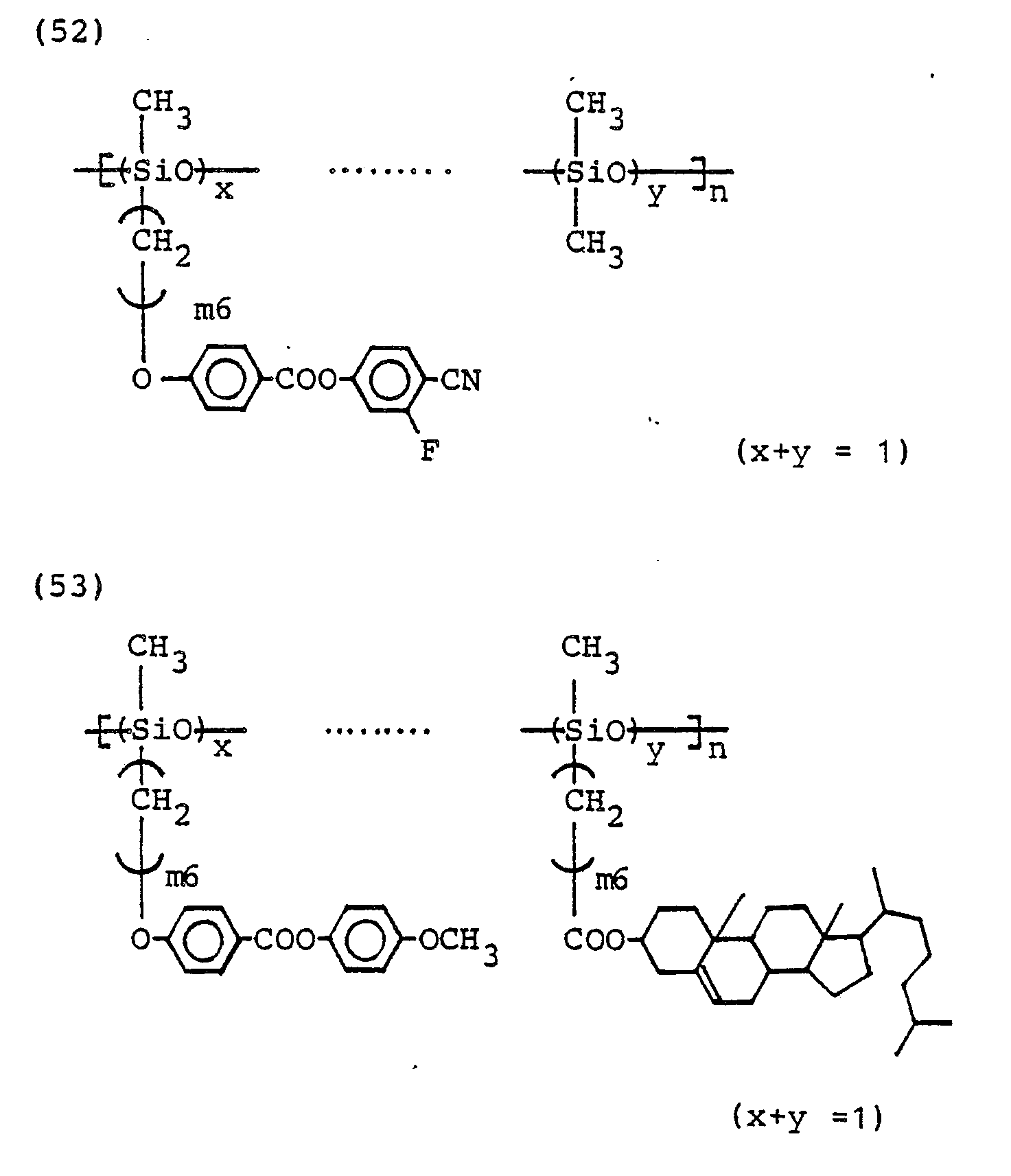
- The polymer liquid crystal may preferably have 5 to 1000 recurring units therein. Examples of the polymer liquid crystal used in the present invention may include those represented by the following formulas (1) - (60).
- In the formulas (1) - (13) below, 1 ≦ n < 15, and p = 5 - 1000.


- In the formulas (14) - (60) below, p = 5 - 1000, p1+p2 = 5 - 1000, q = 1 - 16, q1 = 1 -16 and q2 = 1 - 16.


- In the formulas (18) - (46) below, * denotes the location of an asymmetric carbonatom, and n = 5 - 1000.


- In the formulas (52) - (60), m6 = 1 - 18, and n = 5 - 1000.


- For such a polymer liquid crystal as described above, it is important to have a flexible chain structure in order to form a good helical structure in chiral smectic C phase. Such a flexible chain may be alkyl chain, an alkylene chain, a poly(alkyloxy) chain, an acryl chain or a methacryl chain, and may preferably be one having a large degree of freedom and flexibility. A particularly preferred class of polymer liquid crystals may be those having a poly(dimethylsiloxane) unit as a flexible chain.
- A polymer liquid crystal may have an optically active group which may for example be 2-methylbutyl group, 1-methylpropyl group, 1-methyl-heptyl group or cholesterol group. A polymer liquid crystal having a structure of a large steric hindrance is liable to provide a small helical pitch.
- In case where a polymer liquid crystal per se has no optically active group, it is necessary to mix the polymer liquid crystal with a compound having an optically active group, which may preferably be a low-molecular weight ferroelectric liquid crystal. Examples of the low-molecular weight ferroelectric liquid crystal may include those represented by the following formulas (1) - (15) together with phase transition characteristics. Herein, the respective symbols denote the following phases:
Cryst.: crystal, SmC*: chiral smectic C phase, SmH*: chiral smectic H phase, SmA: smectic A phase, SmB: smectic B phase, Sm3: un-identified smectic phase, Ch.: cholesteric phase, N: nematic phase, and Iso.: isotropic phase. 


- In such a liquid crystal composition comprising a polymer liquid crystal having an asymmetric carbon atom and a low molecular weight liquid crystal, it is preferred that the polymer liquid crystal is contained in a proportion of 30 wt. % or more, particularly 50 wt. % or more. Below 30 wt. %, it is difficult to effect sufficient fixation of the helical structure.
- Such a polymer liquid crystal or a polymer liquid crystal composition obtained from such a polymer liquid crystal may be used in a separate film or may be formed in a layer disposed on a substrate. The polymer liquid crystal layer may have a thickness of 1 - 200 microns, preferably 5 - 100 microns.
- In case where writing or erasure is effected by using laser light etc., an improved sensitivity can be obtained by disposing a laser light-absorbing layer or adding a laser light absorbing compound into the polymer liquid crystal layer. Examples of such a laser light-absorbing compound to be added into the polymer liquid crystal layer may include those represented by the following formulas.


- Further, it is possible to add an ultraviolet absorber, a deterioration preventing agent such as an anti-oxidant, a nucleating agent or a fluorescent dye.
- It is preferred to subject a polymer liquid crystal layer thus obtained to orientation or aligning treatment, but the recording medium of the present invention provides a high contrast without complete orientation. In order to realize a helical structure and a non-helical structure by using a response to an electric field in the chiral smectic C phase, it is particularly effective to use an alignment film.
- The orientation or aligning treatment may be a homogeneous aligning treatment or a homeotropic aligning treatment. The homogeneous aligning treatment may be performed by stretching under the action of a mechanical force, roller stretching, shearing, application of an electric field or magnetic field or interfacial control. In case where a substrate is used, a homogeneous aligning treatment by interfacial control is particularly preferred.
- Specific examples of the homogeneous aligning treatment by interfacial control may include the following.
- A substrate is coated with an alignment control film by forming a film of e.g. an inorganic insulating substance, such as silicon monoxide, silicon dioxide, aluminum oxide, zirconia, magnesium fluoride, cerium oxide, cerium fluoride, silicon nitride, silicon carbide or boron nitride; or an organic insulating substance, such as polyvinyl alcohol, polyimide, polyamideimide, polyesterimide, polyparaxylylene, polyester, polycarbonate, polyvinylacetal, polyvinylchloride, polyamide, polystyrene, cellulosic resin, melamine resin, urea resin or acrylic resin, by application of a solution, vapor deposition or sputtering.
- The alignment control film formed as a film of an inorganic insulating substance or organic insulating substance as described above may then be rubbed in one direction with velvet, cloth or paper on the surface thereof.
- An oxide such as SiO, a fluoride, or a metal such as Au or Al or its oxide, is vapor-deposited on a substrate in a direction forming an angle inclined with respect to the substrate.
- An organic or inorganic insulating film as described in (1) above formed on a substrate is etched by radiation with an ion beam or oxygen plasma incident in an oblique direction.
- A film of obtained by stretching a film of a polymer such as polyester or polyvinyl alcohol also shows a good orientation characteristic.
- Grooves are formed on a substrate surface by photolithography, stamping or injection.
- The homeotropic aligning treatment may be performed by stretching under the action of a mechanical force, roller stretching, shearing, application of an electric field or magnetic field, or interfacial control. In case where a substrate is used, a homeotropic aligning treatment by interfacial control is particularly referred.
- Specific examples of the homeotropic aligning treatment by interfacial control may include the following.
- A substrate surface is coated with a layer of an organic silane, lecithin or PTFE (polytetrafluoroethylene) having a homeotropic orientation characteristic.
- Oblique vapor deposition is performed on a substrate while the substrate is rotated and the vapor deposition angle is appropriately selected to provide a homeotropic orientation characteristic. Further, it is also possible to apply a homeotropic aligning agent as shown in (1) above after the oblique vapor deposition.
- Various orientation or aligning treatments as described above may be used singly or in combination of two or more methods.
- In the present invention, a helical structure in chiral smectic C phase is used as a recorded state. As a result, when a reflected light quantity for a specific wavelength of light is measured, it has been found that the reflected light quantity continuously changes depending on the change in helical pitch. Therefore, if the polymer liquid crystal layer is held at a controlled temperature to select a helical pitch and then cooled to fix the helical pitch as a recorded state, a continuous change in reflected light quantity can be obtained and is effectively used for multi-value recording.
- On the other hand, the proportion of such a helical structure can be controlled by interfacial effect or external field, and is similarly used for multi-value recording. Therefore, gradational display can be effected relatively easily.
- Figures 3 and 4 respectively illustrate the laminar structure of an embodiment of the recording medium constituted as described above and operation thereof according to the present invention, and Figures 1 and 6 respectively illustrate an embodiment of the optical modulation device incorporating such a recording medium according to the present invention. In these figures, like parts are denoted by the same reference numerals.
- More specifically, referring to Figure 3, a recording medium comprises in a successively laminated form a substrate 1, a
transparent electrode 2, analignment film 3, a polymerliquid crystal layer 4, a reflection layer andlower electrode 5, and a substrate 1a. A recording medium shown in Figure 4 comprises in a successively laminated form a substrate 1, alower electrode 30, a polymerliquid crystal layer 4 and aprotective layer 18, and is used in combination with a thermal head 6 for recording. - Figure 1 shows an optical modulation apparatus incorporating the recording medium shown in Figure 3 and further comprising a
laser source 7, acollimator lens 8, anoptical modulator 9 connected to amodulation signal generator 10, a polarized beam splitter 11, aquarter wave plate 12, acondenser lens 13 connected to anactuator 14, avoltage modulator 15, amedium driver 16, and adetector 17. - Figure 5 shows another optical modulation apparatus incorporating a recording medium or display medium 19 in the form of an endless belt and further comprising a drive and
heating roller 20, aplanar heater 21, asemiconductor laser 22, apolygonal mirror 23, an f-ϑ lens 24, atransparent electrode 25, alower electrode 26,illumination light sources 27, ablack body 28 and aninside face mirror 29. - Further, when a display layer comprising a polymer liquid crystal layer having a principal axis of helical structure disposed substantially perpendicularly to the display layer is used, the degree of selective scattering is enhanced to provide a display with improved contrast and color purity.
- More specifically, such a display layer comprising a polymer liquid crystal having its principal axis of helical structure disposed substantially perpendicularly to the display layer is selectively heated to a prescribed temperature above the glass transition point of the polymer liquid crystal to provide a selectively varied helical pitch and then cooled below the glass transition point to fix the selective scattering wavelength of the polymer liquid crystal.
- In order to provide a display layer comprising a polymer liquid crystal having its principal axis of helical structure disposed substantially perpendicularly to the display layer in the display medium of the present invention, it is preferred to effect an aligning treatment for the polymer liquid crystal. For example, when a polymer liquid crystal having a helical structure is used for display in its chiral smectic phase, it is preferred to effect the above-mentioned homeotropic aligning treatment. On the other hand, when a polymer liquid crystal is used in its chiral nematic phase for display, it is preferred to effect the above-mentioned homogeneous aligning treatment.
- This embodiment will be explained in more detail with reference to drawings.
- Figure 6 is an illustration of such a display medium of the present invention and an embodiment of the display method using the medium. Referring to Figure 6, a display medium comprises a
substrate 31 and a light-absorbinglayer 32 and analignment control film 33 disposed successively on thesubstrate 31. On thealignment control film 33 is disposed adisplay layer 34 comprising a polymerliquid crystal compound 35 having a helical structure. The principal axis of the helical structure is disposed substantially perpendicularly to thedisplay layer 34 and such a helical structure is structurally fixed below the glass transition point of the polymer liquid crystal. Thedisplay layer 34 is further coated with aprotective layer 36. - In display operation, such a display medium having a
display layer 34 comprising a polymerliquid crystal compound 35 having a helical structure with its principal axis being disposed substantially perpendicularly to thedisplay layer 34 is subjected to selective heating with athermal head 38 controlled by adrive pulse modulation 39 to selectively heatdisplay layer 34 to a prescribed temperature above the glass transition point of thepolymer liquid crystal 35, thereby providing a selected helical pitch. In this way, the helical pitch is selectively changed, so that a highly fine color image can be repetitively displaced and erased. - Figure 7 is an illustration of another embodiment of the display medium and display method using the medium of the present invention. Referring to Figure 7, the display medium comprises a
substrate 31 and successively thereon an alignment control film and light absorbinglayer 37, and adisplay layer 34 comprising a polymerliquid crystal compound 35 having a helical structure. - In displaying operation using the display medium, the display medium is irradiated with a laser light issued from a
laser source 43 under the control of alaser modulator 42 and passed through apolygonal scanner 41 and an f-ϑ lens 40 to selectively heat thedisplay layer 34 to a prescribed temperature above the glass transition point of thepolymer liquid crystal 35 and select a pitch of the helical structure, and then cooled substantially below the glass transition point to determine a selective scattering wavelength of the polymer liquid crystal and change the helical pitch, so that a highly fine color image can be repetitively displayed and erased. - In the display medium of the present invention subjected to an aligning treatment as described in the above manner, the principal axis of helical structure of the polymer liquid crystal constituting the display layer is disposed substantially perpendicularly to the display layer, so that selective scattering can be effected very effectively. Conventionally, when a helical pitch is fixed in a glass state, a color purity has become poor because of an increase in half-width value of the selective scattering. This problem has been alleviated by the present invention. Further, a color change due to a change in view angle is also alleviated.
- The wavelength causing selective scattering depends on a helical pitch and is represented by the formula of λ = np, wherein n denotes a refractive index p denotes a helical pitch and λ denotes the wavelength of selective scattering. Color display can be effected by changing the helical pitch. In the present invention, the helical pitch may desirably be set within a range of ordinarily 250 - 800 nm, preferably 400 - 700 nm. Below 250 nm, a sufficient selective scattering efficiency is not attained, and above 800 nm, writing laser light may also be scattered.
- In a change in helical pitch within the above-described range may for example be effected by temperature change, copolymerization, or electric field response and respectively can be used for color display.
- The selective scattering effect obtained by the control of helical pitch in the above-described manner can be stably fixed by cooling the recording layer comprising a polymer liquid crystal to below the glass transition point. This is because the helical pitch is fixed below the glass transition point. Thus, a good image is retained as it is, so that repetitive writing is not required and the writing energy is minimized.
- It is possible to provide a surface protective layer on the optical modulation medium, i.e., recording medium or display medium of the present invention. It is preferred that the protective layer is free from thermal deterioration or thermal deformation when a thermal head etc. is used for writing and erasure.
- Further, it is also possible to provide a light-absorbing layer to absorb a portion of light other than selectively scattered light and improve the contrast.
- In the optical modulation medium of the present invention, in order to control the temperature of the optical modulation layer comprising a polymer liquid crystal above the glass transition point for writing and erasure, laser light or a thermal head may be used. In writing, the display layer is raised to a temperature causing a change in helical structure of the polymer liquid crystal by irradiation with laser light or thermal pulse application by a thermal head and then rapidly cooled to provide an optical density different from that before the writing.
- A polymer liquid crystal having a helical structure assumes chiral nematic phase or chiral smectic phase. Accordingly, it is preferred that the polymer liquid crystal has its chiral phase temperature range in the range of 0 to 300 oC. Below 0 oC, temperature control is difficult. Above 300 oC is not preferred because of excessive energy consumption. A further preferred chiral phase temperature range is 20 to 250 oC.
- Erasure may be effected by holding the optical modulation layer at a prescribed temperature above the glass transition point of the polymer liquid crystal.
- Writing in the optical modulation medium comprising a polymer liquid crystal may be effected more specifically as follows.
- (1) A display layer comprising a polymer liquid crystal is subjected to heat application to change the helical pitch and select a display color under temperature control. Then, the medium is cooled to hold the display color and density. Gradational display may be performed by controlling the liquid crystal proportion.
- (2) Polymer liquid crystals having different helical pitches are respectively applied in the form of stripes or mosaic to form a display layer. The respective polymer liquid crystal parts are addressed and heated to prescribed temperatures by heat application means to control the display colors and densities.
- (3) A display layer comprising a polymer liquid crystal is disposed between electrodes and heated above the glass transition point under application of an electric field to change the helical pitch.
- By controlling the time and temperature for the heat treatment in the above-described display methods, it is possible to control not only the wavelength of selective scattering but also the quantity of scattering at a prescribed selective scattering wavelength, whereby a gradational display or full-color display can be performed.
- In order to perform erasure for example by removal of the helical structure, a display layer is heated into, for example, an isotropic phase and then rapidly cooled to form a transparent state, or supplied with an electric field to form a transparent state.
- Hereinafter, the present invention will be explained by way of examples.
- A recording medium as shown in Figure 3 was prepared in the following manner. A polyamic acid solution was applied by spin coating on a glass substrate 1 having a
transparent electrode 2 and heat cured at 300 oC to form apolyimide alignment film 3. Separately, a polymer liquid crystal composition was prepared by mixing the following polymer liquid crystals (I) and (II) in a weight ratio of 2:1 and adding thereto 0.5 wt. % of a dye represented by the following formula (III).
SmC*: chiral smectic phase Ch.: cholesteric phase Iso.: isotropic phase 
- The above prepared polymer liquid crystal composition was sandwiched between the above treated glass substrate 1 and a glass substrate 1a having thereon a 5000 Å-thick reflection layer and
lower electrode 5 and heat-bonded at 150 oC under vacuum. An about 50 micron-thick polymerliquid crystal layer 4 was formed in the thus prepared recording medium. Then, the medium was gradually cooled from 120 oC and observed through a reflection-type polarizing microscope, wherein a periodical helical structure was observed at 60 oC (SmC*). - An optical modulation system as shown in Figure 1 was prepared by using the recording medium prepared in Example 1.
- Laser light issued from a
laser source 7 was modulated by anoptical modulator 9 with signals from amodulation signal generator 10 and passed through a polarized light beam splitter 11 to be converted into linearly polarized light. The linearly polarized light was passed through aquarter wave plate 12 to form a circularly polarized light, which was then passed through acondenser lens 13 to be incident on the recording medium prepared in Example 1. - Figure 3 is a enlarged view of the recording medium irradiated with the laser light. The laser power was 2 mW on the medium. The reflectance was about 20 %. Then, the polarized beam splitter 11 was rotated by 90 degrees to provide a 90 degree-rotated linear polarized light, which was then similarly passed through the
quarter wave plate 12 to be converted into circularly polarized light of reverse rotation. The circularly polarized light was similarly passed through thecondenser lens 13 to be incident on the medium, whereby the reflectance was increased to 35 %. - Then, a DC voltage of 100 V was applied to the recording medium by a
voltage modulator 15 to completely remove the helical structure, whereby the reflectance was increased to 50 % in about 200 msec. The laser light was stopped and again incident on the medium at a laser power of 0.5 mW, whereby no change in reflectance was observed. - A display apparatus as shown in Figure 5 was prepared.
- A substrate of a PET film coated with an ITO transparent electrode by sputtering was further coated by a roller coater with the polymer liquid crystal composition prepared in Example 1 heated at 120 oC. The surface was further coated with a 5 micron-thick polyamide film under pressure and both ends of the laminate film thus obtained was bonded to each other to form a
display medium 19 in the form of an endless film. The display medium was rotated by adrive roller 20 and held at 80 oC by aplanar heater 21 to form a helical structure. The display medium was then irradiated with modulated laser light at a power of 20 mW from asemiconductor laser 22 to be sufficiently heated into an isotropic phase and then rapidly cooled to form a recorded part of a non-helical structure. During the recording, the laser light was deflected by apolygonal mirror 23 for scanning in one direction and passed through an f-ϑ lens 24 to be focused on the medium 19, whereby a good contrast of image was obtained. - A recording and reproduction system using a thermal head as shown in Figure 4 was prepared.
- A 2:1 mixture of polymer liquid crystal compounds (1) and (2) used in Example 1 was applied on a glass substrate 1 coated with an ITO
transparent electrode 30 in a thickness of about 30 microns and gradually cooled from 120 oC to form a polymer liquid crystal layer. Further thereon, an ultraviolet-curable type fluorine-containing resin was applied in a thickness of 2 microns and irradiated with ultraviolet rays for curing to form aprotective layer 18, thus forming a four-layer structured recording medium. The medium was caused to contact an energized thermal head 6 and a bias voltage of 200 V was applied between thelower electrode 30 and the thermal head 6. Then a recorded portion of a non-helical structure was formed by cutting the current for cooling, whereby a display with a contrast of 2:1 was obtained. Further, when the medium was sandwiched between two polarizers, a display at a contrast of 10:1 was obtained and stably retained at room temperature. - A 0.8 mm-thick glass substrate was coated with a 500 Å-thick polyimide film by application and heat-curing. Polyimide film was subjected to a uniaxial aligning treatment and coated by dipping with a solution of a polymer liquid crystal represented by the following structural formula (IV) in dichloroethane to form a display layer.

- After drying, a uniaxially rubbing treated polyimide film was disposed on the display layer, and the laminate was heated into an isotropic phase, gradually cooled and held at about 130 oC for 90 min. to form a homogeneously orientation-treated cholesteric phase. The display layer thus treated was found to have a thickness of about 10 microns.
- The thus prepared display medium showed a selective scattering at around 600 nm and was observed in red. The display medium was observed through a polarizing microscope and found to be uniform and non-anisotropic. The center axis of helical structure in cholesteric phase was found to be perpendicular to the display layer. Then, the display layer was caused to contact a thermal head and supplied with a heat pulse to be heated to above 200 oC, whereby the heated portion became transparent to provide a good contrast, which was stably retained at room temperature for more than 1 week.
- The erasure was effected by holding the medium at about 130 oC for 90 min. to form cholesteric phase again.
- A dichloroethane solution of a polymer liquid crystal represented by the following structural formula (V) was applied by screen printing. After drying, the polymer liquid crystal layer was heated to 200 oC and gradually cooled to form a homogeneous orientation-treated uniform cholesteric phase. The display layer showed a thickness of about 50 microns. As a result of observation through a polarizing microscope, a uniform and non-anisotropic cholesteric phase was found to be formed, and the helical center axis was found to be perpendicular to the display layer.
- The thus prepared display medium was irradiated with semiconductor laser light (wavelength: 830 nm), whereby the irradiated portion was written in a colorless state.

- Erasure was performed by irradiating a specified part with laser light at 10 mW for 1 sec.
- A 0.8 mm-thick glass substrate was coated with a methanol solution of a silane coupling agent (SH6040, available from Toray Silicone K.K.), which was then heat-cured to form a homeotropic alignment film. The substrate was further coated by spin coating with a dichloroethane solution of a polymer liquid crystal represented by the following structural formula (VI).

- After drying, the polymer liquid crystal layer was heated to 250 oC and gradually cooled to form a homeotropically orientation-treated SmC* phase. The display layer showed a thickness of about 20 microns. As a result of observation through a polarizing microscope, the display layer was found to be uniform and non-anisotropic. A helical central axis in SmC* phase was found to be perpendicular to the display layer.
- The thus prepared display medium was subjected to heat application by a thermal head, whereby a good contrast was obtained.
- Erasure was performed by holding the display layer at about 180 oC for 2 sec. similarly by a thermal head. The medium was further irradiated with circularly polarized light obtained by passing laser light of 1 mW and 830 nm through a polarized beam splitter and a quarter wave plate to measure the reflected light quantity, whereby the reflectance from the portion recorded by the thermal head was 5 % and the reflectance from the non-recorded portion was 40 %, thus showing a high S/N ratio.
- As described hereinabove, according to the present invention, there is provided a recording medium having an optical modulation layer comprising a polymer liquid crystal layer having a helical structure in chiral smectic C phase. When the recording medium is applied to an optical modulation system for controlling the helical structure and the non-helical structure, there is provided an optical modulation apparatus capable of providing images of a large area, a high degree of fineness and a high contrast and also showing large recording and erasure speeds at a low cost.
- The present invention further provides a display medium having a display layer comprising a polymer liquid crystal forming a helical structure with its central axis disposed perpendicularly to the display layer. The display medium provides a highly fine color image without a display-holding operation. The display medium further provides a display showing a high selective scattering efficiency, a good contrast and a good color purity.
- An optical modulation device is provided by forming an optical modulation layer comprising a polymer liquid crystal having a helical structure and a non-helical structure in chrial smectic C phase. The helical structure of the polymer liquid crystal is selectively formed or removed to provide a recorded state. The recorded state is held below the glass transition point of the polymer liquid crystal. The helical pitch of the helical structure can be selectively changed to form a recorded state. The helical structure can be formed to dispose its principal axis perpendicularly to the polymer liquid crystal layer. The recorded state may be read out by detecting a reflectance from the polymer liquid crystal layer.
Claims (11)
providing a recording medium having a layer of a polymer liquid crystal having chiral smectic C phase, and selectively causing a helical structure or a non-helical structure in the chiral smectic C phase to form a recorded state comprising a combination of a helical structure and a non-helical structure in the polymer liquid crystal layer.
providing a recording medium having a layer of a polymer liquid crystal having chiral smectic C phase, and forming a helical structure in the chiral smectic C phase in the polymer liquid crystal layer to form a recorded state comprising a combination of different helical pitches in the helical structure.
Applications Claiming Priority (4)
| Application Number | Priority Date | Filing Date | Title |
|---|---|---|---|
| JP63115774A JP2632920B2 (en) | 1988-05-11 | 1988-05-11 | Recording method, recording medium and recording device |
| JP115774/88 | 1988-05-11 | ||
| JP134422/88 | 1988-06-02 | ||
| JP13442288A JPH01304431A (en) | 1988-06-02 | 1988-06-02 | Display medium and display method thereof |
Publications (3)
| Publication Number | Publication Date |
|---|---|
| EP0349731A2 true EP0349731A2 (en) | 1990-01-10 |
| EP0349731A3 EP0349731A3 (en) | 1991-01-02 |
| EP0349731B1 EP0349731B1 (en) | 1996-03-27 |
Family
ID=31718857
Family Applications (1)
| Application Number | Title | Priority Date | Filing Date |
|---|---|---|---|
| EP89108441A Expired - Lifetime EP0349731B1 (en) | 1988-05-11 | 1989-05-10 | Optical modulation device using polymer liquid crystal |
Country Status (3)
| Country | Link |
|---|---|
| US (1) | US5272552A (en) |
| EP (1) | EP0349731B1 (en) |
| DE (1) | DE68926071T2 (en) |
Cited By (2)
| Publication number | Priority date | Publication date | Assignee | Title |
|---|---|---|---|---|
| EP0450952A3 (en) * | 1990-04-04 | 1992-06-03 | Victor Company Of Japan, Ltd. | Optical system for a colour picture display |
| EP0474473A3 (en) * | 1990-09-07 | 1992-08-05 | Gec-Marconi Limited | Optical storage devices |
Families Citing this family (7)
| Publication number | Priority date | Publication date | Assignee | Title |
|---|---|---|---|---|
| JP2851906B2 (en) * | 1990-03-23 | 1999-01-27 | キヤノン株式会社 | Optical modulation element and display device |
| US5625477A (en) * | 1994-04-11 | 1997-04-29 | Advanced Display Systems, Inc. | Zero field multistable cholesteric liquid crystal displays |
| US5889566A (en) * | 1994-04-11 | 1999-03-30 | Advanced Display Systems, Inc. | Multistable cholesteric liquid crystal devices driven by width-dependent voltage pulse |
| EP0982605A1 (en) * | 1998-08-26 | 2000-03-01 | MERCK PATENT GmbH | Reflective film |
| JP4107767B2 (en) * | 1999-06-23 | 2008-06-25 | ソニー株式会社 | Optical recording medium, recording / reproducing method and recording / reproducing apparatus using the same |
| US7286111B2 (en) * | 2003-11-13 | 2007-10-23 | Eastman Kodak Company | Apparatus for electro-optically writing a display |
| TWI348408B (en) * | 2004-04-28 | 2011-09-11 | Olympus Corp | Laser processing device |
Family Cites Families (11)
| Publication number | Priority date | Publication date | Assignee | Title |
|---|---|---|---|---|
| DE2831909A1 (en) * | 1978-07-20 | 1980-02-07 | Basf Ag | LIQUID CRYSTALLINE POLYMER PHASE WITH CHOLESTERIC STRUCTURE, METHOD FOR THE PRODUCTION THEREOF AND THEIR USE |
| GB8324642D0 (en) * | 1983-09-14 | 1983-10-19 | Univ Manchester | Liquid crystal storage device |
| FR2581209B1 (en) * | 1985-04-26 | 1993-11-05 | Canon Kk | LIQUID CRYSTAL OPTICAL DEVICE |
| US4844835A (en) * | 1985-12-26 | 1989-07-04 | Idenitsu Kosan Co., Ltd. | Ferroelectric liquid crystal polymer |
| JPS62175939A (en) * | 1986-01-29 | 1987-08-01 | Nippon Oil Co Ltd | Recording medium |
| GB8616165D0 (en) * | 1986-07-02 | 1986-08-06 | Stc Plc | Liquid crystal cell |
| US5029983A (en) * | 1986-12-06 | 1991-07-09 | Semiconductor Energy Laboratory Co., Ltd. | Liquid crystal device with a smectic chiral liquid crystal |
| EP0271900B1 (en) * | 1986-12-17 | 1993-12-29 | Canon Kabushiki Kaisha | Device, method and apparatus for optical modulation |
| EP0296571B1 (en) * | 1987-06-22 | 1994-03-30 | Idemitsu Kosan Company Limited | Method of producing a liquid crystal optical element |
| US5066107A (en) * | 1988-06-16 | 1991-11-19 | Canon Kabushiki Kaisha | Liquid crystal display medium, liquid crystal display method and liquid crystal display apparatus for outputting color images |
| JP2741540B2 (en) * | 1989-07-10 | 1998-04-22 | キヤノン株式会社 | Color image forming equipment |
-
1989
- 1989-05-05 US US07/347,920 patent/US5272552A/en not_active Expired - Fee Related
- 1989-05-10 EP EP89108441A patent/EP0349731B1/en not_active Expired - Lifetime
- 1989-05-10 DE DE68926071T patent/DE68926071T2/en not_active Expired - Fee Related
Cited By (2)
| Publication number | Priority date | Publication date | Assignee | Title |
|---|---|---|---|---|
| EP0450952A3 (en) * | 1990-04-04 | 1992-06-03 | Victor Company Of Japan, Ltd. | Optical system for a colour picture display |
| EP0474473A3 (en) * | 1990-09-07 | 1992-08-05 | Gec-Marconi Limited | Optical storage devices |
Also Published As
| Publication number | Publication date |
|---|---|
| EP0349731B1 (en) | 1996-03-27 |
| EP0349731A3 (en) | 1991-01-02 |
| DE68926071D1 (en) | 1996-05-02 |
| DE68926071T2 (en) | 1996-11-14 |
| US5272552A (en) | 1993-12-21 |
Similar Documents
| Publication | Publication Date | Title |
|---|---|---|
| EP0271900B1 (en) | Device, method and apparatus for optical modulation | |
| EP0306925B1 (en) | Recording method and recording apparatus | |
| US5444651A (en) | Non-volatile memory device | |
| EP0819305B1 (en) | Liquid crystal optical storage medium with gray scale | |
| US4405993A (en) | Liquid crystal disc memory system | |
| EP0346911B1 (en) | Display medium, display method and display apparatus | |
| EP1063645B1 (en) | Optical recording medium | |
| US5353247A (en) | Optical mass storage system and memory cell incorporated therein | |
| WO1983001841A1 (en) | Liquid crystal display unit | |
| EP0349731B1 (en) | Optical modulation device using polymer liquid crystal | |
| EP0461619B1 (en) | Information memory medium and information recording/holding process making use of the medium | |
| JPS62231437A (en) | Optical recording medium and optical recording method | |
| Shibaev | Electrooptical and photooptical properties of polymer liquid crystals | |
| JP3141299B2 (en) | Recording method and recording device | |
| EP0540153B1 (en) | A non-volatile memory device | |
| GB2248963A (en) | Compact discs | |
| EP1428167A2 (en) | Multilayer combined liquid crystal optical memory systems with means for recording and reading information | |
| Birecki et al. | Erasable Optical Liquid Crystal Disc Memory | |
| JP2632920B2 (en) | Recording method, recording medium and recording device | |
| KR940006131B1 (en) | Reversible Optical Information Storage Method Using Liquid Crystal Polymer as Information Recording Medium | |
| US5486311A (en) | Optically erasable read-and-write liquid crystal/side-chain liquid crystalline polymer composition and method of making recordation on the same | |
| JP2703913B2 (en) | Recording / reproducing apparatus and recording / reproducing method | |
| JP3030425B2 (en) | Recording method and recording device | |
| JPH07161039A (en) | Recording / reproducing method for optical recording medium | |
| JPH02284130A (en) | Information memory medium and information memory device |
Legal Events
| Date | Code | Title | Description |
|---|---|---|---|
| PUAI | Public reference made under article 153(3) epc to a published international application that has entered the european phase |
Free format text: ORIGINAL CODE: 0009012 |
|
| 17P | Request for examination filed |
Effective date: 19890510 |
|
| AK | Designated contracting states |
Kind code of ref document: A2 Designated state(s): DE FR GB IT |
|
| PUAL | Search report despatched |
Free format text: ORIGINAL CODE: 0009013 |
|
| AK | Designated contracting states |
Kind code of ref document: A3 Designated state(s): DE FR GB IT |
|
| 17Q | First examination report despatched |
Effective date: 19930624 |
|
| GRAA | (expected) grant |
Free format text: ORIGINAL CODE: 0009210 |
|
| AK | Designated contracting states |
Kind code of ref document: B1 Designated state(s): DE FR GB IT |
|
| PG25 | Lapsed in a contracting state [announced via postgrant information from national office to epo] |
Ref country code: IT Free format text: LAPSE BECAUSE OF FAILURE TO SUBMIT A TRANSLATION OF THE DESCRIPTION OR TO PAY THE FEE WITHIN THE PRESCRIBED TIME-LIMIT;WARNING: LAPSES OF ITALIAN PATENTS WITH EFFECTIVE DATE BEFORE 2007 MAY HAVE OCCURRED AT ANY TIME BEFORE 2007. THE CORRECT EFFECTIVE DATE MAY BE DIFFERENT FROM THE ONE RECORDED. Effective date: 19960327 Ref country code: FR Effective date: 19960327 |
|
| REF | Corresponds to: |
Ref document number: 68926071 Country of ref document: DE Date of ref document: 19960502 |
|
| GRAH | Despatch of communication of intention to grant a patent |
Free format text: ORIGINAL CODE: EPIDOS IGRA |
|
| EN | Fr: translation not filed | ||
| PLBE | No opposition filed within time limit |
Free format text: ORIGINAL CODE: 0009261 |
|
| STAA | Information on the status of an ep patent application or granted ep patent |
Free format text: STATUS: NO OPPOSITION FILED WITHIN TIME LIMIT |
|
| 26N | No opposition filed | ||
| REG | Reference to a national code |
Ref country code: GB Ref legal event code: IF02 |
|
| PGFP | Annual fee paid to national office [announced via postgrant information from national office to epo] |
Ref country code: GB Payment date: 20040505 Year of fee payment: 16 |
|
| PGFP | Annual fee paid to national office [announced via postgrant information from national office to epo] |
Ref country code: DE Payment date: 20040520 Year of fee payment: 16 |
|
| PG25 | Lapsed in a contracting state [announced via postgrant information from national office to epo] |
Ref country code: GB Free format text: LAPSE BECAUSE OF NON-PAYMENT OF DUE FEES Effective date: 20050510 |
|
| PG25 | Lapsed in a contracting state [announced via postgrant information from national office to epo] |
Ref country code: DE Free format text: LAPSE BECAUSE OF NON-PAYMENT OF DUE FEES Effective date: 20051201 |
|
| GBPC | Gb: european patent ceased through non-payment of renewal fee |
Effective date: 20050510 |