EP0349715A2 - Procédé et circuit pour produire un signal d'horloge décalé en phase - Google Patents
Procédé et circuit pour produire un signal d'horloge décalé en phase Download PDFInfo
- Publication number
- EP0349715A2 EP0349715A2 EP89106224A EP89106224A EP0349715A2 EP 0349715 A2 EP0349715 A2 EP 0349715A2 EP 89106224 A EP89106224 A EP 89106224A EP 89106224 A EP89106224 A EP 89106224A EP 0349715 A2 EP0349715 A2 EP 0349715A2
- Authority
- EP
- European Patent Office
- Prior art keywords
- phase
- signal
- frequency
- shifted
- output
- Prior art date
- Legal status (The legal status is an assumption and is not a legal conclusion. Google has not performed a legal analysis and makes no representation as to the accuracy of the status listed.)
- Granted
Links
- 238000000034 method Methods 0.000 title claims abstract description 10
- 230000010363 phase shift Effects 0.000 claims description 22
- 230000003111 delayed effect Effects 0.000 claims 4
- 230000002238 attenuated effect Effects 0.000 claims 3
- 230000005540 biological transmission Effects 0.000 abstract 1
- 230000003287 optical effect Effects 0.000 abstract 1
- 238000010586 diagram Methods 0.000 description 5
- 230000000694 effects Effects 0.000 description 4
- 239000003990 capacitor Substances 0.000 description 2
- 230000003071 parasitic effect Effects 0.000 description 2
- 230000008929 regeneration Effects 0.000 description 2
- 238000011069 regeneration method Methods 0.000 description 2
- 230000002411 adverse Effects 0.000 description 1
- 238000009826 distribution Methods 0.000 description 1
- 239000000835 fiber Substances 0.000 description 1
- 230000000717 retained effect Effects 0.000 description 1
- 239000000758 substrate Substances 0.000 description 1
- 230000007704 transition Effects 0.000 description 1
Images


Classifications
-
- H—ELECTRICITY
- H04—ELECTRIC COMMUNICATION TECHNIQUE
- H04J—MULTIPLEX COMMUNICATION
- H04J3/00—Time-division multiplex systems
- H04J3/02—Details
- H04J3/04—Distributors combined with modulators or demodulators
- H04J3/047—Distributors with transistors or integrated circuits
-
- H—ELECTRICITY
- H03—ELECTRONIC CIRCUITRY
- H03K—PULSE TECHNIQUE
- H03K5/00—Manipulating of pulses not covered by one of the other main groups of this subclass
- H03K5/13—Arrangements having a single output and transforming input signals into pulses delivered at desired time intervals
-
- H—ELECTRICITY
- H03—ELECTRONIC CIRCUITRY
- H03K—PULSE TECHNIQUE
- H03K5/00—Manipulating of pulses not covered by one of the other main groups of this subclass
- H03K5/13—Arrangements having a single output and transforming input signals into pulses delivered at desired time intervals
- H03K5/135—Arrangements having a single output and transforming input signals into pulses delivered at desired time intervals by the use of time reference signals, e.g. clock signals
-
- H—ELECTRICITY
- H03—ELECTRONIC CIRCUITRY
- H03K—PULSE TECHNIQUE
- H03K5/00—Manipulating of pulses not covered by one of the other main groups of this subclass
- H03K2005/00013—Delay, i.e. output pulse is delayed after input pulse and pulse length of output pulse is dependent on pulse length of input pulse
- H03K2005/0015—Layout of the delay element
- H03K2005/00163—Layout of the delay element using bipolar transistors
- H03K2005/00176—Layout of the delay element using bipolar transistors using differential stages
-
- H—ELECTRICITY
- H03—ELECTRONIC CIRCUITRY
- H03K—PULSE TECHNIQUE
- H03K5/00—Manipulating of pulses not covered by one of the other main groups of this subclass
- H03K2005/00013—Delay, i.e. output pulse is delayed after input pulse and pulse length of output pulse is dependent on pulse length of input pulse
- H03K2005/0015—Layout of the delay element
- H03K2005/00163—Layout of the delay element using bipolar transistors
- H03K2005/00182—Layout of the delay element using bipolar transistors using constant current sources
-
- H—ELECTRICITY
- H03—ELECTRONIC CIRCUITRY
- H03K—PULSE TECHNIQUE
- H03K5/00—Manipulating of pulses not covered by one of the other main groups of this subclass
- H03K2005/00013—Delay, i.e. output pulse is delayed after input pulse and pulse length of output pulse is dependent on pulse length of input pulse
- H03K2005/0015—Layout of the delay element
- H03K2005/00228—Layout of the delay element having complementary input and output signals
-
- H—ELECTRICITY
- H04—ELECTRIC COMMUNICATION TECHNIQUE
- H04J—MULTIPLEX COMMUNICATION
- H04J3/00—Time-division multiplex systems
- H04J3/02—Details
- H04J3/06—Synchronising arrangements
- H04J3/0635—Clock or time synchronisation in a network
- H04J3/0685—Clock or time synchronisation in a node; Intranode synchronisation
Definitions
- the invention relates to a method for generating a phase-shifted clock signal according to the preamble of claim 1 or to a circuit arrangement according to the preamble of claim 5 or 11.
- phase shifters of the usual type allow phase shifts by amounts in the range 0 to about -120 °, s.
- the older application was based on the object of specifying a method or a circuit arrangement which is capable of enabling phase shifts in the range between 0 and - ⁇ continuously in a wide frequency range without the need to adjust the circuit, which in each case usual phase shifters - also with the reference given above - must be adapted to the signal frequency.
- the method or the circuit arrangement according to the earlier application allows any continuous phase shift in the range between 0 and - ⁇ , the effort for this being relatively small. No internal adjustment is required, nor are external elements, for example delay lines, which would have to be adapted to the signal frequency, for example by appropriately setting the length of a delay line. Rather, the phase shift is independent of the signal frequency. This results in a further advantage over conventional phase shifters that the circuit can be easily monolithically integrated, which leads to a considerable reduction in costs.
- the present invention has for its object to maintain the continuity of the phase shift even with input signals of high amplitude (that is, when there is a risk of overdriving the input stages of the phase shifters used) or rectangular signals, without the additional effort being too great.
- the advantage of monolithic integrability which applies to the circuit registered in the main patent, is to be retained.
- the invention is based on the consideration that when using the phase shifters from Dawson and Rogerson used in the subject matter of the earlier application (see above article, p. 929 FIG. 5 or circuit arrangement according to FIG. 3 of the present additional application), unfavorable output signals can occur, if they are operated with rectangular input signals or input signals of high amplitude. These effects mainly occur far below the upper frequency limit of the circuit and can e.g. B. lead to stair-shaped output signals. As a result, the zero crossings of the output voltage are not steadily shifted to a sufficient extent with the control voltage, and even in extreme cases the slope can vanish into zero gear if the control voltage becomes 0. These effects are illustrated by the input and output signals of the phase shifter circuit in FIG. 4 plotted over time.
- Low-pass filters at the two signal inputs of the phase shifters are also possible, but in this case, with a large modulation, series negative feedback, for example due to resistors in series with the emitters, is required for linearization in order to avoid overdriving the phase shifters.
- the low-pass function can be realized by a capacitance parallel to the phase shifter output, see. Fig. 5. (If the circuit is operated in the vicinity of its upper frequency limit, rectangular pulses cannot occur because of the parasitic capacitances of the transistors, so that this measure is not necessary.)
- a further improvement in the phase shift means equipping it with a temperature coefficient TK.
- a temperature coefficient can be set by providing the control voltage U r according to FIGS. 3 5 or 6 with a suitable positive or negative temperature coefficient, which is possible with conventional circuit concepts.
- the temperature coefficient of a PN diode can be used for this purpose.
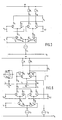
- the invention of the main application is based on the idea that a master-slave D flip-flop, which is coupled in a known manner to a cascade ring so that it works as a frequency divider and then clocks of half the frequency with the phase zero, - ⁇ / 2 and - ⁇ in relation to halved frequency, returns if both the output of the slave (S) and that of the master (M) are used.
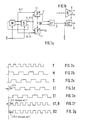
- a cascade which is driven by the input clock T, was proposed in patent applications P 35 46 131 and P 35 46 132 and can be seen on the left in FIG. 1a.
- the clock T is plotted over time in FIG. 2a.
- the output signals of the master flip-flop M can be clearly seen in FIG. 2b with the phase zero and the output of the slave flip-flop S with the phase - ⁇ / 2, shown in FIG. 2c.
- These two signals M, S are applied to the two inputs of a first phase shift element of the usual type ⁇ 1, s. Figure 5 on p. 929 of the literature cited at the beginning, given (input A and input B).
- the phase shifting element In accordance with the set control voltage U r (control V in ), the phase shifting element generates at its output (V out ) a signal which can be set continuously in the range between the phase zero and the phase - ⁇ / 2.
- the output signal ⁇ 1 according to FIG.
- phase shift element ⁇ 2 which is of the same design and which has the slave signal S, ie phase - ⁇ / 2, at its first input and the inverted master signal at its second input M , ie the phase - ⁇ are input, generates a signal 2 at its output which, depending on the control voltage U r, can continuously pass through the range from - ⁇ / 2 to - ⁇ .
- the two phase shifters ⁇ 1 and ⁇ 2 are controlled together by the same control voltage, so that the phase difference between ⁇ 1 and ⁇ 2 can always be kept constant at ⁇ / 2.
- the output signal ⁇ 2 at the output of the second phase shifter is plotted over time in FIG. 2e.
- the two output signals of the phase shift elements ⁇ 1 and ⁇ 2 still have the frequency halved.
- a subsequent frequency doubling with an exclusive OR gate 01 made.
- At the output of this EXOR element there is now a signal at the frequency of the clock T on the input side, but in the example out of phase by a value of approximately - ⁇ / 2 based on this frequency, see FIG. Time diagram 01 according to Figure 2f.
- the phase can now be shifted in the range 0 to - ⁇ .
- the output voltage of the phase shifters ⁇ 1 and ⁇ 2 which is somewhat reduced (by approx. 30%) in the middle phase shift range, is generally regenerated to the binary unit level (0 or 1) by the EXOR element 01.
- buffer amplifiers can be connected downstream of the two phase shifters or the EXOR element (not shown in FIG. 1).
- the EXOR gate 01 is followed by another exclusive OR gate 02, which can be connected to its second input E. If the binary value 0 is present at this input E, a signal which is phase-shifted by 0 to - ⁇ is generated, but if the binary value 1 occurs at the input E, a signal 02, see. Is generated at the output of the second EXOR element.
- Figure 2g generated, which runs in push-pull, that is shifted by - ⁇ . This extends the phase shift range from zero to - ⁇ to - ⁇ to -2 ⁇ . With this circuit arrangement, a continuous phase shift in the range from zero to -2 ⁇ is possible.
- an inverter can also be used instead of the second EXOR element 02, so that, depending on requirements, its output terminal or the output signal of the EXOR element 01 can be used for further processing.
- the inverter can have an adverse effect in that it has additional runtimes that make higher frequencies disturbing. Therefore, it is often cheaper to use a buffer that has an inverting output in addition to the normal output (see FIG. 1b) and in which the signal delay between its input and one of the two outputs is the same. In this case, even at high frequencies, a seamless transition between the two phase ranges 0 ...- ⁇ and - ⁇ ...- 2 ⁇ is possible without overlap.
- Such circuits are common, for example, in the known ECL circuit technology.
- An inverter or a buffer stage with an additional inverting output may be dispensed with if the EXOR gate 01 - as is possible in ECL circuit technology - has an inverting output in addition to the normal output.
- Another possibility is to use an RS flip-flop instead of branch 01, B, 02, which is acted upon at its set or reset inputs by the output signals of the two phase shift elements ⁇ 1, ⁇ 2 and on its inverted and not inverted outputs, the desired signals are phase-shifted by 0 to - ⁇ or - ⁇ to -2 ⁇ .
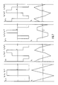
- FIG. 3 shows the basic concept of an adjustable phase shifter of the usual type. 4 shows, plotted against time, the differential output currents i7 minus i8 of the phase shifter for, according to FIG. 3, different current distributions I5 to I6 of the inflows of the two input stages. The input voltages uE1 and uE2 for the two input stages and their output currents i1 i2 or i3 and i4 are also plotted over time. As already indicated above, the phase shifter shown in FIG. 3 is only suitable for shifting sinusoidal clock signals with a not too large amplitude.
- phase shifter circuit which also operates with rectangular signals when driven, is shown in FIGS. 5 and 6.
- the difference compared to the circuit shown in FIG. 3 is the use of a low pass at the circuit output.
- the capacitance C1 is the total capacitance including the parasitic capacitances of the transistors T1 to T4 of the two input stages and the input capacitance of the subsequent EXOR gate.
- FIG. 8 A representation of the output voltage for different current ratios l5 to 10 and I6 to I0 for the non-ideal case, ie not for the limit case of the ideal integrator, is shown in FIG. 8.
- the capacitance C1 is too small or, in other words, the operating frequency is too small.
- a further circuit with an output-side low-pass filter is shown by the phase shifter according to FIG. 6, in which a transimpedance stage for signal regeneration is inserted behind the capacitor C1, by means of which the permissible frequency range can be expanded.
Landscapes
- Physics & Mathematics (AREA)
- Nonlinear Science (AREA)
- Engineering & Computer Science (AREA)
- Microelectronics & Electronic Packaging (AREA)
- Computer Networks & Wireless Communication (AREA)
- Signal Processing (AREA)
- Manipulation Of Pulses (AREA)
- Networks Using Active Elements (AREA)
Applications Claiming Priority (2)
| Application Number | Priority Date | Filing Date | Title |
|---|---|---|---|
| DE3822857 | 1988-07-06 | ||
| DE19883822857 DE3822857C1 (en) | 1987-04-06 | 1988-07-06 | Method and circuit arrangement for producing a phase-shifted clock signal |
Publications (3)
| Publication Number | Publication Date |
|---|---|
| EP0349715A2 true EP0349715A2 (fr) | 1990-01-10 |
| EP0349715A3 EP0349715A3 (en) | 1990-09-26 |
| EP0349715B1 EP0349715B1 (fr) | 1994-01-05 |
Family
ID=6358079
Family Applications (1)
| Application Number | Title | Priority Date | Filing Date |
|---|---|---|---|
| EP89106224A Expired - Lifetime EP0349715B1 (fr) | 1988-07-06 | 1989-04-08 | Procédé et circuit pour produire un signal d'horloge décalé en phase |
Country Status (2)
| Country | Link |
|---|---|
| US (1) | US5015872A (fr) |
| EP (1) | EP0349715B1 (fr) |
Cited By (1)
| Publication number | Priority date | Publication date | Assignee | Title |
|---|---|---|---|---|
| US6910144B2 (en) | 2000-11-30 | 2005-06-21 | Infineon Technologies Ag | Method and configuration for generating a clock pulse in a data processing system having a number of data channels |
Families Citing this family (14)
| Publication number | Priority date | Publication date | Assignee | Title |
|---|---|---|---|---|
| JP3754070B2 (ja) * | 1994-02-15 | 2006-03-08 | ラムバス・インコーポレーテッド | 遅延ロック・ループ |
| US5554945A (en) * | 1994-02-15 | 1996-09-10 | Rambus, Inc. | Voltage controlled phase shifter with unlimited range |
| WO1996008868A2 (fr) * | 1994-09-15 | 1996-03-21 | Philips Electronics N.V. | Circuit de temporisation et systeme de transmission utilisant un tel circuit |
| EP0744832B1 (fr) * | 1995-05-24 | 2001-11-28 | Infineon Technologies AG | Circuit pour la génération d'un signal de sortie orthogonal à un signal d'entrée et utilisation de ce circuit |
| WO1996037952A1 (fr) | 1995-05-26 | 1996-11-28 | Rambus, Inc. | Dephaseur a usage dans un generateur de signal d'horloge en quadrature |
| US5945860A (en) * | 1996-01-04 | 1999-08-31 | Northern Telecom Limited | CLM/ECL clock phase shifter with CMOS digital control |
| DE19544642C1 (de) * | 1995-11-30 | 1997-04-03 | Deutsche Forsch Luft Raumfahrt | Digitaler Phasenschieber |
| US5706484A (en) * | 1995-12-20 | 1998-01-06 | Intel Corporation | Method for eliminating transition direction sensitive timing skews in a source synchronous design |
| US5774001A (en) * | 1995-12-20 | 1998-06-30 | Intel Corporation | Method for eliminating multiple output switching timing skews in a source synchronous design |
| US5723995A (en) * | 1995-12-20 | 1998-03-03 | Intel Corporation | Method for eliminating process variation timing skews in a source synchronous design |
| US6472921B1 (en) * | 2001-05-31 | 2002-10-29 | Siemens Aktiengesellschaft | Delivering a fine delay stage for a delay locked loop |
| DE10132230C2 (de) * | 2001-06-29 | 2003-08-28 | Infineon Technologies Ag | Verfahren und Vorrichtung zur Erzeugung eines Taktausgangssignales |
| DE602004026841D1 (de) * | 2004-05-31 | 2010-06-10 | St Microelectronics Srl | Vorteilerstufe für Hochfrequenzanwendungen |
| US7848220B2 (en) * | 2005-03-29 | 2010-12-07 | Lockheed Martin Corporation | System for modeling digital pulses having specific FMOP properties |
Family Cites Families (6)
| Publication number | Priority date | Publication date | Assignee | Title |
|---|---|---|---|---|
| DE2344152A1 (de) * | 1973-09-01 | 1975-04-10 | Bosch Fernsehanlagen | Verfahren zur einstellbaren verzoegerung von impulsen und schaltungsanordnung zur durchfuehrung des verfahrens |
| US4160217A (en) * | 1976-04-01 | 1979-07-03 | Sony Corporation | Phase locked loop circuit |
| US4663594A (en) * | 1984-09-13 | 1987-05-05 | Motorola, Inc. | Electronic phase shifter circuit and method |
| DE3546132A1 (de) * | 1985-12-24 | 1987-07-02 | Ant Nachrichtentech | Schaltungsanordnung zur erzeugung zweier takte |
| DE3711592A1 (de) * | 1987-04-06 | 1988-10-20 | Ant Nachrichtentech | Verfahren und schaltungsanordnung zur erzeugung eines phasenverschobenen digitalen signales |
| JPS6450611A (en) * | 1987-08-21 | 1989-02-27 | Nec Corp | Phase shifter |
-
1989
- 1989-04-08 EP EP89106224A patent/EP0349715B1/fr not_active Expired - Lifetime
- 1989-07-05 US US07/375,686 patent/US5015872A/en not_active Expired - Fee Related
Cited By (2)
| Publication number | Priority date | Publication date | Assignee | Title |
|---|---|---|---|---|
| US6910144B2 (en) | 2000-11-30 | 2005-06-21 | Infineon Technologies Ag | Method and configuration for generating a clock pulse in a data processing system having a number of data channels |
| DE10061167B4 (de) * | 2000-11-30 | 2005-12-15 | Infineon Technologies Ag | Verfahren zur Erzeugung von Taktsignalen in einem Datenverarbeitungssystem mit einer Vielzahl von Datenkanälen und Anordnung zur Durchführung des Verfahrens |
Also Published As
| Publication number | Publication date |
|---|---|
| EP0349715B1 (fr) | 1994-01-05 |
| US5015872A (en) | 1991-05-14 |
| EP0349715A3 (en) | 1990-09-26 |
Similar Documents
| Publication | Publication Date | Title |
|---|---|---|
| DE4018614C2 (de) | Schaltungsanordnung zur Erzeugung zweier phasenverschobener Ausgangssignale | |
| EP0349715B1 (fr) | Procédé et circuit pour produire un signal d'horloge décalé en phase | |
| DE19838096A1 (de) | Fraktionaler Phasenregelkreis | |
| DE19531748A1 (de) | Spannungsgesteuerter Oszillator | |
| DE2735642C2 (de) | Phasenverriegelungsschleife | |
| DE60033339T2 (de) | Verfahren zur Überwachung des Takts und Vorrichtung zur Datenübertragung, die das Verfahren verwendet | |
| DE69522616T2 (de) | Synchrone Detektion von optischen Signalen | |
| DE2015812A1 (de) | Hochfrequenz Leistungsverstärker | |
| DE2619964A1 (de) | Anordnung zur impuls-zeitlagekorrektur | |
| DE3822857C1 (en) | Method and circuit arrangement for producing a phase-shifted clock signal | |
| WO2013164232A1 (fr) | Convertisseur numérique/analogique à cadencement optique et unité dds équipée d'un tel convertisseur | |
| DE4325896C2 (de) | Phasenstartbare Taktgebervorrichtung | |
| DE2646737C3 (de) | Hilfstraeger-regenerationsschaltung fuer einen farbfernsehempfaenger | |
| DE1591194B1 (de) | Diversity-Empfangssystem | |
| DE2620969C2 (de) | Digital-Analogwandler bei einem Lagemeßsystem | |
| DE19720017B4 (de) | 90°-Phasenschieber | |
| DE3711592C2 (fr) | ||
| EP0465713B1 (fr) | Circuit CMOS pour convertisseur numérique-analogique formateur de moyenne | |
| DE19545435A1 (de) | Linearisierungsschaltungsvorrichtung | |
| EP0004341B1 (fr) | Synchronisation d'un oscillateur local avec un oscillateur de référence | |
| DE3822858A1 (de) | Verfahren und schaltungsanordnung zur erzeugung eines phasenverschobenen taktsignales | |
| DE102007019745A1 (de) | Kaskadierter Phasenschieber | |
| EP0415111B1 (fr) | Alimentation d'un système en impulsions d'horloge de secours pour systèmes digitaux | |
| EP0408969B1 (fr) | Dispositif pour la compensation de temps de propagation et pour la purification de jitter d'un signal de données reçues | |
| DE2636687C2 (de) | Elektronische Schaltungsanordnung zum Umsetzen von in serieller Form eintreffenden Signalen in Parallelform |
Legal Events
| Date | Code | Title | Description |
|---|---|---|---|
| PUAI | Public reference made under article 153(3) epc to a published international application that has entered the european phase |
Free format text: ORIGINAL CODE: 0009012 |
|
| AK | Designated contracting states |
Kind code of ref document: A2 Designated state(s): FR GB IT NL |
|
| PUAL | Search report despatched |
Free format text: ORIGINAL CODE: 0009013 |
|
| AK | Designated contracting states |
Kind code of ref document: A3 Designated state(s): FR GB IT NL |
|
| 17P | Request for examination filed |
Effective date: 19901228 |
|
| 17Q | First examination report despatched |
Effective date: 19921008 |
|
| GRAA | (expected) grant |
Free format text: ORIGINAL CODE: 0009210 |
|
| AK | Designated contracting states |
Kind code of ref document: B1 Designated state(s): FR GB IT NL |
|
| ITF | It: translation for a ep patent filed | ||
| GBT | Gb: translation of ep patent filed (gb section 77(6)(a)/1977) |
Effective date: 19940114 |
|
| ET | Fr: translation filed | ||
| PLBE | No opposition filed within time limit |
Free format text: ORIGINAL CODE: 0009261 |
|
| STAA | Information on the status of an ep patent application or granted ep patent |
Free format text: STATUS: NO OPPOSITION FILED WITHIN TIME LIMIT |
|
| 26N | No opposition filed | ||
| PGFP | Annual fee paid to national office [announced via postgrant information from national office to epo] |
Ref country code: NL Payment date: 19970428 Year of fee payment: 9 |
|
| PGFP | Annual fee paid to national office [announced via postgrant information from national office to epo] |
Ref country code: GB Payment date: 19980327 Year of fee payment: 10 |
|
| PGFP | Annual fee paid to national office [announced via postgrant information from national office to epo] |
Ref country code: FR Payment date: 19980420 Year of fee payment: 10 |
|
| PG25 | Lapsed in a contracting state [announced via postgrant information from national office to epo] |
Ref country code: NL Free format text: LAPSE BECAUSE OF NON-PAYMENT OF DUE FEES Effective date: 19981101 |
|
| NLV4 | Nl: lapsed or anulled due to non-payment of the annual fee |
Effective date: 19981101 |
|
| PG25 | Lapsed in a contracting state [announced via postgrant information from national office to epo] |
Ref country code: GB Free format text: LAPSE BECAUSE OF NON-PAYMENT OF DUE FEES Effective date: 19990408 |
|
| GBPC | Gb: european patent ceased through non-payment of renewal fee |
Effective date: 19990408 |
|
| PG25 | Lapsed in a contracting state [announced via postgrant information from national office to epo] |
Ref country code: FR Free format text: LAPSE BECAUSE OF NON-PAYMENT OF DUE FEES Effective date: 19991231 |
|
| REG | Reference to a national code |
Ref country code: FR Ref legal event code: ST |
|
| PG25 | Lapsed in a contracting state [announced via postgrant information from national office to epo] |
Ref country code: IT Free format text: LAPSE BECAUSE OF NON-PAYMENT OF DUE FEES;WARNING: LAPSES OF ITALIAN PATENTS WITH EFFECTIVE DATE BEFORE 2007 MAY HAVE OCCURRED AT ANY TIME BEFORE 2007. THE CORRECT EFFECTIVE DATE MAY BE DIFFERENT FROM THE ONE RECORDED. Effective date: 20050408 |