EP0349033A2 - Shift register assembly - Google Patents
Shift register assembly Download PDFInfo
- Publication number
- EP0349033A2 EP0349033A2 EP89201548A EP89201548A EP0349033A2 EP 0349033 A2 EP0349033 A2 EP 0349033A2 EP 89201548 A EP89201548 A EP 89201548A EP 89201548 A EP89201548 A EP 89201548A EP 0349033 A2 EP0349033 A2 EP 0349033A2
- Authority
- EP
- European Patent Office
- Prior art keywords
- lead
- gate means
- register
- section
- gate
- Prior art date
- Legal status (The legal status is an assumption and is not a legal conclusion. Google has not performed a legal analysis and makes no representation as to the accuracy of the status listed.)
- Granted
Links
Images
Classifications
-
- G—PHYSICS
- G11—INFORMATION STORAGE
- G11C—STATIC STORES
- G11C19/00—Digital stores in which the information is moved stepwise, e.g. shift registers
- G11C19/28—Digital stores in which the information is moved stepwise, e.g. shift registers using semiconductor elements
- G11C19/287—Organisation of a multiplicity of shift registers
-
- G—PHYSICS
- G11—INFORMATION STORAGE
- G11C—STATIC STORES
- G11C27/00—Electric analogue stores, e.g. for storing instantaneous values
- G11C27/04—Shift registers
Landscapes
- Solid State Image Pick-Up Elements (AREA)
- Transforming Light Signals Into Electric Signals (AREA)
Abstract
Description
- This invention relates to a charge-coupled device (CCD) shift register.
- It is known to use a CCD array as a serial-parallel-serial (SPS) analog shift register for high speed signal acquisition.
- An SPS analog shift register comprises an input serial register, an output serial register, and a parallel register that connects the input serial register to the output serial register. The parallel register is composed of multiple segments, each comprising a serial register, extending between the input register and the output register. An input signal is sampled at an input diode of the SPS shift register and consecutive samples are shifted through the input register. When the input register is full, the samples are shifted into respective segments of the parallel register, emptying the input register. The input register is filled and emptied again, and as each group of samples is shifted into the parallel register the samples that were previously shifted into the parallel register are advanced by one step through the parallel register. Ultimately, each group of samples reaches the output register, and is shifted serially through the output register to an output node of the SPS shift register.
- U.S. Patent No. 4,725,748 issued February 16, 1988 (Hayes, et al) discloses a two-channel SPS analog shift register using a four-phase CCD fabricated on a p-type silicon die having an n-type buried channel region. The input signal is sampled at input diodes of the two channels respectively, by sampling clocks that are of the same frequency but are 180o out of phase with each other, and the charge samples are applied to input registers of the two channels respectively. One of the channels has a lead-in section, which delays the samples taken at the input diode of that channel by one-half the sampling clock period. Therefore, each sample taken by the channel having the additional transfer electrodes enters the serial register of that channel at the same time that the next sample, which is taken by the other channel, enters the shift register of that other channel. Therefore, the two consecutive samples can be clocked through the respective channels simultaneously.
- The effective sampling rate of the two-channel shift register shown in Patent No. 4,725,748 is twice the transfer clock rate. The technique disclosed in Patent No. 4,725,748 may be applied to a two-phase shift register. In the current state of the art, the maximum effective sampling rate that can be achieved using a two-channel shift register based on the teachings of Patent No. 4,725,748 is about 500 Ms/s.
- A preferred embodiment of the present invention in its first aspect is a charge-transfer register comprising a die of semiconductor material having a buried channel region therein, and first gate means and second gate means overlying the buried channel region, the electron potential energy in the buried channel region defining both a potential well and a potential barrier beneath each of the first gate means and the second gate means. The register also comprises means for driving the first gate means and the second gate means with drive signals that are both of the same frequency and are out of phase by an angle that is substantially less than 180o.
- A preferred embodiment of the present invention in its second aspect is a shift register comprising four serial registers each having an input section, a transfer section, and a lead-in section disposed between the input section and the transfer section. The input sections provide respective sequences of charge samples, the four sequences being offset in phase relative to each other by 90o within the cycle of a clock signal. At least one of the serial registers comprises at least first lead-in gate means and second lead-in gate means over the lead-in section, the second lead-in gate means being between the first lead-in gate means and the transfer section. The first lead-in gate means and the second lead-in gate means are each driven at the frequency of the clock signal, the drive signal applied to the second lead-in gate means being retarded in phase relative to that applied to the first lead-in gate means by 90o within the cycle of the clock signal.
- A preferred embodiment of the present invention in its third aspect is a shift register comprising four serial registers each having an input section, a transfer section, and a lead-in section disposed between the input section and the transfer section. The input sections provide respective sequences of charge samples, the four sequences being offset in phase relative to each other by 90o within the cycle of a clock signal. Each serial register comprises at least first and second sets of transfer gates in cyclically repeating sequence over the transfer section, with the first gate of the first set nearer to the input section than any gate of the second set. At least one of the serial registers comprises at least first lead-in gate means and second lead-in gate means over the lead-in section, the second lead-in gate means being between the first lead-in gate means and the transfer section. The transfer gates are driven at the frequency of the clock signal, and the first lead-in gate means and the second lead-in gate means are each driven at the frequency of the clock signal. The drive signal applied to the second lead-in gate means is retarded in phase relative to that applied to the first lead-in gate means by 90o within the cycle of the clock signal.
- For a better understanding of the invention, and to show how the same may be carried into effect, reference will now be made, by way of example, to the accompanying drawings in which:
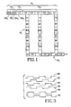
- FIG. 1 is a schematic top plan view of a portion of an integrated circuit,
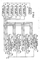
- FIG. 2 is a sectional view of part of that portion of the integrated circuit shown in FIG. 1, and also illustrates parts of three other portions of the integrated circuit, and
- FIG. 3 illustrates the waveforms of drive signals that are applied to gates of the integrated circuit.
- The integrated circuit shown in FIGS. 1 and 2 comprises a die of p-type silicon formed with four n-type buried channel regions. The four buried channel regions are used to implement a two-phase four-channel SPS CCD shift register. To facilitate description of the shift register, the subscripts 1, 2, 3 and 4 are used in connection with the four signal channels respectively of the shift register.
- Each signal channel of the SPS shift register comprises an input serial register 4, a parallel register 16 and an output serial register 18. Part of the input serial register 4 of of each of the four channels is shown in FIG. 2. The four
input serial registers 4₁...4₄ each have aninput section 10, a lead-in section 12 and a transfer section 14. The transfer sections of the four input serial registers respectively are identical and may be implemented in conventional manner. Theinput serial register 4₁, theparallel register 16₁ and the outputserial register 18₁ of one signal channel are shown in FIG. 1. The parallel registers and the output serial registers of the four signal channels are identical and may be implemented in conventional manner. - The part of the buried channel region that is used to implement the input
serial register 4₁ extends from ann+ diffusion 20₁. Thediffusion 20₁ is an input diffusion, which is connected to aninput terminal 21 at which the SPS shift register receives a single-ended input signal. Conductive gates are formed over the buried channel region. The gates are in five sets, designated A, B, C, L and T in FIG. 1. The gates are connected to clock drivers, some of which are shown in FIG. 2. The clock drivers shown in FIG. 2 comprise sampling clock drivers 30-36 andtransfer clock drivers master clock clock 44 so that each sampling clock signal is offset in phase with respect to each of the other signals by an integral (non-zero) multiple of 90o. The transfer clock signals provided by thetransfer clock drivers drivers drivers - The first and
second gates 22 and 24 of each serial register 4 are in theinput section 10 and each such gate is connected to one of the sampling clock drivers 30-36. The lead-in section of each register includes at least two gates. The gates in the lead-in section are connected in pairs, and each such gate pair is connected to one of the sampling clock drivers 30-36. There is one gate pair in the lead-in section of thechannel 2₁, and there are two gate pairs in the lead-in section of each of the channels 2₂ and 2₃, and three gate pairs in the lead-in section of thechannel 2₄. There are multiple gate pairs in the transfer section, alternate gate pairs being connected to thetransfer clock driver 40 and thetransfer clock driver 42. - The conductive gates are made of polysilicon, and alternate gates are formed respectively from a lower level and an upper level of polysilicon, which are applied successively. This method of forming conductive gates is well known in the art. After the lower level gates are formed, and before the upper level gates are formed, an n implantation is carried out so that when the upper level gates have been formed, the electron potential energy beneath the upper level gates of the lead-in and transfer sections is lower than the electron potential energy beneath the lower level gates of those sections, as shown in FIG. 2 by the energy
potential profiles 50₁...50₄. The electron potential energy beneath the upper and lower level gates of the input sections is the same as that beneath the lower level gates of the lead-in and transfer sections. This method of establishing variation in electron potential energy along the length of an n-type buried channel region by use of an n implantation is described in co-pending Patent Application S. N. filed concurrently herewith (Attorney Docket No. USA 4743), the disclosure which is hereby incorporated by reference herein. - Considering, by way of example, the
serial register 4₁, when the drive signals provided by thedrivers gates input diffusion 20₁ diffuses along this conductive path. When the drive signal provided by thedriver 36 goes low, the conductive path beneath thegate 22₁ is broken, trapping a charge sample beneath thegate 24₁. The quantity of charge that is trapped depends on the voltage of the input signal applied to the input terminal of the shift register. The first andsecond gates 22 and 24 of the other threeserial registers register 4₁. Accordingly, the four serial registers allow the input signal to be sampled at four times the frequency of the clock signals. - Referring again to the
register 4₁, thegate pair 60₁ in the lead-in section is connected to thesampling clock driver 34, which provides a clock signal that is 180o out of phase with respect to that provided by thedriver 30. Therefore, the sample beneath thegate 24₁ of the input section is transferred to the well beneath the upper level gate of thegate pair 60₁ when the signal applied to thegate 24₁ goes low and the signal applied to thegate pair 60₁ goes high. The signal provided by thedriver 34 is 180o out of phase with respect to the signal provided by thedriver 40, and therefore when thefirst gate pair 70₁ of the transfer section goes high, thegate pair 60₁ goes low and charge is transferred from the well of the lead-in section to the first well of the transfer section. The charge sample remains in the well of the lead-in section for one-half the period of the sampling clock. - In the case of the
register 4₃, the lead-in section has two gate pairs 60₃ and 62₃, and consequently two wells. Thefirst gate pair 60₃ is connected to thedriver 30 and the second to thedriver 34. When thegate 24₃, which is connected to thedriver 34, goes low, thefirst gate pair 60₃ of the lead-in section goes high and the charge sample is transferred to the first well of the lead-in section. When thefirst gate pair 60₃ goes low, thesecond gate pair 62₃ goes high, and charge is transferred from the first well to the second well. When thesecond gate pair 62₃ goes low, thefirst gate pair 70₃ of the transfer section goes high and the charge is transferred from the second well of the lead-in section to the first well of the transfer section. Accordingly, the charge sample remains in the lead-in section for one period of the sampling clock. - In the case of the
register 4₂, the two gate pairs 60₂ and 62₂ of the lead-in section are connected to thedrivers driver 32 is advanced in phase by 90o with respect to the signal provided by thedriver 34. Therefore, when a charge sample is transferred from the first well of the lead-in section to the second well of the lead-in section, it only remains in the second well for one-quarter of the period of the sampling clock before being transferred to the first well of the transfer section. Accordingly, a charge sample remains in the lead-in section of theregister 4₂ for three-quarters of the sampling clock period. In the case of theregister 4₄, which has three gate pairs 60₄, 62₄ and 64₄ in its lead-in section, a charge sample remains in each of the first and second wells of the lead-in section for one-half the clock period, but it remains in the third well of the lead-in section for only one-quarter of the clock period. - It will therefore be seen that if four samples are taken consecutively by the
registers registers register 4₁, and accordingly the four samples enter the transfer sections of the respective serial registers simultaneously. This allows the four samples to be clocked through the respective channels of the SPS register simultaneously, so that a single set of drivers can be used to perform charge transport, output resetting and output sampling functions for the four channels. By operating in this fashion, the input signal is sampled at four times the sampling clock frequency. Sample rates of 500 to 1000 Msamples/s can be achieved in this manner. - It will be appreciated that the present invention is not restricted to the particular embodiment that has been described and illustrated, and that variations may be made therein without departing from the scope of the invention as defined in the appended claims and equivalents thereof. In particular, it is not necessary that the electron potential energy profile be produced by use of an n implant, which provides wells in the buried channel region, and a p implant, which provides barriers, may be used instead. Also, although four sampling clock drivers are shown, they could be implemented as two sampling clock drivers with differential outputs. Although the invention has been described with reference to a single-ended input signal, a shift register for sampling a differential input signal may be fabricated by providing eight buried channel regions in the die, which each of the four signal channels of the shift register having a positive side and a negative side.
Claims (8)
a die of semiconductor material having a buried channel region therein,
first gate means and second gate means overlying the buried channel region, the electron potential energy in the buried channel region defining both a potential well and a potential barrier beneath each of the first gate means and the second gate means, and
means for driving the first gate means and the second gate means with drive signals that are at the same frequency and are out of phase by an angle that is substantially less than 180o.
at least first lead-in gate means and second lead-in gate means over the lead-in section, the second lead-in gate means being between the first lead-in gate means and the transfer section, and
means for driving the first lead-in gate means and the second lead-in gate means each at the frequency of the clock signal, the drive signal applied to the second lead-in gate means being advanced in phase relative to that applied to the first lead-in gate means by 90o within the cycle of the clock signal.
four serial registers each having an input section for providing a sequence of charge samples, the four sequences of charge samples provided by the input sections of the four serial registers respectively being offset in phase relative to each other by 90o within the cycle of a clock signal, a transfer section, and a lead-in section disposed between the input section and the transfer section, and comprising at least first and second sets of transfer gates in cyclically repeating sequence over the transfer section, with a first gate of the first set nearer to the input section than any gate of the second set, and at least one of the serial registers comprising:
at least first lead-in gate means and second lead-in gate means over the lead-in section, the second lead-in gate means being between the first lead-in gate means and the transfer section,
means for driving the transfer gates at the frequency of said clock signal, and
means for driving the first lead-in gate means and the second lead-in gate means each at the frequency of the clock signal, the drive signal applied to the second lead-in gate means being retarded in phase relative to that applied to the first lead-in gate means by 90o within the cycle of the clock signal.
Applications Claiming Priority (2)
| Application Number | Priority Date | Filing Date | Title |
|---|---|---|---|
| US213554 | 1988-06-30 | ||
| US07/213,554 US4951302A (en) | 1988-06-30 | 1988-06-30 | Charge-coupled device shift register |
Publications (3)
| Publication Number | Publication Date |
|---|---|
| EP0349033A2 true EP0349033A2 (en) | 1990-01-03 |
| EP0349033A3 EP0349033A3 (en) | 1990-11-28 |
| EP0349033B1 EP0349033B1 (en) | 1994-01-19 |
Family
ID=22795550
Family Applications (1)
| Application Number | Title | Priority Date | Filing Date |
|---|---|---|---|
| EP89201548A Expired - Lifetime EP0349033B1 (en) | 1988-06-30 | 1989-06-14 | Shift register assembly |
Country Status (3)
| Country | Link |
|---|---|
| US (1) | US4951302A (en) |
| EP (1) | EP0349033B1 (en) |
| JP (1) | JPH0245941A (en) |
Families Citing this family (6)
| Publication number | Priority date | Publication date | Assignee | Title |
|---|---|---|---|---|
| JPH043436A (en) * | 1990-04-20 | 1992-01-08 | Fuji Photo Film Co Ltd | Ccd delay line |
| US5294982A (en) * | 1991-12-24 | 1994-03-15 | National Captioning Institute, Inc. | Method and apparatus for providing dual language captioning of a television program |
| US5200983A (en) * | 1992-04-17 | 1993-04-06 | Tektronix, Inc. | Fiso analog signal acquisition system employing CCD array storage |
| JPH07232258A (en) * | 1994-02-23 | 1995-09-05 | Ryobi Ltd | Casting method using electromagnetic pump |
| US5937025A (en) * | 1997-03-21 | 1999-08-10 | Dalsa, Inc. | High speed CCD bus structure |
| US6091619A (en) * | 1999-04-23 | 2000-07-18 | Tektronix, Inc. | Array architecture for long record length fast-in slow-out (FISO) analog memory |
Citations (3)
| Publication number | Priority date | Publication date | Assignee | Title |
|---|---|---|---|---|
| US3819959A (en) * | 1970-12-04 | 1974-06-25 | Ibm | Two phase charge-coupled semiconductor device |
| US3935477A (en) * | 1973-04-23 | 1976-01-27 | Bell Telephone Laboratories, Incorporated | Analog inverter for use in charge transfer apparatus |
| US4223233A (en) * | 1977-05-26 | 1980-09-16 | Raytheon Company | Charge transfer device input circuitry |
Family Cites Families (10)
| Publication number | Priority date | Publication date | Assignee | Title |
|---|---|---|---|---|
| GB1457253A (en) * | 1972-12-01 | 1976-12-01 | Mullard Ltd | Semiconductor charge transfer devices |
| DE2501934C2 (en) * | 1974-01-25 | 1982-11-11 | Hughes Aircraft Co., Culver City, Calif. | Method for operating a charge-coupled semiconductor component and charge-coupled semiconductor component for carrying out this method |
| US3913077A (en) * | 1974-04-17 | 1975-10-14 | Hughes Aircraft Co | Serial-parallel-serial ccd memory with interlaced storage |
| US3944990A (en) * | 1974-12-06 | 1976-03-16 | Intel Corporation | Semiconductor memory employing charge-coupled shift registers with multiplexed refresh amplifiers |
| US4211937A (en) * | 1976-01-23 | 1980-07-08 | Tokyo Shibaura Electric Co., Ltd. | Multi-channel charge coupled transfer device |
| US4118795A (en) * | 1976-08-27 | 1978-10-03 | Texas Instruments Incorporated | Two-phase CCD regenerator - I/O circuits |
| US4205283A (en) * | 1978-10-10 | 1980-05-27 | The United States Of America As Represented By The Secretary Of The Army | Signal delay system |
| US4521896A (en) * | 1982-05-14 | 1985-06-04 | Westinghouse Electric Co. | Simultaneous sampling dual transfer channel charge coupled device |
| US4508975A (en) * | 1982-09-28 | 1985-04-02 | Rca Corporation | Pulse duration modulator using charge coupled devices |
| US4648072A (en) * | 1985-05-06 | 1987-03-03 | Tektronix, Inc. | High speed data acquisition utilizing multiplex charge transfer devices |
-
1988
- 1988-06-30 US US07/213,554 patent/US4951302A/en not_active Expired - Fee Related
-
1989
- 1989-06-14 EP EP89201548A patent/EP0349033B1/en not_active Expired - Lifetime
- 1989-06-23 JP JP1162487A patent/JPH0245941A/en active Pending
Patent Citations (3)
| Publication number | Priority date | Publication date | Assignee | Title |
|---|---|---|---|---|
| US3819959A (en) * | 1970-12-04 | 1974-06-25 | Ibm | Two phase charge-coupled semiconductor device |
| US3935477A (en) * | 1973-04-23 | 1976-01-27 | Bell Telephone Laboratories, Incorporated | Analog inverter for use in charge transfer apparatus |
| US4223233A (en) * | 1977-05-26 | 1980-09-16 | Raytheon Company | Charge transfer device input circuitry |
Also Published As
| Publication number | Publication date |
|---|---|
| EP0349033B1 (en) | 1994-01-19 |
| US4951302A (en) | 1990-08-21 |
| JPH0245941A (en) | 1990-02-15 |
| EP0349033A3 (en) | 1990-11-28 |
Similar Documents
| Publication | Publication Date | Title |
|---|---|---|
| CA1068395A (en) | Charge coupled imager | |
| US4928158A (en) | Solid-state image sensor having a plurality of horizontal transfer portions | |
| IL46895A (en) | C c d memory with interlaced storage | |
| WO1991015079A1 (en) | Image sensor | |
| US4206371A (en) | CCD with differently doped substrate regions beneath a common electrode | |
| US4236830A (en) | CCD Parallel-serial and serial-parallel charge transfer method and apparatus | |
| EP0349033A2 (en) | Shift register assembly | |
| EP0350091B1 (en) | Tilted channel charge-coupled device | |
| US4199691A (en) | CCD Multiple channel network | |
| EP0096166B1 (en) | Charge coupled device and circuit arrangement for its operation | |
| EP0553869B1 (en) | Method for transferring charge, charge transfer device and solid state image sensing device using the same | |
| US4777519A (en) | Charge transfer device | |
| JPH0373140B2 (en) | ||
| EP0161023B1 (en) | Charge-coupled semiconductor device with dynamic control | |
| US4010485A (en) | Charge-coupled device input circuits | |
| US5923061A (en) | CCD charge splitter | |
| JPS58175A (en) | Semiconductor device | |
| JPS61179574A (en) | Charge coupled device | |
| US5760430A (en) | Charge transfer device and solid-state imaging apparatus using the same device | |
| US4891826A (en) | Method of operating a charge-coupled device to reduce spillback | |
| US5900769A (en) | Two-dimensional CCD having storage cells for withdrawing charge packets from transfer channels during horizontal scan periods | |
| US4733407A (en) | Charge-coupled device | |
| US5146480A (en) | Sampling an analog signal voltage using fill and spill input in charge transfer device | |
| JPS62242363A (en) | Charge transfer device | |
| US5943095A (en) | Method for operating charge-coupled device at high speed |
Legal Events
| Date | Code | Title | Description |
|---|---|---|---|
| PUAI | Public reference made under article 153(3) epc to a published international application that has entered the european phase |
Free format text: ORIGINAL CODE: 0009012 |
|
| AK | Designated contracting states |
Kind code of ref document: A2 Designated state(s): CH LI NL |
|
| PUAL | Search report despatched |
Free format text: ORIGINAL CODE: 0009013 |
|
| AK | Designated contracting states |
Kind code of ref document: A3 Designated state(s): CH LI NL |
|
| 17P | Request for examination filed |
Effective date: 19901115 |
|
| 17Q | First examination report despatched |
Effective date: 19921117 |
|
| GRAA | (expected) grant |
Free format text: ORIGINAL CODE: 0009210 |
|
| AK | Designated contracting states |
Kind code of ref document: B1 Designated state(s): CH LI NL |
|
| PLBE | No opposition filed within time limit |
Free format text: ORIGINAL CODE: 0009261 |
|
| STAA | Information on the status of an ep patent application or granted ep patent |
Free format text: STATUS: NO OPPOSITION FILED WITHIN TIME LIMIT |
|
| 26N | No opposition filed | ||
| PGFP | Annual fee paid to national office [announced via postgrant information from national office to epo] |
Ref country code: NL Payment date: 19960529 Year of fee payment: 8 |
|
| PGFP | Annual fee paid to national office [announced via postgrant information from national office to epo] |
Ref country code: CH Payment date: 19960606 Year of fee payment: 8 |
|
| PG25 | Lapsed in a contracting state [announced via postgrant information from national office to epo] |
Ref country code: LI Free format text: LAPSE BECAUSE OF NON-PAYMENT OF DUE FEES Effective date: 19970630 Ref country code: CH Free format text: LAPSE BECAUSE OF NON-PAYMENT OF DUE FEES Effective date: 19970630 |
|
| PG25 | Lapsed in a contracting state [announced via postgrant information from national office to epo] |
Ref country code: NL Effective date: 19980101 |
|
| REG | Reference to a national code |
Ref country code: CH Ref legal event code: PL |
|
| NLV4 | Nl: lapsed or anulled due to non-payment of the annual fee |
Effective date: 19980101 |