EP0348738A2 - Procédé de détermination non destructive d'inhomogénéités électroniques dans des couches semi-conductrices - Google Patents
Procédé de détermination non destructive d'inhomogénéités électroniques dans des couches semi-conductrices Download PDFInfo
- Publication number
- EP0348738A2 EP0348738A2 EP89110809A EP89110809A EP0348738A2 EP 0348738 A2 EP0348738 A2 EP 0348738A2 EP 89110809 A EP89110809 A EP 89110809A EP 89110809 A EP89110809 A EP 89110809A EP 0348738 A2 EP0348738 A2 EP 0348738A2
- Authority
- EP
- European Patent Office
- Prior art keywords
- laser beam
- measuring
- semiconductor layer
- modulated optical
- modulated
- Prior art date
- Legal status (The legal status is an assumption and is not a legal conclusion. Google has not performed a legal analysis and makes no representation as to the accuracy of the status listed.)
- Ceased
Links
Images

Classifications
-
- G—PHYSICS
- G01—MEASURING; TESTING
- G01N—INVESTIGATING OR ANALYSING MATERIALS BY DETERMINING THEIR CHEMICAL OR PHYSICAL PROPERTIES
- G01N21/00—Investigating or analysing materials by the use of optical means, i.e. using sub-millimetre waves, infrared, visible or ultraviolet light
- G01N21/84—Systems specially adapted for particular applications
- G01N21/88—Investigating the presence of flaws or contamination
- G01N21/95—Investigating the presence of flaws or contamination characterised by the material or shape of the object to be examined
- G01N21/9501—Semiconductor wafers
-
- G—PHYSICS
- G01—MEASURING; TESTING
- G01N—INVESTIGATING OR ANALYSING MATERIALS BY DETERMINING THEIR CHEMICAL OR PHYSICAL PROPERTIES
- G01N21/00—Investigating or analysing materials by the use of optical means, i.e. using sub-millimetre waves, infrared, visible or ultraviolet light
- G01N21/17—Systems in which incident light is modified in accordance with the properties of the material investigated
- G01N21/1717—Systems in which incident light is modified in accordance with the properties of the material investigated with a modulation of one or more physical properties of the sample during the optical investigation, e.g. electro-reflectance
-
- G—PHYSICS
- G01—MEASURING; TESTING
- G01N—INVESTIGATING OR ANALYSING MATERIALS BY DETERMINING THEIR CHEMICAL OR PHYSICAL PROPERTIES
- G01N21/00—Investigating or analysing materials by the use of optical means, i.e. using sub-millimetre waves, infrared, visible or ultraviolet light
- G01N21/17—Systems in which incident light is modified in accordance with the properties of the material investigated
- G01N21/55—Specular reflectivity
-
- G—PHYSICS
- G01—MEASURING; TESTING
- G01N—INVESTIGATING OR ANALYSING MATERIALS BY DETERMINING THEIR CHEMICAL OR PHYSICAL PROPERTIES
- G01N21/00—Investigating or analysing materials by the use of optical means, i.e. using sub-millimetre waves, infrared, visible or ultraviolet light
- G01N21/84—Systems specially adapted for particular applications
- G01N21/88—Investigating the presence of flaws or contamination
- G01N21/95—Investigating the presence of flaws or contamination characterised by the material or shape of the object to be examined
- G01N21/9501—Semiconductor wafers
- G01N21/9505—Wafer internal defects, e.g. microcracks
Definitions
- the invention relates to a method for the non-destructive determination of electronic inhomogeneities of a semiconductor layer by measuring the modulated optical reflectivity of a laser beam of a different wavelength induced by irradiation of the semiconductor layer with intensity-modulated laser radiation.
- optical measuring methods can be used to detect electronic inhomogeneities, e.g. caused by defects in crystalline semiconductor layers or by ion implantations.
- Optical measuring methods that use the effect of modulated optical reflectivity (MOR technology) to determine the electronic inhomogeneities of a semiconductor layer are described in the publications Appl. Phys. Letters 47 (6), 1985, pages 584-586, Appl. Phys. Letters 47 (5), 1985, pages 498-500, J. Appl. Phys. 61 (1), 1987, pages 240-248 and in the diploma thesis of St. Wurm at the TU Kunststoff, Physics Department Insitut E-13, April 1988 and are described in commercially available measuring devices, e.g. "Therma Probe 200" from Therma Wave Inc. (USA).
- MOR technology modulated optical reflectivity
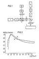
- FIG. 1 shows the block diagram of a test setup for determining the modulated optical reflectivity of a test sample 1.
- An Argon Arg ion laser 10 serves to excite the test sample 1 (pump laser).
- the argon+ ion laser beam striking the test sample 1 has a wavelength of 488 nm with a power of 5 mW.
- the argon+ ion laser beam is focused onto the measurement sample 1 by means of a beam expander 8 and a microscope objective 7.
- a HeNe laser 2 delivers the measuring laser beam with a wavelength of 632.8 nm at a power of 2 to 3 mW.
- the HeNe laser beam passes through a number of optical components such as a beam expander 3, a polarizing beam splitter 4, a ⁇ / 4 plate 5 and is coupled in through the microscope objective 7 with the aid of a semitransparent mirror 6 parallel to the modulated argonl ion laser beam and hits confocal with this onto the measurement sample 1.
- the HeNe laser beam reflected back from the measurement sample 1 again passes through the ⁇ / 4 plate and is directed by the polarizing beam splitter 4 through an interference filter 11 onto a photocell 12, with which the measurement signal is detected.
- a lock-in amplifier 13 which uses the modulation frequency of the Argon+ ion laser beam as the reference frequency, represents the output voltage as the amplitude of the sample reflectivity for HeNe laser light that is periodically modulated at a frequency of 1 MHz.
- curve 14 shows the dependence of the modulated optical reflectivity MOR for HeNe laser radiation on the implantation dose D when measuring the modulated reflectivity of an ion-implanted silicon layer.
- Curve 15 shows the behavior obtained from a theoretical model. The illustration is taken from the diploma thesis by St. Wurm, in which experimental work and theoretical considerations are further described.
- the determination of implantation doses in semiconductor layers by measuring the modulated optical reflectivity by means of the described method is suitable for the range of low implantation doses of approx. 1010 cm ⁇ 2 to 1013 cm ⁇ 2.
- an amorphous layer is formed on the semiconductor surface, the thickness of which depends both on the dose and on the implantation energy. There is therefore a layer system with different optical properties. Because of the interference effects due to reflection of the measuring laser beam in different layers, it is not possible to clearly assign the measuring signal to the implantation dose D.
- the measurement signal R is the layer thickness d of the implanted semiconductor layer, d. H.
- the object of the invention is to provide a method for non-destructive Determine the determination of the electronic inhomogeneities of a semiconductor layer, with which the density of the electronic inhomogeneities can be determined precisely.
- the method is said to be particularly suitable for implantation control in the area of high implantation doses (above approx. 1015cm ⁇ 2).
- This object is achieved by a method of the type mentioned in the introduction in that the modulated optical reflectivity of a laser radiation with a wavelength in the range from 200 to 345 nm is measured as a measure of the density of the electronic inhomogeneities.
- the common semiconductor materials such as silicon, germanium, gallium arsenide, gallium antimonide and indium phosphide, have a strong absorption capacity, the depth of penetration of the measuring laser beam into the semiconductor layer is greatly reduced (e.g. about 10 nm in silicon).
- the electronic inhomogeneities present in the semiconductor layer can therefore be determined by measurement in the surface area of the semiconductor layer which is influenced by the electronic inhomogeneities.
- the measurement setup from FIG. 1 is used as an exemplary embodiment for teaching the invention, the following measurement parameters applying: Pump laser: Argon+ ion laser, wavelength 488 nm, power 5 mW. Measuring laser: helium-cadmium laser, wavelength 325 nm, power 8 mW, e.g. helium-cadmium laser type multi mode 356 XM, omnichrome (company Laser 200, Kunststoff). Diameter of the measuring point 1 ⁇ m, penetration depth 10 nm. Sample: Implanted silicon layer, implantation dose greater than 1015 ions cm ⁇ 2.
- the method can be used for the entire usual implantation dose range and in particular also for structured semiconductor wafers. With a measuring spot in the order of magnitude of 1 ⁇ m, the method according to the invention can be used to carry out spatially resolved measurements.
- the method according to the invention can be used for the analysis of any semiconductor layers in which there are characteristic electronic inhomogeneities.
- the invention also includes special also the application for the determination of residual damage in crystalline semiconductor layers.
Landscapes
- General Health & Medical Sciences (AREA)
- Health & Medical Sciences (AREA)
- Life Sciences & Earth Sciences (AREA)
- Chemical & Material Sciences (AREA)
- Analytical Chemistry (AREA)
- Biochemistry (AREA)
- Physics & Mathematics (AREA)
- General Physics & Mathematics (AREA)
- Immunology (AREA)
- Pathology (AREA)
- Testing Or Measuring Of Semiconductors Or The Like (AREA)
- Investigating Or Analysing Materials By Optical Means (AREA)
- Investigating Materials By The Use Of Optical Means Adapted For Particular Applications (AREA)
Applications Claiming Priority (2)
| Application Number | Priority Date | Filing Date | Title |
|---|---|---|---|
| DE3822346 | 1988-07-01 | ||
| DE3822346 | 1988-07-01 |
Publications (2)
| Publication Number | Publication Date |
|---|---|
| EP0348738A2 true EP0348738A2 (fr) | 1990-01-03 |
| EP0348738A3 EP0348738A3 (fr) | 1991-04-03 |
Family
ID=6357779
Family Applications (1)
| Application Number | Title | Priority Date | Filing Date |
|---|---|---|---|
| EP19890110809 Ceased EP0348738A3 (fr) | 1988-07-01 | 1989-06-14 | Procédé de détermination non destructive d'inhomogénéités électroniques dans des couches semi-conductrices |
Country Status (3)
| Country | Link |
|---|---|
| US (1) | US5034611A (fr) |
| EP (1) | EP0348738A3 (fr) |
| JP (1) | JP2974689B2 (fr) |
Families Citing this family (13)
| Publication number | Priority date | Publication date | Assignee | Title |
|---|---|---|---|---|
| JP2626275B2 (ja) * | 1991-02-28 | 1997-07-02 | 富士通株式会社 | イオン注入モニタリング方法 |
| US5717518A (en) * | 1996-07-22 | 1998-02-10 | Kla Instruments Corporation | Broad spectrum ultraviolet catadioptric imaging system |
| GB2357158B (en) * | 1996-07-22 | 2001-07-18 | Kla Instr Corp | A method of inspecting objects for defects |
| US6323951B1 (en) * | 1999-03-22 | 2001-11-27 | Boxer Cross Incorporated | Apparatus and method for determining the active dopant profile in a semiconductor wafer |
| US6812717B2 (en) * | 2001-03-05 | 2004-11-02 | Boxer Cross, Inc | Use of a coefficient of a power curve to evaluate a semiconductor wafer |
| US6940592B2 (en) * | 2001-10-09 | 2005-09-06 | Applied Materials, Inc. | Calibration as well as measurement on the same workpiece during fabrication |
| US7126690B2 (en) * | 2002-09-23 | 2006-10-24 | Therma-Wave, Inc. | Modulated reflectance measurement system using UV probe |
| US6878559B2 (en) * | 2002-09-23 | 2005-04-12 | Applied Materials, Inc. | Measurement of lateral diffusion of diffused layers |
| US6963393B2 (en) * | 2002-09-23 | 2005-11-08 | Applied Materials, Inc. | Measurement of lateral diffusion of diffused layers |
| US20040253751A1 (en) * | 2003-06-16 | 2004-12-16 | Alex Salnik | Photothermal ultra-shallow junction monitoring system with UV pump |
| US20050112853A1 (en) * | 2003-11-26 | 2005-05-26 | Raymond Kuzbyt | System and method for non-destructive implantation characterization of quiescent material |
| US11295969B2 (en) | 2018-11-27 | 2022-04-05 | International Business Machines Corporation | Hybridization for characterization and metrology |
| US11480868B2 (en) | 2019-03-22 | 2022-10-25 | International Business Machines Corporation | Determination of optical roughness in EUV structures |
Family Cites Families (4)
| Publication number | Priority date | Publication date | Assignee | Title |
|---|---|---|---|---|
| US4352016A (en) * | 1980-09-22 | 1982-09-28 | Rca Corporation | Method and apparatus for determining the quality of a semiconductor surface |
| US4511800A (en) * | 1983-03-28 | 1985-04-16 | Rca Corporation | Optical reflectance method for determining the surface roughness of materials in semiconductor processing |
| US4679946A (en) * | 1984-05-21 | 1987-07-14 | Therma-Wave, Inc. | Evaluating both thickness and compositional variables in a thin film sample |
| US4652757A (en) * | 1985-08-02 | 1987-03-24 | At&T Technologies, Inc. | Method and apparatus for optically determining defects in a semiconductor material |
-
1989
- 1989-06-14 EP EP19890110809 patent/EP0348738A3/fr not_active Ceased
- 1989-06-27 JP JP1165161A patent/JP2974689B2/ja not_active Expired - Fee Related
-
1990
- 1990-07-10 US US07/560,228 patent/US5034611A/en not_active Expired - Lifetime
Also Published As
| Publication number | Publication date |
|---|---|
| EP0348738A3 (fr) | 1991-04-03 |
| US5034611A (en) | 1991-07-23 |
| JPH0246745A (ja) | 1990-02-16 |
| JP2974689B2 (ja) | 1999-11-10 |
Similar Documents
| Publication | Publication Date | Title |
|---|---|---|
| DE19681741B4 (de) | Verbesserter optischer Beanspruchungsgenerator und -detektor | |
| EP0348738A2 (fr) | Procédé de détermination non destructive d'inhomogénéités électroniques dans des couches semi-conductrices | |
| DE69032373T2 (de) | Vermögensmodulierte laservorrichtungen | |
| EP0011708B1 (fr) | Méthode et dispositif pour mesurer la planéité, la rugosité ou le rayon de courbure d'une surface à mesurer | |
| DE19733890C2 (de) | Verfahren zum Vermessen eines Mediums und Vorrichtung dazu | |
| DE3116611C2 (de) | Vorrichtung zur Messung von Halbleitereigenschaften | |
| DE3908155A1 (de) | Vorrichtung und verfahren zur vermessung duenner dielektrischer schichten | |
| DE2533906A1 (de) | Beruehrungslose oberflaechen-pruefvorrichtung | |
| DE3240234A1 (de) | Oberflaechenprofil-interferometer | |
| DE69114256T2 (de) | Verfahren und Apparat zur optischen Messung. | |
| DE19781728B4 (de) | Optisches Verfahren und System zum Bestimmen mechanischer Eigenschaften eines Materials | |
| EP0011724B1 (fr) | Procédé de détermination directe de constantes magnétostrictives et dispositif pour sa mise en oeuvre | |
| DE2854057A1 (de) | Ebenheits-messeinrichtung | |
| DE4400097B4 (de) | Vorrichtung zum Abschätzen der Lebensdauer von Halbleiter-Material | |
| EP0400373B1 (fr) | Procédé pour la détermination de la résolution spatiale de la longueur de diffusion de porteurs minoritaires de charge dans un corps cristallin semi-conducteur à l'aide d'une cellule électrolytique | |
| DE2853816A1 (de) | Ebenheits-messeinrichtung | |
| DE69232288T2 (de) | Messung von materialeigenschaften mit optisch induzierten phononen | |
| DE60310318T2 (de) | Vorrichtung und Verfahren zur zerstörungsfreien Messung der Eigenschaften eines Halbleitersubstrats | |
| EP0396811B1 (fr) | Méthode et dispositif de représentation et mesure avec une phase exacte de champs d'ondes élastiques à l'aide d'une sonde à laser | |
| DE602004005347T2 (de) | Einrichtung und verfahren zur eindringungsfreien detektion und messung der eigenschaften eines mediums | |
| EP0435829B1 (fr) | Arrangement pour l'analyse d'ondes thermiques dans des systèmes en couches | |
| DE19840725B4 (de) | Verfahren und interferenzoptische Messeinrichtung zur optoelektronischen Vermessung der Mikrostrukturen eines mikroelektronischen Bauelementes | |
| EP0803062B2 (fr) | Procede et dispositif permettant de determiner l'epaisseur, la conductibilite et/ou la qualite de contact de couches appliquees sur des substrats | |
| JP3210489B2 (ja) | シリコンウェーハ及びその酸化膜耐圧の評価方法 | |
| Knite | Study of optical properties of PLZT ceramics by laser calorimetry |
Legal Events
| Date | Code | Title | Description |
|---|---|---|---|
| PUAI | Public reference made under article 153(3) epc to a published international application that has entered the european phase |
Free format text: ORIGINAL CODE: 0009012 |
|
| AK | Designated contracting states |
Kind code of ref document: A2 Designated state(s): DE FR GB IT NL |
|
| PUAL | Search report despatched |
Free format text: ORIGINAL CODE: 0009013 |
|
| 17P | Request for examination filed |
Effective date: 19901220 |
|
| AK | Designated contracting states |
Kind code of ref document: A3 Designated state(s): DE FR GB IT NL |
|
| 17Q | First examination report despatched |
Effective date: 19930426 |
|
| STAA | Information on the status of an ep patent application or granted ep patent |
Free format text: STATUS: THE APPLICATION HAS BEEN REFUSED |
|
| 18R | Application refused |
Effective date: 19940507 |