EP0347778B1 - Diode avec un comportement modifié pendant la coupure - Google Patents
Diode avec un comportement modifié pendant la coupure Download PDFInfo
- Publication number
- EP0347778B1 EP0347778B1 EP89111018A EP89111018A EP0347778B1 EP 0347778 B1 EP0347778 B1 EP 0347778B1 EP 89111018 A EP89111018 A EP 89111018A EP 89111018 A EP89111018 A EP 89111018A EP 0347778 B1 EP0347778 B1 EP 0347778B1
- Authority
- EP
- European Patent Office
- Prior art keywords
- region
- diode
- cathode
- zone
- anode
- Prior art date
- Legal status (The legal status is an assumption and is not a legal conclusion. Google has not performed a legal analysis and makes no representation as to the accuracy of the status listed.)
- Expired - Lifetime
Links
- 239000004065 semiconductor Substances 0.000 claims description 6
- 230000004888 barrier function Effects 0.000 claims 4
- 239000002800 charge carrier Substances 0.000 description 14
- 230000000903 blocking effect Effects 0.000 description 6
- 238000000034 method Methods 0.000 description 4
- 230000006378 damage Effects 0.000 description 3
- 238000010586 diagram Methods 0.000 description 2
- 230000015556 catabolic process Effects 0.000 description 1
- 239000003795 chemical substances by application Substances 0.000 description 1
- 238000006731 degradation reaction Methods 0.000 description 1
- 238000009792 diffusion process Methods 0.000 description 1
- 230000000694 effects Effects 0.000 description 1
- 230000000149 penetrating effect Effects 0.000 description 1
- 229910052710 silicon Inorganic materials 0.000 description 1
- 239000010703 silicon Substances 0.000 description 1
- 230000007704 transition Effects 0.000 description 1
Images

Classifications
-
- H—ELECTRICITY
- H10—SEMICONDUCTOR DEVICES; ELECTRIC SOLID-STATE DEVICES NOT OTHERWISE PROVIDED FOR
- H10D—INORGANIC ELECTRIC SEMICONDUCTOR DEVICES
- H10D8/00—Diodes
- H10D8/80—PNPN diodes, e.g. Shockley diodes or break-over diodes
Definitions
- the invention relates to a diode according to the preamble of the claim.
- Such a diode also known as a PSN structure
- a diode is known, for example, from the book “Semiconductors” by A. Porst, published in 1973 by the publishing house of Siemens AG, Berlin and Kunststoff, pp. 121 to 124. It is disadvantageous, however, that when such a diode is switched off, that is to say when it is switched from the on state in which a certain load current flows through it to the off state, a very high reverse voltage can develop at the diode, which can be caused by Leads to their destruction.
- the reverse current which flows through the diode during the transition into the blocking state and is applied by an external circuit and which flows through the diode in the cathode-anode direction when a reverse voltage is applied between the cathode-side and the anode-side electrode, as long as there are still charge carriers to be cleared out in the central region. can suddenly break off at the moment when there are no more charge carriers to be cleared outside the space charge zone at the pn junction between the anode region and the central region. This then results in a very steep rise in the reverse voltage at the diode, which can cause the destruction mentioned above.
- a Shockley diode is known from the European application with the publication number EP 0 021 899 A1, in which between a highly doped, n-conducting cathode region and a highly doped, p-conducting anode region not only a weakly doped n-conducting middle region, but a p-conducting base zone is inserted between the middle region and the cathode region and the middle region has a higher doping than the rest of the middle region both at the cathode-side end and at the anode-side end n-type zone.
- the invention has for its object to provide a diode of the type mentioned, which can be switched from the on state to the blocking state, that is to say commutated, without tearing off the reverse current. This is achieved according to the invention by training according to the characterizing part of the patent claim.
- the advantage that can be achieved with the invention is, in particular, that when the diode is switched off, sufficient charge carriers are available to maintain the reverse current required for commutation until the reverse voltage at the diode has completely built up.
- the semiconductor diode shown in FIG. 1 consists of a disk-shaped, doped semiconductor body, for example made of silicon, which has an external p-type anode region 1 and an external, n-type cathode region 2.
- the cathode region 2 is contacted in a first main area 3 by a cathode-side electrode 4, which has a connection K is provided.
- the anode region 1 is contacted in a second main area 5 by an anode-side electrode 6, which has a connection A.
- 7 denotes an n-conducting central region, which is separated from the anode region 1 by a pn junction 8.
- a p-type base zone 11 is inserted into the stop zone 10 so that it extends up to extends to the first main surface 3 and is surrounded on all sides in the lateral direction by the stop zone 10.
- the cathode region 2 is in turn inserted into the base zone 11 in such a way that it extends to the main surface 3 and is surrounded on all sides in the lateral direction by the base zone 11.
- FIG. 2 shows the doping profile of the diode according to FIG. 1 in a diagram, on the horizontal axis of which the distances d from all locations lying on a straight line oriented perpendicular to the main surface 5 are plotted from this main surface 5, while in the vertical direction the doping concentrations n belonging to these locations are plotted.
- the partial profile of the anode region 1 produced by an edge-side p-diffusion is indicated, whose doping concentration in the vicinity of the main surface 5 is approximately 1019cm ⁇ 3.
- the basic doping of the semiconductor body which corresponds to the central region 7 and is approximately 1013 to 1014cm ⁇ 3, is indicated by a straight line 13, while the stop zone 10, which has a doping concentration of approximately 1015 to 1016cm ⁇ 3 in the vicinity of the interface 3 , are characterized by the partial profile 14, the p-type base zone 11 by the partial profile 15 and the cathode region 2 by the partial profile 16.
- the doping concentration of 2 in the vicinity of the main surface 3 is approximately 1020cm ⁇ 3, that of the base zone 11 approximately 4.1016 to 1018cm ⁇ 3.
- the pn junction 8 and the pn junction 17 between the p-type base zone 11 and the stop zone 10 are identified in FIG. 2, as is the interface 9, by their distances d8, d9 and d17.
- FIG. 3 shows the time dependence of the reverse current i Di and the reverse voltage u Di when a conventional PSN diode consisting only of parts 1, 7 and 2 is switched off.
- the sections on the time axis t each correspond to 5 »s, the sections on the vertical axis each 50 A or 2.5 kV.
- the space charge zone continues to advance upwards, it can now appear that it reaches the upper clearance zone before the full reverse voltage has developed between K and A. If one assumes that this occurs at a point in time at which the return current i Di has a size given by the curve point 19, then i Di breaks off suddenly, which is illustrated by the vertical curve branch 20. After a phase of overshoot 21, the reverse current has dropped to a reverse current that is no longer recognizable in FIG. 3. However, the sudden current cut at 20 causes a large rise 22 of the reverse voltage, which leads to a peak value 23, which causes the destruction of the diode or of the circuit parts connected to it. Of the Overshoot phase 21 of the reverse current i Di corresponds to an overshoot phase 24 of the diode voltage u Di before u Di reaches the value of the reverse voltage present in the external circuit.
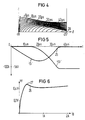
- FIG. 4 shows a family of curves which illustrate the charge carrier degradation in the central region 7 between the horizontal cross-sectional planes with the distances d8 and d17 (cf. FIG. 2) from the main surface 5.
- the parameters of the individual curves correspond to the microseconds past after the blocking voltage was applied.
- the area under a certain curve represents the quantity of the charge carriers still remaining in the central region 7 at the time specified by the parameter, the position of this curve also characterizing the zone in which these charge carriers are located.
- the charge carriers are degraded further and further in the direction of d17 starting from d8, the lower clearing zone, which first builds up at the distance d8 from the main surface 5, extends further and further upwards into the central region 7. Since charge carriers are repeatedly supplied from the p-type base zone 2 to the central region 7, in contrast to the clearing process, no upper clearing zone can be formed in a conventional PSN diode. Therefore, even after about 40 »s, a charge carrier residue remains in a zone 28, which directly adjoins the cross-sectional plane identified by d17. However, this means that the space charge zone building up at the pn junction 8 and thus the lower clearing zone can expand as far as is necessary to achieve the desired reverse voltage between A and K without i Di and thus an extremely large reverse voltage 23 could build up.
- Fig. 5 shows, in deviation from Fig. 3, the course of the reverse current i Di 'and the diode voltage u Di ' of a diode according to the invention, wherein a given by the curve branch 25 all gradual decrease of i Di 'and a corresponding gradual build-up of u Di ' to the value of the reverse voltage present in the outer circuit can be determined.
- the forward voltage u F of a diode according to the invention in volts as a function of the forward current i D in amperes. It can be seen from this that the pn junction 17 initially blocks at low currents. Only after the central region 7 has been flooded with charge carriers, the forward voltage in the curve part 26 drops and in the further course corresponds to that of a conventional PSN diode. In order to keep the local voltage maximum indicated by 27 low, the stop zone 10 is doped on the one hand so that it has a doping concentration n which differs only slightly from the p-type base zone 2.
- the space charge zone building up at the pn junction 17 in the on state has only a small expansion and can therefore only absorb a small voltage in the forward direction.
- the gain of the npn transistor consisting of the semiconductor zones 10 and 11 and of the cathode region 2 is chosen to be large. Taken together, both measures have the effect that the aforementioned flooding of the central region 7 occurs even at low values of the forward current i D.
- the stop zone 10 also has the purpose of preventing the space charge zone building up in the blocking state at the pn junction 8 from expanding so far in the direction of the p-conducting base zone 11 before the blocking voltage between A and K is reached that it achieves this, which would mean a "punch through".
Landscapes
- Bipolar Integrated Circuits (AREA)
- Bipolar Transistors (AREA)
- Thyristors (AREA)
Claims (1)
- Diode comportant un corps semiconducteur qui comporte une région de cathode (2) conductrice du type n, placée en contact avec une électrode (4) située côté cathode, une région d'anode (1) conductrice de type p, placée en contact avec une électrode (6) située côté anode, et une région médiane (7) conductrice du type n, qui est plus faiblement dopée que lesdites deux régions et est séparée de la région d'anode (1) par une jonction pn (8), une zone, située côté cathode, de la région médiane constituant une zone d'arrêt (10) conductrice du type n, qui est plus fortement dopée que le reste de la région médiane (7),
caractérisée par le fait
que dans la zone d'arrêt (10) est insérée une zone de base (11) conductrice du type p, qui s'étend jusqu'à une surface principale (3) située côté cathode et est enserrée de tous côtés, dans une direction latérale, par la zone d'arrêt (10), et que la région de cathode (2) est insérée dans la zone de base (11) de telle sorte qu'elle s'étend jusqu'à la surface principale (3) située du côté cathode et est entourée de tous côtés, dans une direction latérale, par la zone de base (11), et que le dopage de la zone de base (11) conductrice de type p est légèrement supérieur au dopage de la zone d'arrêt (10), mais est nettement inférieur au dopage de la région de cathode ou d'anode (2 ou 1).
Applications Claiming Priority (2)
| Application Number | Priority Date | Filing Date | Title |
|---|---|---|---|
| DE3820917 | 1988-06-21 | ||
| DE3820917 | 1988-06-21 |
Publications (3)
| Publication Number | Publication Date |
|---|---|
| EP0347778A2 EP0347778A2 (fr) | 1989-12-27 |
| EP0347778A3 EP0347778A3 (fr) | 1991-02-06 |
| EP0347778B1 true EP0347778B1 (fr) | 1995-05-31 |
Family
ID=6356916
Family Applications (1)
| Application Number | Title | Priority Date | Filing Date |
|---|---|---|---|
| EP89111018A Expired - Lifetime EP0347778B1 (fr) | 1988-06-21 | 1989-06-16 | Diode avec un comportement modifié pendant la coupure |
Country Status (3)
| Country | Link |
|---|---|
| EP (1) | EP0347778B1 (fr) |
| JP (1) | JP2751103B2 (fr) |
| DE (1) | DE58909264D1 (fr) |
Families Citing this family (2)
| Publication number | Priority date | Publication date | Assignee | Title |
|---|---|---|---|---|
| FR2737343B1 (fr) * | 1995-07-28 | 1997-10-24 | Ferraz | Composant limiteur de courant et procede de realisation |
| DE19860581A1 (de) * | 1998-12-29 | 2000-07-06 | Asea Brown Boveri | Halbleiterelement und Verfahren zur Herstellung |
Family Cites Families (2)
| Publication number | Priority date | Publication date | Assignee | Title |
|---|---|---|---|---|
| FR2458905A1 (fr) * | 1979-06-06 | 1981-01-02 | Silicium Semiconducteur Ssc | Diode de shockley et son procede de fabrication |
| GB2113907B (en) * | 1981-12-22 | 1986-03-19 | Texas Instruments Ltd | Reverse-breakdown pn junction devices |
-
1989
- 1989-06-16 JP JP1154384A patent/JP2751103B2/ja not_active Expired - Lifetime
- 1989-06-16 DE DE58909264T patent/DE58909264D1/de not_active Expired - Lifetime
- 1989-06-16 EP EP89111018A patent/EP0347778B1/fr not_active Expired - Lifetime
Also Published As
| Publication number | Publication date |
|---|---|
| JPH0237780A (ja) | 1990-02-07 |
| DE58909264D1 (de) | 1995-07-06 |
| EP0347778A3 (fr) | 1991-02-06 |
| EP0347778A2 (fr) | 1989-12-27 |
| JP2751103B2 (ja) | 1998-05-18 |
Similar Documents
| Publication | Publication Date | Title |
|---|---|---|
| EP0621640B1 (fr) | Dispositif de puissance à semi-conducteur | |
| DE2707744C2 (fr) | ||
| DE3633161C2 (fr) | ||
| DE4208695C2 (de) | Leitungsmodulations MOSFET | |
| CH668505A5 (de) | Halbleiterbauelement. | |
| DE2437428A1 (de) | Schutzschaltung | |
| DE3521079C2 (fr) | ||
| EP0106059B1 (fr) | Commutateur semi-conducteur muni d'un thyristor à blocage par la gâchette | |
| EP0929910A1 (fr) | Transistor a effet de champ mos vertical de puissance | |
| DE69028161T2 (de) | Halbleiteranordnung mit isoliertem Gate | |
| EP0520355B1 (fr) | Composant semi-conducteur de puissance à commande d'extinction et procédé de sa fabrication | |
| DE1912192A1 (de) | Halbleiterschaltelement mit Gleichrichterdiodenaufbau | |
| DE3838964C2 (fr) | ||
| DE3612367C2 (fr) | ||
| EP0347778B1 (fr) | Diode avec un comportement modifié pendant la coupure | |
| DE2329398A1 (de) | In sperrichtung leitende thyristoreinrichtung, sowie verfahren zu deren herstellung | |
| DE4438896A1 (de) | Halbleiterdiode mit Elektronenspender | |
| DE2534703A1 (de) | Abschaltbarer thyristor | |
| EP0344514A2 (fr) | Thyristor à commande d'extinction | |
| DE19936636A1 (de) | Schutzstruktur für eine integrierte Halbleiterschaltung zum Schutz vor elektrostatischer Entladung | |
| DE3000891A1 (de) | Halbleiterbaustein mit gattersteuerung | |
| DE3112941A1 (de) | Thyristor mit innerer stromverstaerkung und verfahren zu seinem betrieb | |
| DE2608432C3 (de) | Leistungsdiode | |
| DE4342482C2 (de) | Schnelle Leistungshalbleiterbauelemente | |
| DE69421749T2 (de) | Halbleiterschalter mit IGBT und Thyristor |
Legal Events
| Date | Code | Title | Description |
|---|---|---|---|
| PUAI | Public reference made under article 153(3) epc to a published international application that has entered the european phase |
Free format text: ORIGINAL CODE: 0009012 |
|
| AK | Designated contracting states |
Kind code of ref document: A2 Designated state(s): CH DE FR GB LI SE |
|
| PUAL | Search report despatched |
Free format text: ORIGINAL CODE: 0009013 |
|
| 17P | Request for examination filed |
Effective date: 19901205 |
|
| AK | Designated contracting states |
Kind code of ref document: A3 Designated state(s): CH DE FR GB LI SE |
|
| 17Q | First examination report despatched |
Effective date: 19931011 |
|
| GRAA | (expected) grant |
Free format text: ORIGINAL CODE: 0009210 |
|
| AK | Designated contracting states |
Kind code of ref document: B1 Designated state(s): CH DE FR GB LI SE |
|
| REF | Corresponds to: |
Ref document number: 58909264 Country of ref document: DE Date of ref document: 19950706 |
|
| GBT | Gb: translation of ep patent filed (gb section 77(6)(a)/1977) |
Effective date: 19950814 |
|
| ET | Fr: translation filed | ||
| PLBE | No opposition filed within time limit |
Free format text: ORIGINAL CODE: 0009261 |
|
| STAA | Information on the status of an ep patent application or granted ep patent |
Free format text: STATUS: NO OPPOSITION FILED WITHIN TIME LIMIT |
|
| 26N | No opposition filed | ||
| PGFP | Annual fee paid to national office [announced via postgrant information from national office to epo] |
Ref country code: CH Payment date: 19970912 Year of fee payment: 9 |
|
| PGFP | Annual fee paid to national office [announced via postgrant information from national office to epo] |
Ref country code: SE Payment date: 19980615 Year of fee payment: 10 |
|
| PG25 | Lapsed in a contracting state [announced via postgrant information from national office to epo] |
Ref country code: LI Free format text: LAPSE BECAUSE OF NON-PAYMENT OF DUE FEES Effective date: 19980630 Ref country code: CH Free format text: LAPSE BECAUSE OF NON-PAYMENT OF DUE FEES Effective date: 19980630 |
|
| REG | Reference to a national code |
Ref country code: CH Ref legal event code: PL |
|
| PG25 | Lapsed in a contracting state [announced via postgrant information from national office to epo] |
Ref country code: SE Free format text: THE PATENT HAS BEEN ANNULLED BY A DECISION OF A NATIONAL AUTHORITY Effective date: 19990629 |
|
| EUG | Se: european patent has lapsed |
Ref document number: 89111018.1 |
|
| REG | Reference to a national code |
Ref country code: GB Ref legal event code: IF02 |
|
| PGFP | Annual fee paid to national office [announced via postgrant information from national office to epo] |
Ref country code: GB Payment date: 20060615 Year of fee payment: 18 |
|
| PGFP | Annual fee paid to national office [announced via postgrant information from national office to epo] |
Ref country code: FR Payment date: 20060619 Year of fee payment: 18 |
|
| GBPC | Gb: european patent ceased through non-payment of renewal fee |
Effective date: 20070616 |
|
| REG | Reference to a national code |
Ref country code: FR Ref legal event code: ST Effective date: 20080229 |
|
| PG25 | Lapsed in a contracting state [announced via postgrant information from national office to epo] |
Ref country code: GB Free format text: LAPSE BECAUSE OF NON-PAYMENT OF DUE FEES Effective date: 20070616 |
|
| PG25 | Lapsed in a contracting state [announced via postgrant information from national office to epo] |
Ref country code: FR Free format text: LAPSE BECAUSE OF NON-PAYMENT OF DUE FEES Effective date: 20070702 |
|
| PGFP | Annual fee paid to national office [announced via postgrant information from national office to epo] |
Ref country code: DE Payment date: 20080807 Year of fee payment: 20 |