EP0347480A1 - Elektrophotographisches und optisches Speichersystem - Google Patents
Elektrophotographisches und optisches Speichersystem Download PDFInfo
- Publication number
- EP0347480A1 EP0347480A1 EP88109941A EP88109941A EP0347480A1 EP 0347480 A1 EP0347480 A1 EP 0347480A1 EP 88109941 A EP88109941 A EP 88109941A EP 88109941 A EP88109941 A EP 88109941A EP 0347480 A1 EP0347480 A1 EP 0347480A1
- Authority
- EP
- European Patent Office
- Prior art keywords
- medium
- writing
- light beam
- reading light
- particles
- Prior art date
- Legal status (The legal status is an assumption and is not a legal conclusion. Google has not performed a legal analysis and makes no representation as to the accuracy of the status listed.)
- Withdrawn
Links
- 230000015654 memory Effects 0.000 title claims abstract description 56
- 230000003287 optical effect Effects 0.000 title claims abstract description 14
- 239000002245 particle Substances 0.000 claims abstract description 97
- 230000004044 response Effects 0.000 claims abstract description 12
- 239000000758 substrate Substances 0.000 claims abstract description 7
- 229920001169 thermoplastic Polymers 0.000 claims abstract description 7
- 239000004416 thermosoftening plastic Substances 0.000 claims abstract description 7
- 239000011159 matrix material Substances 0.000 claims abstract description 4
- 239000013598 vector Substances 0.000 claims abstract description 4
- 239000013078 crystal Substances 0.000 claims description 7
- 230000003750 conditioning effect Effects 0.000 claims description 6
- 238000012545 processing Methods 0.000 claims description 6
- 230000035945 sensitivity Effects 0.000 claims description 6
- 239000011521 glass Substances 0.000 claims description 5
- 238000001514 detection method Methods 0.000 claims description 3
- 238000010438 heat treatment Methods 0.000 claims description 3
- 230000001360 synchronised effect Effects 0.000 claims description 2
- 230000002401 inhibitory effect Effects 0.000 claims 1
- 230000010287 polarization Effects 0.000 abstract description 2
- 238000000034 method Methods 0.000 description 5
- 230000008901 benefit Effects 0.000 description 4
- 239000000463 material Substances 0.000 description 4
- 230000006870 function Effects 0.000 description 3
- 230000001427 coherent effect Effects 0.000 description 2
- 230000008569 process Effects 0.000 description 2
- 241000220225 Malus Species 0.000 description 1
- 230000005540 biological transmission Effects 0.000 description 1
- 230000008859 change Effects 0.000 description 1
- 238000010276 construction Methods 0.000 description 1
- 238000013500 data storage Methods 0.000 description 1
- 238000010586 diagram Methods 0.000 description 1
- 125000000664 diazo group Chemical group [N-]=[N+]=[*] 0.000 description 1
- 238000005286 illumination Methods 0.000 description 1
- 230000006872 improvement Effects 0.000 description 1
- 238000002955 isolation Methods 0.000 description 1
- 239000007788 liquid Substances 0.000 description 1
- 230000007257 malfunction Effects 0.000 description 1
- 238000004519 manufacturing process Methods 0.000 description 1
- 230000005055 memory storage Effects 0.000 description 1
- QSHDDOUJBYECFT-UHFFFAOYSA-N mercury Chemical compound [Hg] QSHDDOUJBYECFT-UHFFFAOYSA-N 0.000 description 1
- 229910052753 mercury Inorganic materials 0.000 description 1
- 238000012986 modification Methods 0.000 description 1
- 230000004048 modification Effects 0.000 description 1
- 238000012856 packing Methods 0.000 description 1
- 230000002093 peripheral effect Effects 0.000 description 1
- 239000004033 plastic Substances 0.000 description 1
- 239000007787 solid Substances 0.000 description 1
- 239000002904 solvent Substances 0.000 description 1
- 239000007921 spray Substances 0.000 description 1
- 238000012546 transfer Methods 0.000 description 1
- 238000001429 visible spectrum Methods 0.000 description 1
Images

Classifications
-
- G—PHYSICS
- G11—INFORMATION STORAGE
- G11B—INFORMATION STORAGE BASED ON RELATIVE MOVEMENT BETWEEN RECORD CARRIER AND TRANSDUCER
- G11B11/00—Recording on or reproducing from the same record carrier wherein for these two operations the methods are covered by different main groups of groups G11B3/00 - G11B7/00 or by different subgroups of group G11B9/00; Record carriers therefor
- G11B11/08—Recording on or reproducing from the same record carrier wherein for these two operations the methods are covered by different main groups of groups G11B3/00 - G11B7/00 or by different subgroups of group G11B9/00; Record carriers therefor using recording by electric charge or by variation of electric resistance or capacitance
Definitions
- the present invention relates to computer mass memory devices.
- the primary mass memory storage devices used with computers today, whether they be mainframe, minicomputers or microcomputers are magnetic tapes and discs. Even with a mainframe computer which might utilize a bank of 14 inch diameter hard discs, the memory capacity with 7 such discs is approximately 350 megabytes. Since a byte has 8 bits, this produces a total memory capacity of slightly less than 3 gigabits. While this is a substantial amount of memory, the size and cost of the hard discs involved and the equipment necessary to operate the disc is substantial. To achieve this quantity of storage capacity using floppy discs would require over 1,000 discs and is impractical.
- CD-ROMs While optical compact discs, known as CD-ROMs, are currently being discussed and can provide storage capacity in the large amounts mentioned above, they have inherent disadvantages in that the medium used for recording is generally non-erasable or rewritable. Further technically more, the CD-ROMS have inherent limitations in accuracy and speed because the CD-ROM uses a platter which must be mechanically rotated much like a record so that the appropriate portion of the rotating platter can be read. Read head alignment problems and the time required for the mechanical operation involved slow the read process down and add the chance for error and malfunction. Of course, the limitation of being a read only memory is in itself enough to make a CD-ROM useless in situations where data must be written to storage and as the computer is operating.
- the speed of writing to and reading from memory is also a consideration.
- the write speed is approximately 20 megahertz.
- the write speed is significantly less.
- the speed at which today's computers operate and the expected operating speeds of future generation computers require an increased speed of data storage and retrieval so that the central processing unit of the computer is not forced to wait or to perform unnecessary shifts between jobs to more economically use the waiting time while the disc drive head is moving to the location where the desired information is to be stored or read, and while the writing or reading takes place.
- the memory system should be operable at write and read speeds far in excess of those possible today with hard discs and with a smaller bit error rate than presently possible.
- the memory system should be erasable as well as provide other advantages.
- the present invention fulfills these needs, and further provides other related advantages.
- the present invention resides in an optical memory system for storage and retrieval of digital data.
- the memory system includes a source of writing light having a first wavelength less than a threshold wavelength, and a source of reading light having a second wavelength greater than the threshold wavelength.
- Modulation means . are provided for modulating the writing light by a write digital signal containing the digital data to be stored.
- Means are also provided for forming the writing light into a writing light beam, and means are provided for forming the reading light into a reading light beam.
- the invention further includes means for deflecting the writing and reading light beams along a first axis in response to a first control signal, and means for deflecting the beams along a second transverse axis at an angle to the first axis in response to a second control signal.
- Lens means are included for focusing the writing and reading light beams to a focal point with a focal plane therethrough.
- the memory system includes a stationary medium manufactured of a dry film having submicron electrically photosensitive particles embedded in a thermal plastic layer mounted on a substantially transparent electrically conducting substrate.
- the particles are insensitive to light with a wavelength greater than the threshold wavelength.
- the particles are initially uncharged and the film is sensitive to light after receiving an initial surface charge.
- the uncharged particles acquire a charge at the expense of the surface charge upon being struck by the writing light beam. Regions of the medium with the charged particles and with the uncharged particles cause differing conditions of the reading light beam. Passage of the reading light beam through the charge particles corresponds to a recorded information bit of the digital data at one binary logic state and passage through the uncharged particles corresponds to a recorded information bit of the digital data at the other binary logic state.
- a fixed mask is positioned substantially in the focal plane of the lens means and in juxtaposition with the medium, between the medium and the lens means.
- the mask is substantially opaque to the writing and reading light beams with a plurality of apertures substantially transparent to the beams.
- the apertures define the extent of the regions of the medium with the charged and uncharged particles.
- Each of the apertures has a size to admit sufficient energy when exposed to the writing light beam for a predetermined time period to exceed a sensitivity threshold value of the medium and charge the particles in the corresponding region of the medium to produce charge particles.
- the apertures are arranged in a plurality of rows aligned with the first axis and positioned one row adjacent to the other in the direction of the second axis.
- the memory system further includes detector means positioned to be exposed to the reading light beam after passing through the mask apertures and the medium.
- the detector means is responsive to the incident of the reading light beam thereon and insensitive to the writing light beam, and detects conditioning of the reading light beam corresponding to passage through one of the regions of the medium with the charged particles, and to passage through one of the regions of the medium with the uncharged particles.
- the detector means further generates a read digital data signal containing the stored digital data from the medium. As such, the binary logic state of a recorded information bit corresponding to one of the regions of the medium is determined.
- the means for generating -the first control signal to detect the writing and reading light beams to scan along a selected one of the rows of the apertures in the direction of the first axis at a selected scan speed.
- the selected scan speed for the writing light beam is such as to expose each of the apertures to the writing light beam for at least the predetermined time period to charge the particles in the corresponding region of the medium to produce charged particles.
- the optical memory system further includes means for generating the second control signal to selectively deflect the writing and reading light beams to the selected row of the apertures.
- the memory system also has means for substantially uniformly charging a surface of the film with the initial charge prior to exposure to the writing light beam.
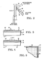
- the present invention is embodied in an optical memory system, indicated generally by reference numeral 10, for the storage of digital data.
- the memory system 10 utilizes an electrophotographic dry film material as a recording medium 12.
- the medium 12 has submicron electrically photosensitive particles 14 embedded in a thermoplastic layer 16 mounted on a substantially transparent electrically conducting substrate 18.
- the particles 14 are insensitive to light with a wavelength greater than .480 microns.
- the particles 14 are initially uncharged and the medium becomes sensitive to light only after receiving an initial surface charge.
- a Corona charging device 22 which extends along one length of the medium is moved laterally across the surface of the medium to apply a uniform charge intensity across the surface, as shown in Figure 3.
- the initially uncharged particles 14 acquire a charge at the expense of the surface charge upon being struck by the light.
- the light used is a writing light beam modulated with a digital data signal.
- the thermoplastic layer 14 and conductive substrate 18 are mounted on a transparent glass backing 24. Additional details concerning the operation of the medium 12 with the present invention will be described below. It is noted that unlike when the film material is used as photographic film, liquid solvent or heat, and by so keeping the medium in an undeveloped state, the medium can be repeatedly charged, erased and recharged.
- the electrophotographic material used in the preferred embodiment as the medium 12 is known as Xerox Dry Microfilm (XDM) and is described in greater detail in U.S. patent Nos. 3,357,989; 3,542,545; 3,648,607; 3,671,282; 3,720,513; 3,816,118; 3,979,210; 3,982,936; 3,985,560; 4,013,462; 4,014,695; 4,028,101; 4,040,826; 4,055,418, which are incorporated herein by reference.
- XDM Xerox Dry Microfilm
- the optical memory system 10 further includes a source 26 of continuous wave monochromatic writing light in the visible light range having a wavelength of less than .480 microns.
- a modulator 28 amplitude modulates the writing light at about a 20 megahertz rate according to a write data input signal on line 30 which embodies the digital data to be stored by the storage medium 12.
- the writing light source 26 is a non-coherent mercury lamp operating at a 0.4 micron wavelength.
- Collimation optics 32 form the modulated writing light into a substantially collimated writing light beam which is projected onto a cube beamsplitter 34 for transmission therethrough.
- the write data input signal is provided by an input/output (I/O) device 35a controlled by a central processing unit (CPU) 35b of the computer with which the memory system 10 is operating.
- I/O input/output
- CPU central processing unit
- the memory system 10 also includes a source 36 of near infrared, coherent and polarized reading light having a wavelength of greater than .480 microns.
- the reading light source 36 is a GaAlAs laser operating at a 0.82 micron wavelength.
- the reading light source 36 may provide constant illumination and need not be switched on and off during operation of the memory system, even when the system is in a writing mode. Additionally, since the medium 12 is photosensitive to only the visible spectrum writing light, the near infrared reading light beam can pass through the medium without altering or modifying the stored charge on the particles 14, thus permitting repeated readings of the stored data.
- the reading light produced by the source 36 is projected through collimation optics 38 to form a substantially collimated reading light beam which is projected onto beamsplitter 34.
- a reflected beam of the reading light beam and the transmitted writing light beam project from the beamsplitter along a single path for both the writing light beam and the reading light beam.
- a beam stop 40 is positioned to intercept the reading light beam transmitted through the beamsplitter.
- the reading light beam is used only to read information from the memory medium 12, and the writing light beam is used only to write information to the medium.
- the writing light beam has a wavelength greater than a threshold wavelength for the medium 12 above which the medium is photosensitive to light.
- the reading light beam has a wavelength which is below the threshold, and thus the medium is insensitive to the reading light beam.
- a horizontal deflector 42 is positioned along the path to deflect which ever of the writing or reading light beam is present along a horizontal axis in response to a horizontal deflector drive signal provided by control circuitry, indicated generally in Figure 1 by reference numeral 44.
- the deflector 42 is a solid state device having a bimorphic piezoelectric crystal electronically controlled by a horizontal deflector drive signal provided by the control circuitry 44.
- the deflector drive signal causes deformation of the bimorphic crystal and thus causes the writing/reading light beam which is incident upon a reflective aluminized surface 46 mounted on one side of the bimorphic crystal to scan along a horizontal axis at a selected scan speed.
- a vertical deflector 50 of somewhat similar construction to horizontal deflector 42 except that the writing/reading light beam passes through the bimorphic crystal.
- the vertical deflector 50 deflects the writing/reading light beam along a vertical axis substantially orthogonal to the horizontal axis in response to a vertical deflector drive signal provided by the control circuitry 44. With appropriate drive signals to the horizontal deflector 42 and the vertical deflector 50, the writing/reading light beam can be caused to scan horizontally or vertically, across any desired portion of the medium 12.
- the writing/reading light beam passes through the vertical deflector 50, it passes through a horizontal cylindrical lens 52 and then through a vertical cylindrical lens 54 which condition the light beam and focus it to a focal point with a focal plane passing therethrough.
- a fixed mask 56 is positioned substantially in the focal plane and in juxtaposition with the medium 12.
- the mask 56 is bonded to a side of the medium 12 which is toward the lenses 52 and 54.
- the mask is substantially opaque to the writing and reading light beams except for a matrix of horizontal rows and vertical columns of substantially transparent light admitting apertures 58 therethrough as is best shown in Figure 5.
- the apertures 58 are circular transmissive portions one micron (i.e., 1.0 X 10 ⁇ 6 meters) in diameter spaced apart on two micron centers, both along the rows and between the rows. With this arrangement, 25 X 106 apertures can be positioned in a matrix of 1.0 cm2 in size having 5,000 rows and 5 000 columns of apertures.
- each aperture 58 defines the extent of a correspondingly sized region of the medium 12 which may have charged or uncharged particles.
- the charged or uncharged state of the particles is used to indicate whether the information stored in the region is a binary "1" or a binary "0", and the state of the particles may be detected using the reading light beam.
- the focal plane mask 56 is manufactured using a diazo material which is developed using a photolithographic technique to form the opaque portions of the mask and the transmissive apertures 58. Other suitable techniques may be used to manufacture the mask.
- the focal plane mask 56 By use of the focal plane mask 56, the focusing problems that have heretofore been encountered are eliminated since the apertures 58 serve as aperture stops.
- the apertures 58 have a diameter which is preferably greater than the wavelength of both the writing light and reading light moving through it so that no defraction problems are encountered.
- the writing light and the reading light have wavelengths of 0.4 and 0.82 microns, respectively, and the apertures have a diameter of 1.0 microns. It is noted that it may be possible to increase the density of the medium 12 by reducing the diameter of the apertures or the spacing between apertures, or both. It has been found that the film medium 12 being used in the presently preferred embodiment of the invention has sufficient resolution through use of the focal plane mask 56, that increased information packing can be achieved without diffraction problems.
- the apertures 58 of the mask 56 define regions of the medium 12 which have not been struck by the writing light beam and hence have particles 14 which retain their initial uncharged state or have been struck by the writing light beam and hence have particles which have acquired a charge at the expense of the surface charge on the medium surface 20.
- Regions of the medium 12 with the charged particles and regions with the uncharged particles cause differing phase velocities of propagation for orthagonal elements of the reading light beam which results in angular rotation of the resultant electric and magnetic field vectors as it passes through the region.
- the electric and magnetic fields are rotated upon passing through a region with charged particles by a first degree of rotation, and upon passing through a region with uncharged particles by a second degree of rotation detectably different from the first degree of rotation.
- the electric and magnetic fields of the reading light beam are rotated as a result of the initial charge placed upon the surface 20 of the medium 12.
- An even greater rotation is realized when the reading light beam passes through a region which has charged particles. This is because the initial surface charge might be at 100 volts while the region which has charged particles might be at 120 volts.
- the higher voltage is the result of the additional charge applied by photons impinging upon the photosensitive particles and imparting additional energy thereto.
- a region with charge particles and the first degree of rotation of the electric and magnetic fields of the reading light beam passing therethrough correspond to a binary "1"
- a region with uncharged particles and a lesser resulting second degree of rotation correspond to a binary "0”.
- each of the apertures 58 in the mask 56 must have a minimum opening size which is related to the time period the writing light beam will impinge on the medium through the aperture.
- the opening size must be large enough to admit sufficient energy when exposed to the writing light beam to exceed the sensitivity threshold value of the medium.
- the time period during which the writing light beam impinges upon the medium depends upon the scan rate of the beam, which is controlled by the control circuitry 44 and which will be described in more detail below.
- the reading light beam passes through the medium and then through a spherical lens 60 which focuses the reading light beam onto a light detector 62, which in the preferred embodiment of the invention is a light detecting photodiode having associated light detection circuitry, indicated by reference numeral 63.
- the light detector 62 generates an indicator signal indicating detection of the reading light beam, and provides the indicator signal to a pulse conditioning comparator 66.
- the photodiode is sensitive to the reading light beam incident thereon, but is insensitive to light at the wavelength of the writing light beam.
- the light detector 62 and circuitry 63 is a conventional OPIC light detector, such as model number IS006 manufactured by Sharp which includes both a light detecting element and peripheral circuits integrated onto one chip.
- the compensator 64 Positioned between the light detector 62 and the lens 60, and in the path of the reading light beam, is a Senarmont polarization compensator 64.
- the compensator 64 includes associated conventional circuitry (not shown).
- the compensator 64 detects and measures the angular rotation of the electric and magnetic field of the reading light beam by measuring the reading light beam intensity relative to a predetermined reference after passing through one of the regions of the medium 12 defined by one of the apertures 58.
- the reading light beam intensity will vary as a function of the degree of angular rotation of the electric and magnetic field vectors as predicted by the well-known Malus' law.
- the reference is based upon the rotation experienced by the reading light beam upon passing through a region of uncharged particles 14.
- the compensator 64 based upon the sensed phase difference between the reading light beam passing through the charged and uncharged regions, generates a data indicating signal on a line 65 to the light detector circuitry 63.
- the data indicating signal effectively modulates the indicator signal amplitude from the light detector 62 and attenuates the indicator signal if a rotation is detected indicative of a recorded information bit of stored digital data at the binary logic state "0".
- An electronic signal amplitude comparator 66 monitors the indicator signal and by comparing the indicator signal to a predetermined amplitude threshold level, will produce a binary "1" output only when the indicator signal, and hence the detected degree of rotation corresponding to passage of the reading light beam through a region of charged particles, exceeds that predetermined threshold indicating a recorded information bit of "1".
- the output of the comparator 66 is a read digital data signal containing the digital data which was stored in the regions of the medium 12 scanned by the reading light beam.
- the read digital data signal is provided to the computer I/O device 35a.
- a Corotron 68 extends the full vertical length of the medium and is selectively movable across the horizontal width of the medium.
- the Corotron 68 is a Corona charging device (as was the device 22 described with respect to Figure 3) and has a back deflector 69 which essentially evenly sprays the surface 20 of the medium 18 with electrons to thereby provide a uniform charge intensity across the surface. After the initial charge is provided to the medium prior to any exposure with the writing light beam, the Corotron 68 is moved out of the path of the writing/reading light beam.
- the medium 12 used with the invention is sensitive to temperatures elevated above normal ambient temperatures and the memory system 10 includes an erasure conditioner 70 which is a heatable shoe positioned adjacent to the glass backing 24 of the medium 12.
- the erasure conditioner heats a correspondingly sized selected portion of the medium 12 to a sufficiently elevated temperature to allow the charged particles in the corresponding portion of the medium to yield their charge and resume an uncharged state when subjected to a reversed polarity field. Since glass is used as the backing 24 (see Figures 3 and 4), the heat is transmitted primarily transversely through the glass, but not laterally so as to enable isolation of adjacent portions of the medium from the heat.
- the erasure conditioner is a 1 cm2 foot which. is selectively heated to heat the corresponding portion of the medium 12 to 70°C or better. At about 70°C, the medium 12 is erased in approximately five seconds, and if the temperature is elevated somewhat, the erasure process can be completed more quickly.
- the Corotron charging device 68 is passed across the surface 20 of the medium corresponding to the portion heated, and a reverse polarity charge is applied thereto (i.e., reversed compared to that of the initial charge). This effectively removes the charge on the particles in that portion of the medium 12.
- the polarity of the Corotron 68 is changed back to that necessary to apply the initial charge, and an initial charge is applied to the surface of the erased portion of the medium 12 to, render the particles 14 in that portion photosensitive.
- the erased portion of the medium is now ready for storage of new digital data based upon the writing light beam impinging upon the medium and the photosensitive particles which have been relieved of their prior charge again being charged upon the incident thereon of the writing light beam.
- the photosensitive particles 14 retain their charge and establish a charged field in a region of the medium 12 without any physical deformation to the medium. The charge is held by the charge particles for prolonged periods of time and without the need to maintain any electrical power to the system.
- the medium can essentially be divided into blocks which can have the regions of charged particles therein corresponding to the apertures of the block simultaneously erased by the erasure conditioner 70.
- the erasure conditioner 70 is a square heatable pad which is selectively movable about the surface of the medium 12 for erasure purposes, and then movable out of the writing/ reading light beam when not in use for heating the medium.
- control circuitry 44 provides the horizontal and vertical deflector drive signals to the deflectors 42 and 50 to control the horizontal and vertical scanning of the writing/reading light beam on the medium 12.
- the control circuitry 44 includes a synchronous controller 72 which controls the overall timing and operation of the controller circuit.
- the synch controller 72 provides control signals to two 20 megahertz clocks 74 and 76 which are respectively the clocks for the horizontal scanning circuitry and for the vertical scanning circuitry.
- Each of the clocks 74 and 76 provides its output to a corresponding horizontal scan counter 78 or a vertical scan counter 80.
- Each of these scan counters counts from 1 to 5,000 which corresponds to the 5,000 apertures 58 which exist in each row and each column of the focal plane mask 56.
- each of the scan counters 78 and 80 is provided to a corresponding horizontal digital-to-analog converter 82 or a vertical digital-to-analog converter 84.
- the digital-to-analog converters convert the digital counter output signal provided at the output of the scan counters to an analog voltage signal which serves as the deflector drive signal provided to the corresponding one of the horizontal or vertical deflectors 42 or 50.
- the analog voltage signal is used to deform the bimorphic piezo electric crystal portion of the deflectors to cause the beam to scan horizontally or vertically, as desired. In such manner, under the control of the synch controller 72 the memory system 10 can be caused to automatically scan the medium 12.
- the scan can also be manually controlled in the horizontal or vertical direction by horizontal manual scan circuit 86 and vertical manual scan circuit 88 which are responsive to the user manually inputting the particular information address which the optical memory is to write to or read from.
- the manual scan circuits 86 and 88 each provide a digital signal to the corresponding digital-to-analog converter 82 or 84, in much the same manner as provided via the automatic scan mode by the scan counters 78 and 80. It should be understood, that conventional scanning techniques may be used to control the scanning so as to provide a left to right horizontal scan of the rows of apertures, or a left to right and then right to left interlacing scan of the rows of apertures. Of course, the medium could be scanned vertically by column rather than by rows.
- While the memory system 10 has been described and shown utilizing a beamsplitter 34 which directs the writing light beam and the reading light beam along a single path through a single set of horizontal and vertical deflectors, since the read and write functions are accomplished with different wavelength lights, an optical system with separate horizontal and vertical deflectors for each of the writing light beam and reading light beam may be utilized. In such manner the writing and reading functions can occur simultaneously. To do so, scan control circuitry would be provided for each of the sets of horizontal and vertical deflectors.
- the system is controlled purely by optics and electronic devices without requiring any mechanical movement except for the slight movement produced by piezoelectric crystal deflectors.
- the writing light beam and reading light beam operate at two different frequencies which do not interfere with the operation of the other, and thus with appropriate control circuitry the memory system can be reading from the medium 12 at the same time it is writing to the medium.
- This arrangement inherently increases the speed of operation of the memory system and provides greatly increased efficiency of operation and speed. When coupled with the fact that the memory system utilizes no moving parts, the speed of operation of this system is greatly increased over anything available today.
Landscapes
- Optical Recording Or Reproduction (AREA)
Priority Applications (2)
| Application Number | Priority Date | Filing Date | Title |
|---|---|---|---|
| US06/948,385 US4757472A (en) | 1986-12-31 | 1986-12-31 | Electrophotographic optical memory system |
| EP88109941A EP0347480A1 (de) | 1988-06-22 | 1988-06-22 | Elektrophotographisches und optisches Speichersystem |
Applications Claiming Priority (1)
| Application Number | Priority Date | Filing Date | Title |
|---|---|---|---|
| EP88109941A EP0347480A1 (de) | 1988-06-22 | 1988-06-22 | Elektrophotographisches und optisches Speichersystem |
Publications (1)
| Publication Number | Publication Date |
|---|---|
| EP0347480A1 true EP0347480A1 (de) | 1989-12-27 |
Family
ID=8199074
Family Applications (1)
| Application Number | Title | Priority Date | Filing Date |
|---|---|---|---|
| EP88109941A Withdrawn EP0347480A1 (de) | 1986-12-31 | 1988-06-22 | Elektrophotographisches und optisches Speichersystem |
Country Status (1)
| Country | Link |
|---|---|
| EP (1) | EP0347480A1 (de) |
Citations (3)
| Publication number | Priority date | Publication date | Assignee | Title |
|---|---|---|---|---|
| JPS60187953A (ja) * | 1984-03-06 | 1985-09-25 | Hitachi Ltd | 情報の記録、読取り及び消去方法 |
| DE3638838A1 (de) * | 1986-11-13 | 1988-05-19 | Nicolas Schnur | Aufzeichnungstraeger und verfahren zum schreiben, lesen und loeschen einer information in diesem traeger |
| US4757472A (en) * | 1986-12-31 | 1988-07-12 | Tecon Memory, Inc. | Electrophotographic optical memory system |
-
1988
- 1988-06-22 EP EP88109941A patent/EP0347480A1/de not_active Withdrawn
Patent Citations (3)
| Publication number | Priority date | Publication date | Assignee | Title |
|---|---|---|---|---|
| JPS60187953A (ja) * | 1984-03-06 | 1985-09-25 | Hitachi Ltd | 情報の記録、読取り及び消去方法 |
| DE3638838A1 (de) * | 1986-11-13 | 1988-05-19 | Nicolas Schnur | Aufzeichnungstraeger und verfahren zum schreiben, lesen und loeschen einer information in diesem traeger |
| US4757472A (en) * | 1986-12-31 | 1988-07-12 | Tecon Memory, Inc. | Electrophotographic optical memory system |
Non-Patent Citations (1)
| Title |
|---|
| PATENT ABSTRACTS OF JAPAN, vol. 10, no. 41 (P-429)[2098], 18th February 1986; & JP-A-60 187 953 (HITACHI SEISAKUSHO K.K.) 25-09-1985 * |
Similar Documents
| Publication | Publication Date | Title |
|---|---|---|
| US3696344A (en) | Optical mass memory employing amorphous thin films | |
| US4810868A (en) | Frasable optical wallet-size data card | |
| US5132952A (en) | System for reproducing pulse time modulated wave forms stored along a diffractive track | |
| EP0836738B1 (de) | Optisches speichersystem | |
| CA2047208C (en) | Erasable optical wallet-size data card | |
| EP0136070B1 (de) | Löschbares Medium für optische Datenspeicherung und Verfahren zur Aufzeichnung von Daten auf dem Medium | |
| KR19990029098A (ko) | 광 메모리 내에 데이터의 병렬 기록/판독을 위한 방법 및상기 방법을 사용하기 위한 기록/판독 장치 | |
| US4551819A (en) | Optical recording method and apparatus utilizing polymeric birefringent materials | |
| EP0862166B1 (de) | Verfahren zur Aufzeichnung/Wiedergabe von Information auf/von eine(r) aufzeichnungsfähige(n) optische(n) Platte | |
| EP0325104A2 (de) | Magneto-optischer Kopf mit getrennten optischen Bahnen für Fehler- und Datendetektion | |
| JPH0380282B2 (de) | ||
| US4757472A (en) | Electrophotographic optical memory system | |
| US3665425A (en) | Information storage systems utilizing amorphous thin films | |
| JPH0264924A (ja) | 光学的情報記録再生装置 | |
| US4516234A (en) | Optical recording system | |
| EP0513062B1 (de) | Aufzeichnungsträger und verfahren zum abspeichern und lesen von daten | |
| AU2383595A (en) | Optical random access memory having folded image | |
| EP0347480A1 (de) | Elektrophotographisches und optisches Speichersystem | |
| US4566086A (en) | Information storage system utilizing electrets | |
| JPS6278748A (ja) | デジタル情報記録システム | |
| JPH0233728A (ja) | 電子写真式光メモリ・システム | |
| US4955691A (en) | Optical parallel processor | |
| US4855984A (en) | Method of making and pretesting a digital recording medium | |
| JPH05159346A (ja) | 光−電子メモリ装置 | |
| EP0784317A2 (de) | Gerät für magnetooptische Platte |
Legal Events
| Date | Code | Title | Description |
|---|---|---|---|
| PUAI | Public reference made under article 153(3) epc to a published international application that has entered the european phase |
Free format text: ORIGINAL CODE: 0009012 |
|
| AK | Designated contracting states |
Kind code of ref document: A1 Designated state(s): AT BE CH DE ES FR GB GR IT LI LU NL SE |
|
| STAA | Information on the status of an ep patent application or granted ep patent |
Free format text: STATUS: THE APPLICATION IS DEEMED TO BE WITHDRAWN |
|
| 18D | Application deemed to be withdrawn |
Effective date: 19900628 |