EP0347077B1 - Platte an Platte-Zusammenschaltungssystem mit hoher Kontaktdichte - Google Patents
Platte an Platte-Zusammenschaltungssystem mit hoher Kontaktdichte Download PDFInfo
- Publication number
- EP0347077B1 EP0347077B1 EP89305599A EP89305599A EP0347077B1 EP 0347077 B1 EP0347077 B1 EP 0347077B1 EP 89305599 A EP89305599 A EP 89305599A EP 89305599 A EP89305599 A EP 89305599A EP 0347077 B1 EP0347077 B1 EP 0347077B1
- Authority
- EP
- European Patent Office
- Prior art keywords
- circuit boards
- conductive regions
- connector
- openings
- electrical
- Prior art date
- Legal status (The legal status is an assumption and is not a legal conclusion. Google has not performed a legal analysis and makes no representation as to the accuracy of the status listed.)
- Expired - Lifetime
Links
- 239000004020 conductor Substances 0.000 claims description 28
- 230000013011 mating Effects 0.000 claims description 21
- 238000003780 insertion Methods 0.000 claims description 7
- 230000037431 insertion Effects 0.000 claims description 7
- 238000004806 packaging method and process Methods 0.000 description 6
- 230000008054 signal transmission Effects 0.000 description 6
- 239000000463 material Substances 0.000 description 4
- 239000000853 adhesive Substances 0.000 description 3
- 230000001070 adhesive effect Effects 0.000 description 3
- 238000004891 communication Methods 0.000 description 3
- 238000000034 method Methods 0.000 description 2
- 230000008569 process Effects 0.000 description 2
- 230000009471 action Effects 0.000 description 1
- 230000009286 beneficial effect Effects 0.000 description 1
- 230000002950 deficient Effects 0.000 description 1
- 238000013461 design Methods 0.000 description 1
- 238000000465 moulding Methods 0.000 description 1
- 230000037361 pathway Effects 0.000 description 1
- 230000008439 repair process Effects 0.000 description 1
- 238000011160 research Methods 0.000 description 1
Images


Classifications
-
- H—ELECTRICITY
- H01—ELECTRIC ELEMENTS
- H01R—ELECTRICALLY-CONDUCTIVE CONNECTIONS; STRUCTURAL ASSOCIATIONS OF A PLURALITY OF MUTUALLY-INSULATED ELECTRICAL CONNECTING ELEMENTS; COUPLING DEVICES; CURRENT COLLECTORS
- H01R12/00—Structural associations of a plurality of mutually-insulated electrical connecting elements, specially adapted for printed circuits, e.g. printed circuit boards [PCB], flat or ribbon cables, or like generally planar structures, e.g. terminal strips, terminal blocks; Coupling devices specially adapted for printed circuits, flat or ribbon cables, or like generally planar structures; Terminals specially adapted for contact with, or insertion into, printed circuits, flat or ribbon cables, or like generally planar structures
- H01R12/70—Coupling devices
- H01R12/7082—Coupling device supported only by cooperation with PCB
-
- H—ELECTRICITY
- H05—ELECTRIC TECHNIQUES NOT OTHERWISE PROVIDED FOR
- H05K—PRINTED CIRCUITS; CASINGS OR CONSTRUCTIONAL DETAILS OF ELECTRIC APPARATUS; MANUFACTURE OF ASSEMBLAGES OF ELECTRICAL COMPONENTS
- H05K1/00—Printed circuits
- H05K1/02—Details
- H05K1/14—Structural association of two or more printed circuits
Definitions
- the invention is directed to an interconnection system which electrically connects circuit boards to each other without the use of a back plane.
- the invention is directed to an interconnection system which reduces propagation delay for signal transmission, thereby allowing high speed communication between the respective boards.
- Another problem associated with the increased complexity of the internal hardware is the space required for the hardware. Therefore, as the computer industry continues to expand, several attempts have been made to provide a system which utilizes high density packaging.
- One such packaging scheme was devised by Texas Instruments. This 3-D packaging scheme puts multiple DRAM chips in a small housing in order to achieve high-density memory.
- Another packaging scheme utilizes molded wiring boards, which allows for 3-D molded circuit boards. However, molding of 3-D circuit boards is a complicated and relatively expensive process.
- the daughter cards are provided in a three-dimensional configuration which utilizes orthogonal edge-to-edge topology. One edge of each vertically positioned first card intersects an edge of every horizontal second card.
- the midplane also serves to distribute power and ground signal to the daughter cards.
- this configuration has problems associated therewith. First, the use of a midplane can be expensive. Second, delivering the power and ground through the midplane can occupy pins which could be used for signal paths, resulting in the need for more interconnections in order to accommodate the signal path requirements. And third, the configuration of the circuit paths provided in the midplane are dictated by the real estate requirements of the midplane. Consequently, path lengths may be longer than are required.
- the present invention consists in an electrical connector as defined in claim 1.
- the present invention consists in a system for interconnecting circuit boards, as defined in claim 6.
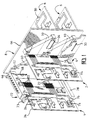
- interconnection system 2 interconnects circuit boards 4 with circuit boards 6. To insure that the interconnection has been effected, interconnection system 2 is provided with an interconnection member 8 which accurately positions circuit boards 4, 6 and provides the electrical connectors 10 required to insure that circuit boards 4 are in electrical engagement with circuit boards 6.
- circuit boards 4 are provided. These circuit boards are spaced from each other and extend essentially parallel to one another. The circuit boards 4 are essentially perpendicular to a first major surface 12 (Figure 1) of interconnection member 8.
- each circuit board 4 has circuitry 14 provided on at least one surface thereof.
- Conductive paths 16 cooperate with the circuitry 14 to provide the electrical paths required for operation.
- Conductive paths 16 extend from circuitry 14 to mating areas 18 of circuit board 4.
- Mating areas 18 extend from a leading edge 20 of circuit board 4.
- Conductive areas 22 are provided on the mating areas 18, the conductive areas 22 being in electrical engagement with respective conductive paths 16 of the circuit board 4.
- conductive paths 16 are provided in electrical engagement with conductive pads 24 which are located on the side edges 26 of each circuit board 4. These conductive pads 24 are provided to supply the power and ground signals required for the operation of circuit boards 4.
- circuit boards 4 are shown in the figures, any number of circuit boards 4 can be provided.
- circuit boards 6 are provided. These circuit boards are spaced from each other and extend essentially parallel to one another.
- the circuit boards 6 are essentially perpendicular to a first major surface 28 of interconnection member 8.
- Circuit boards 6 are also essentially perpendicular to circuit boards 4.
- each circuit board 6 has circuitry 30 provided on at least one surface thereof.
- Conductive paths 32 cooperate with the circuitry 30 to provide the electrical paths required for operation.
- Conductive paths 32 extend from circuitry 30 to mating areas 34 of circuit board 6.
- Mating areas 34 extend from a leading edge 36 of circuit board 6.
- Conductive areas 38 are provided on the mating areas 34, and are in electrical engagement with respective conductive paths 32 of the circuit board 6.
- conductive paths 32 are provided in electrical engagement with conductive pads 40 which are located on the side edges 42 of each circuit board 6. These conductive pads 40 are provided to supply the power and ground signals required for the operation of circuit boards 6.
- circuit boards 6 are shown in the figures, any number of circuit boards 6 can be provided.
- Interconnection member 8 As shown in Figure 1 and 2, circuit boards 4 and 6 are maintained in electrical engagement by means interconnection member 8.
- Interconnection member 8 as shown in Figure 4, has a first planar member 44 and a second planar member 46.
- First planar member 44 is spaced from and extends essentially parallel to second planar member 46.
- First major surface 12 of interconnection member 8 is provided on first planar member 44, and second major surface 28 is provided on second planar member 46.
- Openings 48, 50 are provided on, and extend through first and second planar members 44, 46. As is best shown in Figure 1, openings 48 are essentially perpendicular to openings 50, such that mating areas 18 of circuit boards 4 cooperate with openings 48 and mating areas 34 of circuit boards 6 cooperate with openings 50, as will be discussed. It should be noted that openings 48 of first planar member 44 are provided in alignment with respective openings 48 of second planar member 46. Similarly, openings 50 of first planar member 44 are positioned in alignment with openings 50 of second planar member 46.
- electrical connectors 10 are positioned between first planar member 44 and second planar member 46.
- Electrical connector 10 is essentially triangular in configuration and has a first major surface 52, a second major surface 54, and side surfaces 56, 58, 60 extending therebetween.
- Mounting holes 62 are provided proximate the corners of electrical connector 10, the mounting holes 62 extend from first major surface 52 to second major surface 54.
- the electrical connectors 10 are maintained in position with respect to first and second planar members 44, 46 by screws 63 or other securing means which cooperate with mounting holes 62. Screws extend through openings 61 of planar members 44, 46 and holes 62 to not only maintain connectors 10 in position, but to also maintain planar members 44, 46 is position with respect to each other.
- a flexible cable 64 is provided to cooperate with the electrical connector 10.
- One example of the type of cable 64 which can be used is described in U.S. Patent Number 4,453,309.
- individual conductors 66 are partially encased in an adhesive material 67, such that the conductors 66 are maintained in a spaced apart fashion. A portion of each conductor is exposed, as shown in Figure 5.
- the adhesive material 67 mechanically locks conductors 66 therein, while providing the nonrigid characteristics required to allow the cable 64 to be formed into any shape desired.
- Conductors 66 can be selected of a material with resilient spring properties, such that as the cable is formed, resilient spring energy is stored and utilized to apply pressure at the points of contact between conductors 66 and conductive areas 22, 38, as will be discussed.
- the flexible cable 64 is bent around the electrical connector 10.
- a first end 68 of the cable is positioned proximate side surface 56.
- the cable is then bent such that cable 64 extends along first major surface 52, around side surface 58, and along second major surface 54.
- a second end 70 of the cable is positioned proximate side surface 60.
- the cable is bent around electrical connector 10 in such a manner so that the portions of the wires which are encased by the adhesive material 67 are provided proximate the electrical connector 10, and the exposed portions of the conductors 66 are provided away from the electrical connector 10. This allows for the conductors to electrically engage boards 4, 6 when boards 4, 6 are provided in openings 48, 50, as will be discussed.
- Power is supplied to boards 4, 6 by way of power zero insertion force (ZIF) connector 72.
- ZIF zero insertion force
- the operation of these power ZIF connectors is essentially similar to that described in copending U.S. Patent Application Serial Number 127,747, filed December 2, 1987.
- the use of power ZIF connector 72 simplifies interconnection member 8.
- the conductive areas 22, 38 provided on the mating areas can all be used for signal transmission. Consequently, as interconnection member 8 is only used for signal transmission, the number of conductors 66 which are required for operation is minimized. This allows interconnection member 8 to be smaller, and allows the length of the conductors to be minimized, as the circuitry of the interconnection member is simplified.
- circuit boards 4 are placed in electrical connection with circuit boards 6 by means of interconnection member 8.
- Circuit boards 4 are inserted into channels 74 of connectors 72 and channels 76 of tracks 78.
- boards 4 are moved toward interconnection member 8. This movement continues until mating areas 18 cooperate with openings 48, and leading surface 20 engages first major surface 12.
- the alignment of mating areas 18 and openings 48 is insured due to the cooperation of channels 74, 76.
- channels 74, 76 are provided in alignment with openings 48 and act as a guide which insures that the mating areas 18 are aligned with openings 48.
- conductive areas 22 are placed in engagement with the exposed conductors 66 of cable 64. This engagement provides an electrical path across which the signal transmissions can travel. It should be noted, that due to the dense side-by-side spacing of conductors 66, multiple conductors 66 may engage a single conductive area 22, thereby providing for redundant, independent electrical connections.
- the resilient characteristics of conductors 66 insures that an electrical connection is insured between the conductors 66 and conductive areas 22 by providing a wiping action between conductive areas 22 and conductors 66 as boards 4 are inserted into openings 48.
- the resilient nature of conductors 66 also provides the characteristics required to allow for many cycles (insertions and removals) of the board without effecting the electrical characteristics thereof.
- conductive pads 40 are placed in alignment with terminals (not shown) of power connector 72.
- An actuator 73 is then engaged, causing the terminals to cooperate with the conductive pads 40 of board 4. This cooperation provides the electrical path required for current to flow from the terminals to boards 4. Also, the cooperation of the terminals with board 4 provides the means to maintain circuit board 4 is its inserted position.
- Interconnection system 2 is configured to insure for the reliable interconnection between circuit boards, in such a manner as to minimize the space required for such an interconnection, as well as minimizing the cost associated therewith. This type of configuration has several benefits associated therewith.
- Interconnection system 2 described above does not require the use of a mother board or backplane to interconnect the circuit boards 4, 6. This lowers the cost of the system, as the extra cost of a complex mother board is not required for operation.
- the use of individual connectors rather than a mother board also simplifies the signal paths required between circuit boards 4 and circuit boards 6.
- the signal paths, which are provided by the connectors and extend between respective circuit boards 4 and circuit boards 6, are short and direct. There is no need to extend the signal path in order to avoid other circuitry, as would be true in the case of a mother board. Consequently, the signal paths provided in interconnection system 2 are beneficial in all instances, but particularly when high speed applications are required.
Landscapes
- Coupling Device And Connection With Printed Circuit (AREA)
- Combinations Of Printed Boards (AREA)
- Mounting Of Printed Circuit Boards And The Like (AREA)
- Multi-Conductor Connections (AREA)
Claims (6)
- Elektrischer Verbinder (8), um eine Mehrzahl erster Schaltungskarten (4), versehen mit ersten leitfähigen Bereichen (18), mit einer Mehrzahl zweiter Schaltungskarten (6), versehen mit zweiten leitfähigen Bereichen (34), elektrisch zu verbinden, wobei der Verbinder (8) Haltermittel (44, 46) und auf den Haltermitteln (44, 46) angeordnete erste Positioniermittel (48) für das Zusammenwirken mit den ersten leitfähigen Bereichen (18) der ersten gedruckten Schaltungskarten (4) und zweite Positioniermittel (50) für das Zusammenwirken mit den zweiten leitfähigen Bereichen (34) der zweiten gedruckten Schaltungskarten (6) aufweist
und Verbindermittel (10) aufweist, die an den Haltermitteln (44, 46) angebracht sind und mit Leitern (66) versehen sind, wobei ein erstes Gegenführungsende (56) jedes Verbindermittels (10) unmittelbar an einem jeweiligen ersten Positioniermittel (48) bereitgestellt ist und ein zweites Gegenführungsende (60) jedes Verbindermittels (10) unmittelbar an einem jeweiligen zweiten Positioniermittel (50) bereitgestellt ist;
wobei beim Einführen einer ersten Schaltungskarte (4) in ein jeweiliges erstes Positioniermittel (48) die ersten leitfähigen Bereiche (18) der ersten Schaltungskarte (4) elektrisch in Verbindung mit den Leitern (66) an dem ersten Gegenführungsende (56) des Verbindermittels (10) gebracht werden, und beim Einführen einer zweiten Schaltungskarte (6) in ein jeweiliges zweites Positioniermittel (50) die zweiten leitfähigen Bereiche (34) der zweiten Schaltungskarte (6) in elektrische Verbindung mit den Leitern (66) an dem zweiten Gegenführungsende (60) des Verbindermittels (10) gebracht werden, wodurch die ersten Schaltungskarten (4) in elektrische Verbindung mit den zweiten Schaltungskarten (6) gebracht werden, dadurch gekennzeichnet, daß:
die Haltermittel zwei ebene, parallel voneinander räumlich getrennte Halter (44, 46) aufweisen, durchbrochen von zwei Sätzen gegenseitig orthogonaler länglicher Öffnungen (48, 50), die die Positioniermittel darstellen, die Verbindermittel (10) in dem Raum zwischen den Haltern (44,46) angeordnet sind und mit einem Flachkabel (64) versehen sind, bei dem freiliegende Leiterenden angrenzend an die Öffnungen (48, 50) angeordnet sind, und die leitfähigen Bereiche (18, 34) Randkontakte (22) aufweisen und durch jeweilige der Öffnungen (48, 50) einführbar sind, um elektrischen Kontakt zwischen den Randkontakten (22) und den freiliegenden Leiterenden des Flachkabels (64) herzustellen. - Elektrischer Verbinder (8) nach Anspruch 1, dadurch gekennzeichnet, daß die ebenen Halter (44, 46) Sicherungsmittel (61) für das Zusammenwirken mit den Verbindermitteln (10) haben, um den Abstand zwischen den ebenen Haltern (44, 46) aufrechtzuerhalten und um die Verbindermittel (10) in dem Raum dazwischen zu halten.
- Elektrischer Verbinder (8) nach Anspruch 1 oder 2, dadurch gekennzeichnet, daß die Öffnungen (48, 50) so dimensioniert sind, daß beim Einführen der jeweiligen ersten und zweiten leitfähigen Bereiche (18, 34) die Öffnungen (48, 50) mit den leitfähigen Bereichen (18, 34) zusammenwirken, um die leitfähigen Bereiche (18, 34) darin festzuhalten.
- Elektrischer Verbinder (8) nach Anspruch 1, 2 oder 3, dadurch gekennzeichnet, daß sich Führungsschienen (72, 78) für das Zusammenwirken mit den Seitenkanten der Schaltungskarten (4, 6) von den ebenen Haltern (44, 46) in eine hierzu im wesentlichen senkrechte Richtung erstrecken, um die Schaltungskarten (4, 6) zu führen, wenn die leitfähigen Bereiche (18, 34) in die Öffnungen (48, 50) eingeführt werden.
- Elektrischer Verbinder (8) nach Anspruch 4, dadurch gekennzeichnet, daß die Führungsschienen (72, 78) in elektrischer Verbindung mit den Leitern auf den Schaltungskarten (4, 6) stehen, so daß die Führungsschienen (72, 78) Energie- und Massepfade bereitstellen, die für den Betrieb der Schaltungskarten (4, 6) benötigt werden.
- System (2) zur Verbindung von Schaltungskarten (4, 6), wobei das System Folgendes aufweist:
eine Mehrzahl erster Schaltungskarten (4), wobei die ersten Schaltungskarten (4) räumlich voneinander getrennt sind und sich im wesentlichen parallel zueinander erstrecken, eine Mehrzahl zweiter Schaltungskarten (6), wobei die zweiten Schaltungskarten (6) räumlich voneinander getrennt sind und sich im wesentlichen parallel zueinander erstrecken und die zweiten Schaltungskarten (6) und die ersten Schaltungskarten (4) als orthogonales Feld zueinander angeordnet sind, eine Mehrzahl leitfähiger Bereiche (18, 34), die auf den ersten und zweiten Schaltungskarten (4, 6) bereitgestellt sind, und worin:
eine Mehrzahl Verbindermittel (10) unmittelbar bei den leitfähigen Bereichen (18, 34) der ersten Schaltungskarten (4) bereitgestellt ist, jedes jeweilige Verbindermittel in elektrischer Verbindung mit einem jeweiligen leitfähigen Bereich (18, 34) einer zweiten Schaltungskarte (6) steht, so daß ein elektrischer Pfad für Signale der ersten Schaltungskarte (4) und der zweiten Schaltungskarte (6) bereitgestellt ist, und das gekennzeichnet ist durch:
zwei parallel räumlich voneinander getrennte Halter (44, 46), durchbrochen von zwei Sätzen gegenseitig orthogonaler länglicher Öffnungen (48, 50), die Verbindermittel (10), die in dem Raum zwischen den Haltern (44, 46) angeordnet sind, mit einem Flachkabel (64) versehen sind, das freiliegende Leiterenden hat, die angrenzend an die Öffnungen (48, 50) angeordnet sind, und die leitfähigen Bereiche (18, 34) Randkontakte (22) aufweisen und sich durch jeweilige der Öffnungen (48, 50) in elektrischem Kontakt mit jeweiligen freiliegenden Leiterenden des Flachkabels (64) erstrecken.
Applications Claiming Priority (2)
| Application Number | Priority Date | Filing Date | Title |
|---|---|---|---|
| US207411 | 1988-06-15 | ||
| US07/207,411 US4838798A (en) | 1988-06-15 | 1988-06-15 | High density board to board interconnection system |
Publications (2)
| Publication Number | Publication Date |
|---|---|
| EP0347077A1 EP0347077A1 (de) | 1989-12-20 |
| EP0347077B1 true EP0347077B1 (de) | 1994-10-26 |
Family
ID=22770440
Family Applications (1)
| Application Number | Title | Priority Date | Filing Date |
|---|---|---|---|
| EP89305599A Expired - Lifetime EP0347077B1 (de) | 1988-06-15 | 1989-06-02 | Platte an Platte-Zusammenschaltungssystem mit hoher Kontaktdichte |
Country Status (4)
| Country | Link |
|---|---|
| US (1) | US4838798A (de) |
| EP (1) | EP0347077B1 (de) |
| JP (1) | JP2865312B2 (de) |
| DE (1) | DE68918992T2 (de) |
Families Citing this family (52)
| Publication number | Priority date | Publication date | Assignee | Title |
|---|---|---|---|---|
| US4907975A (en) * | 1988-12-19 | 1990-03-13 | International Business Machine Corporation | Electrical connector utilizing flexible electrical circuitry |
| US5093985A (en) * | 1989-06-30 | 1992-03-10 | John Houldsworth | Method of assembly for small electrical devices |
| US4971563A (en) * | 1989-07-27 | 1990-11-20 | Wells Iii William M | Modular backplane assemblies for computers |
| US5205739A (en) * | 1989-11-13 | 1993-04-27 | Augat Inc. | High density parallel interconnect |
| US5102342A (en) * | 1989-11-13 | 1992-04-07 | Augat Inc. | Modified high density backplane connector |
| US5037310A (en) * | 1989-12-06 | 1991-08-06 | Gespac, Inc. | Connector apparatus and method for distributed control modules used in computer networks |
| US5167511A (en) * | 1990-11-27 | 1992-12-01 | Cray Research, Inc. | High density interconnect apparatus |
| US5211565A (en) * | 1990-11-27 | 1993-05-18 | Cray Research, Inc. | High density interconnect apparatus |
| US5335146A (en) * | 1992-01-29 | 1994-08-02 | International Business Machines Corporation | High density packaging for device requiring large numbers of unique signals utilizing orthogonal plugging and zero insertion force connetors |
| US5321585A (en) * | 1992-06-25 | 1994-06-14 | General Motors Corporation | Directly solderable auxiliary circuit board assembly and methods of making and using the same |
| EP0581471A1 (de) * | 1992-07-29 | 1994-02-02 | Fujitsu Limited | Bildsteuerungsanlage |
| US5402078A (en) * | 1992-10-13 | 1995-03-28 | Micro Control Company | Interconnection system for burn-in boards |
| US5541586A (en) * | 1993-05-03 | 1996-07-30 | The Whitaker Corporation | Visual outlet identification in a cable management system |
| US5432505A (en) * | 1993-05-03 | 1995-07-11 | The Whitaker Corporation | Cable management system with automatic mapping |
| US5402320A (en) * | 1993-11-18 | 1995-03-28 | Northern Telecom Limited | Electronic shelf keying and alignment combination |
| EP0685906A1 (de) * | 1994-06-01 | 1995-12-06 | Saia Ag | Verfahren zur Herstellung eines Elektrogerätes und nach diesem Verfahren hergestelltes Elektrogerät |
| DE19502408A1 (de) * | 1995-01-26 | 1996-08-01 | Siemens Ag | Leiterplatten-Anschlußeinrichtung mit einer Vielzahl von elektrischen Kontaktierungsstellen in der Bestückungsebene der Leiterplatte |
| JP3543555B2 (ja) * | 1997-08-08 | 2004-07-14 | 株式会社日立製作所 | 信号伝送装置 |
| EP1016335B1 (de) * | 1997-09-15 | 2001-12-19 | Siemens Aktiengesellschaft | Elektrisches gerät mit einem justierelement |
| JP3698233B2 (ja) * | 1998-04-28 | 2005-09-21 | 富士通株式会社 | プリント配線板実装構造 |
| CA2296953A1 (en) * | 1999-01-28 | 2000-07-28 | Berg Technology, Inc. | Electrical connector mateable in a plurality of orientations |
| US6360435B1 (en) * | 1999-08-25 | 2002-03-26 | Qualcomm Incorporated | Bidirectional interface tool for PWB development |
| US6422876B1 (en) * | 1999-12-08 | 2002-07-23 | Nortel Networks Limited | High throughput interconnection system using orthogonal connectors |
| US6411520B1 (en) * | 2000-04-18 | 2002-06-25 | Grass Valley Group | Modular equipment frame and modules |
| US6533587B1 (en) * | 2000-07-05 | 2003-03-18 | Network Engines, Inc. | Circuit board riser |
| US6538899B1 (en) * | 2001-01-02 | 2003-03-25 | Juniper Networks, Inc. | Traceless midplane |
| US6568944B1 (en) * | 2001-02-21 | 2003-05-27 | Adc Telecommunications, Inc. | Circuit board with increased edge connection capacity |
| US6824393B2 (en) * | 2001-05-29 | 2004-11-30 | International Business Machines Corporation | Fragmented backplane system for I/O applications |
| US6717825B2 (en) * | 2002-01-18 | 2004-04-06 | Fci Americas Technology, Inc. | Electrical connection system for two printed circuit boards mounted on opposite sides of a mid-plane printed circuit board at angles to each other |
| US6824394B1 (en) * | 2003-07-01 | 2004-11-30 | Phionics, Inc. | Modular sensor systems with elastomeric connectors |
| US6918775B2 (en) * | 2003-09-23 | 2005-07-19 | Hon Hai Precision Ind. Co., Ltd. | Method for interconnecting multiple printed circuit boards |
| US6866518B1 (en) * | 2003-09-23 | 2005-03-15 | Hon Hai Precision Ind. Co., Ltd. | Electrical interconnection between multiple printed circuit boards |
| US20050068754A1 (en) * | 2003-09-25 | 2005-03-31 | International Business Machines Corporation | System and method for a self aligning multiple card enclosure with hot plug capability |
| US8185838B2 (en) * | 2003-11-03 | 2012-05-22 | Bomers Florian U | Universal computer input event translator |
| EP1726073A4 (de) * | 2003-11-28 | 2008-12-17 | Kenneth James Warburton | Überbrückter parallelverteilrahmen |
| TW200529497A (en) * | 2004-02-24 | 2005-09-01 | Hon Hai Prec Ind Co Ltd | Method for interconnecting multiple printed circuit boards |
| US8444436B1 (en) * | 2004-07-01 | 2013-05-21 | Amphenol Corporation | Midplane especially applicable to an orthogonal architecture electronic system |
| US7283374B2 (en) * | 2005-02-03 | 2007-10-16 | Fujitsu Limited | Grow as you go equipment shelf |
| US7625214B2 (en) * | 2005-09-21 | 2009-12-01 | Hewlett-Packard Development Company, L.P. | High density power connector with impedance control |
| US7239528B1 (en) * | 2005-10-05 | 2007-07-03 | Cisco Technology, Inc. | Techniques for accommodating variations in chassis tolerances |
| US7680927B2 (en) * | 2005-11-17 | 2010-03-16 | Bea Systems, Inc. | System and method for providing testing for a communities framework |
| US7298625B1 (en) * | 2007-01-17 | 2007-11-20 | Inventec Corporation | Expansion structure of memory module slot |
| US8118611B2 (en) * | 2008-10-31 | 2012-02-21 | Myoungsoo Jeon | PCB bridge connector for connecting PCB devices |
| US20110250767A1 (en) * | 2010-04-08 | 2011-10-13 | Alan Crighton | Electrical connector system having transition assembly |
| US8687350B2 (en) * | 2011-05-11 | 2014-04-01 | Ez-Tech Corp | Motherboard and case with hidden internal connectors |
| US9756756B2 (en) * | 2012-03-26 | 2017-09-05 | Lenovo (Singapore) Pte. Ltd. | Drive cage and wires |
| US9274548B2 (en) * | 2013-03-01 | 2016-03-01 | Seagate Technology Llc | Electronic apparatus comprising backplane and methods of assembling and disassembling |
| US10588236B2 (en) * | 2015-07-24 | 2020-03-10 | Transtector Systems, Inc. | Modular protection cabinet with flexible backplane |
| CN107770956A (zh) * | 2016-08-16 | 2018-03-06 | 光宝电子(广州)有限公司 | 电路板结构 |
| US20220368047A1 (en) * | 2022-07-26 | 2022-11-17 | Intel Corporation | Adapter card with compression attached memory modules |
| US20240206066A1 (en) * | 2022-12-20 | 2024-06-20 | Qualcomm Incorporated | Hybrid circuit board device to support circuit reuse and method of manufacture |
| US20240314930A1 (en) * | 2023-03-14 | 2024-09-19 | Samsung Electronics Co., Ltd. | Computing system with connecting boards |
Family Cites Families (22)
| Publication number | Priority date | Publication date | Assignee | Title |
|---|---|---|---|---|
| FR2278222A1 (fr) * | 1974-07-12 | 1976-02-06 | Socapex | Connecteur a enfichage sans frottement |
| US4164362A (en) * | 1977-03-11 | 1979-08-14 | Amp Incorporated | Modular card cage with multiple power bus bar means |
| US4134631A (en) * | 1977-09-13 | 1979-01-16 | Amp Incorporated | Modular plug board system |
| US4220382A (en) * | 1978-12-15 | 1980-09-02 | Amp Incorporated | Bussing connector |
| JPS55121284A (en) * | 1979-03-09 | 1980-09-18 | Shinetsu Polymer Co | Card etch type connector |
| US4337499A (en) * | 1980-11-03 | 1982-06-29 | Lockheed Corp | Electronic enclosure and articulated back panel for use therein |
| JPS5839888U (ja) * | 1981-09-11 | 1983-03-16 | パイロツトインキ株式会社 | フエルト状ペン体 |
| US4401351A (en) * | 1981-09-28 | 1983-08-30 | Advant Corporation | Expandable card cage |
| US4453309A (en) * | 1981-11-20 | 1984-06-12 | Amp Incorporated | Manufacture of dense, flat conductor connectors |
| US4511950A (en) * | 1983-06-27 | 1985-04-16 | Northern Telecom Limited | Backpanel assemblies |
| JPS6021201U (ja) * | 1983-07-21 | 1985-02-14 | 株式会社吉野工業所 | 髪染め用塗布容器 |
| US4498717A (en) * | 1983-08-29 | 1985-02-12 | Gte Communication Systems Corp. | Printed wiring board interconnect arrangement |
| US4552420A (en) * | 1983-12-02 | 1985-11-12 | E. I. Du Pont De Nemours And Company | Electrical connector using a flexible circuit having an impedance control arrangement thereon |
| WO1986004208A1 (fr) * | 1984-12-28 | 1986-07-17 | Micro Engineering Co., Ltd. | Procede d'empilage de cartes de circuits imprimes |
| US4603928A (en) * | 1985-03-20 | 1986-08-05 | Amp Incorporated | Board to board edge connector |
| US4614389A (en) * | 1985-06-17 | 1986-09-30 | At&T Bell Laboratories | Circuit board assembly for accurate insertion |
| FR2589286B1 (fr) * | 1985-10-25 | 1988-05-13 | Cit Alcatel | Ensemble d'interconnexion de cartes de circuits imprimes orthogonales et reseaux de commutation en faisant application |
| US4693529A (en) * | 1986-03-31 | 1987-09-15 | Amp Incorporated | Elastomeric mother-daughter board electrical connector |
| US4708660A (en) * | 1986-06-23 | 1987-11-24 | Control Data Corporation | Connector for orthogonally mounting circuit boards |
| EP0272008B1 (de) * | 1986-12-19 | 1994-06-01 | The Whitaker Corporation | Modularer Verteilungsverbinder für Schaltkarte |
| JPH01135002U (de) * | 1988-03-10 | 1989-09-14 | ||
| JPH01164904U (de) * | 1988-05-10 | 1989-11-17 |
-
1988
- 1988-06-15 US US07/207,411 patent/US4838798A/en not_active Expired - Fee Related
-
1989
- 1989-06-02 DE DE68918992T patent/DE68918992T2/de not_active Expired - Fee Related
- 1989-06-02 EP EP89305599A patent/EP0347077B1/de not_active Expired - Lifetime
- 1989-06-05 JP JP1142878A patent/JP2865312B2/ja not_active Expired - Lifetime
Also Published As
| Publication number | Publication date |
|---|---|
| EP0347077A1 (de) | 1989-12-20 |
| DE68918992T2 (de) | 1995-06-01 |
| DE68918992D1 (de) | 1994-12-01 |
| JPH0236595A (ja) | 1990-02-06 |
| US4838798A (en) | 1989-06-13 |
| JP2865312B2 (ja) | 1999-03-08 |
Similar Documents
| Publication | Publication Date | Title |
|---|---|---|
| EP0347077B1 (de) | Platte an Platte-Zusammenschaltungssystem mit hoher Kontaktdichte | |
| EP0554077B1 (de) | Montageanordnung | |
| US4331370A (en) | Connection system for printed circuit boards | |
| US4705332A (en) | High density, controlled impedance connectors | |
| US5951320A (en) | Electrical interconnect system with wire receiving portion | |
| US6494734B1 (en) | High density electrical connector assembly | |
| EP1087300B1 (de) | Computerbusschienenanordnung | |
| RU2013897C1 (ru) | Электронная система | |
| US5980321A (en) | High speed, high density electrical connector | |
| KR100639560B1 (ko) | 차동 신호 전기 커넥터용 인쇄회로기판 | |
| EP1382094B1 (de) | Elektrische verbinderbaugruppe zur orthogonalen verbindung von leiterplatten | |
| US3660803A (en) | Electrical connectors | |
| EP0107288B1 (de) | Elektrischer Verbinderzusammenbau zum Anschliessen eines elektrischen abgeschirmten Flachkabels | |
| US6347039B1 (en) | Memory module and memory module socket | |
| EP0337634A1 (de) | Bezugsleitung zur Verbesserung der Integrität der Signale in elektrischen Steckverbindern | |
| US6866518B1 (en) | Electrical interconnection between multiple printed circuit boards | |
| US20020098721A1 (en) | Shielded carrier for land grid array connectors and a process for fabricating same | |
| EP0212764A2 (de) | Impedanz-kontrollierter Verbinder mit hoher Packungsdichte | |
| US5928036A (en) | Dual row memory card connector | |
| WO1994003942A1 (en) | Circuit interconnect system | |
| US6918775B2 (en) | Method for interconnecting multiple printed circuit boards | |
| JPH06223895A (ja) | コネクタおよびその方法 | |
| US4834660A (en) | Flexible zero insertion force interconnector between circuit boards | |
| US3368115A (en) | Modular housing for integrated circuit structure with improved interconnection means | |
| CA1124406A (en) | Circuit board and card interconnection system |
Legal Events
| Date | Code | Title | Description |
|---|---|---|---|
| PUAI | Public reference made under article 153(3) epc to a published international application that has entered the european phase |
Free format text: ORIGINAL CODE: 0009012 |
|
| AK | Designated contracting states |
Kind code of ref document: A1 Designated state(s): DE FR GB IT |
|
| 17P | Request for examination filed |
Effective date: 19900608 |
|
| 17Q | First examination report despatched |
Effective date: 19921112 |
|
| RAP1 | Party data changed (applicant data changed or rights of an application transferred) |
Owner name: THE WHITAKER CORPORATION |
|
| GRAA | (expected) grant |
Free format text: ORIGINAL CODE: 0009210 |
|
| AK | Designated contracting states |
Kind code of ref document: B1 Designated state(s): DE FR GB IT |
|
| REF | Corresponds to: |
Ref document number: 68918992 Country of ref document: DE Date of ref document: 19941201 |
|
| ITF | It: translation for a ep patent filed | ||
| ET | Fr: translation filed | ||
| PLBE | No opposition filed within time limit |
Free format text: ORIGINAL CODE: 0009261 |
|
| STAA | Information on the status of an ep patent application or granted ep patent |
Free format text: STATUS: NO OPPOSITION FILED WITHIN TIME LIMIT |
|
| 26N | No opposition filed | ||
| PGFP | Annual fee paid to national office [announced via postgrant information from national office to epo] |
Ref country code: GB Payment date: 19970506 Year of fee payment: 9 |
|
| PGFP | Annual fee paid to national office [announced via postgrant information from national office to epo] |
Ref country code: FR Payment date: 19970610 Year of fee payment: 9 |
|
| PGFP | Annual fee paid to national office [announced via postgrant information from national office to epo] |
Ref country code: DE Payment date: 19970627 Year of fee payment: 9 |
|
| PG25 | Lapsed in a contracting state [announced via postgrant information from national office to epo] |
Ref country code: GB Free format text: LAPSE BECAUSE OF NON-PAYMENT OF DUE FEES Effective date: 19980602 |
|
| GBPC | Gb: european patent ceased through non-payment of renewal fee |
Effective date: 19980602 |
|
| PG25 | Lapsed in a contracting state [announced via postgrant information from national office to epo] |
Ref country code: FR Free format text: LAPSE BECAUSE OF NON-PAYMENT OF DUE FEES Effective date: 19990226 |
|
| PG25 | Lapsed in a contracting state [announced via postgrant information from national office to epo] |
Ref country code: DE Free format text: LAPSE BECAUSE OF NON-PAYMENT OF DUE FEES Effective date: 19990401 |
|
| REG | Reference to a national code |
Ref country code: FR Ref legal event code: ST |
|
| PG25 | Lapsed in a contracting state [announced via postgrant information from national office to epo] |
Ref country code: IT Free format text: LAPSE BECAUSE OF NON-PAYMENT OF DUE FEES;WARNING: LAPSES OF ITALIAN PATENTS WITH EFFECTIVE DATE BEFORE 2007 MAY HAVE OCCURRED AT ANY TIME BEFORE 2007. THE CORRECT EFFECTIVE DATE MAY BE DIFFERENT FROM THE ONE RECORDED. Effective date: 20050602 |