EP0346800B1 - Filtre séparateur numérique - Google Patents
Filtre séparateur numérique Download PDFInfo
- Publication number
- EP0346800B1 EP0346800B1 EP89110601A EP89110601A EP0346800B1 EP 0346800 B1 EP0346800 B1 EP 0346800B1 EP 89110601 A EP89110601 A EP 89110601A EP 89110601 A EP89110601 A EP 89110601A EP 0346800 B1 EP0346800 B1 EP 0346800B1
- Authority
- EP
- European Patent Office
- Prior art keywords
- filter
- digital
- signal
- fir
- filters
- Prior art date
- Legal status (The legal status is an assumption and is not a legal conclusion. Google has not performed a legal analysis and makes no representation as to the accuracy of the status listed.)
- Expired - Lifetime
Links
- 238000000926 separation method Methods 0.000 title claims abstract description 15
- 239000013598 vector Substances 0.000 description 9
- 230000005540 biological transmission Effects 0.000 description 2
- 238000011045 prefiltration Methods 0.000 description 2
- 238000005070 sampling Methods 0.000 description 2
- 230000003111 delayed effect Effects 0.000 description 1
- 238000010586 diagram Methods 0.000 description 1
- 238000000034 method Methods 0.000 description 1
- 230000010355 oscillation Effects 0.000 description 1
- 230000003595 spectral effect Effects 0.000 description 1
Images
Classifications
-
- H—ELECTRICITY
- H03—ELECTRONIC CIRCUITRY
- H03H—IMPEDANCE NETWORKS, e.g. RESONANT CIRCUITS; RESONATORS
- H03H17/00—Networks using digital techniques
- H03H17/02—Frequency selective networks
- H03H17/06—Non-recursive filters
-
- H—ELECTRICITY
- H04—ELECTRIC COMMUNICATION TECHNIQUE
- H04L—TRANSMISSION OF DIGITAL INFORMATION, e.g. TELEGRAPHIC COMMUNICATION
- H04L27/00—Modulated-carrier systems
- H04L27/10—Frequency-modulated carrier systems, i.e. using frequency-shift keying
- H04L27/14—Demodulator circuits; Receiver circuits
Definitions
- the invention relates to a digital filter filter according to the preamble of patent claim 1.
- the invention describes a digital implementation of an FSK (Frequency Shift Keying) data receiver for demodulating frequency shift keyed data signals.
- FSK Frequency Shift Keying
- the direct current-free transmission of digital data over long distances is generally carried out with the aid of FSK modulation, whereby - for the duration of a bit to be transmitted - the logical state of the "0" oscillation trains of the separation frequency position (space frequency), that of the logical "1" Wave trains of the symbol frequency position (mark frequency) are sent.
- the arrangement of a data receiver described here serves to convert a frequency-shift-keyed data signal back into the baseband, ie to recover the digital information contained in it.
- a frequency-shift-keyed data signal is first pre-filtered in an analog manner (anti-aliasing low-pass filter) and converted analog / digital. Then the (now digitized) FSK signal in a pre-filter BPv (digital bandpass) is roughly from Noise and adjacent channel interference are eliminated.
- the band-filtered FSK signal x (n) then branches into two digital separation bank passes BP_mark and BP_space which are arranged parallel to one another.
- One separation band pass (BP_space) is tuned to the separation frequency, the other separation band pass (BP_mark) to the symbol frequency.
- the output signals y1 (n) and y2 (n) of both separation bandpasses are squared.
- the FSK signal is not demodulated by rectification, but by squaring in order to avoid uncorrectable distortions caused by spectral components beyond half the sampling frequency.
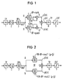
- the invention has for its object to provide ways to simplify the signal flow graph of the digital filter filter according to FIG. 1 and thereby to come to simpler circuits.
- the path A there is a bandpass filter 4 with the coefficient vector a , which is tuned to the symbol frequency, so that the signal y1 (n) emerges from the bandpass filter 4.
- This signal is squared in a squarer 6, which is indicated by the fact that the signal y1 (n) is fed to the 2 inputs of the squarer 6.
- the squared output signal y3 (n) is fed to the summer 7.
- the bandpass 5 with the coefficient vector b which is tuned to the crossover frequency, is first run through in path B.
- the output signal y2 (n) is fed to a squarer 6 ', which is also indicated in such a way that the output signal y2 (n) is fed to both inputs of the squarer 6'.
- the output signal of the squarer 6 ' is designated y4 (n). This output signal is fed to the summer 7 inverted.
- the signal x (n) is again split into paths A and B.
- a path 10 is provided in path A, the output signal of which is designated y5 (n).
- a bandpass filter 11 is provided in path B, the output signal of which is designated y6 (n).
- These two output signals are combined in a multiplier 12, the output signal of which in turn passes through the low-pass filter 8 and the decider 9. It is essential that the bandpasses 10 and 11 are designed as transversal filters and that transversal bandpasses 4 and 5 are assumed.
- the bandpasses 10 and 11 are dimensioned such that their coefficients result from the sum ( a + b ) or from the difference ( a - b ) of the coefficients of the original transverse bandpasses 4 and 5. This is indicated by the note FIR BP_modl or pointing FIR BP_mod2, reference being made to the transversal filter ( "F init I mpulse R esponse” filter).
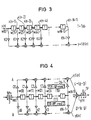
- FIG. 3 shows the signal flow graph for a transversal filter of degree N.
- the input signal x (n) runs through a delay chain with the delay elements T.
- the individual delayed input values (for example x (n-4)) are also identified, as are the corresponding ones State variables, for example w (0) and w (4). Accordingly, the individual filter coefficients are designated k0 ..., k4 ..., kN-1.
- the signals are summed up in adders (+) and are available at the output as signal y_FIR (n).
- FIG. 2 The explanation given for FIG. 2 can be used directly for the signal flow graph of FIG. 4.
- the state variables w (0) to w (N-1) can be seen, the filter coefficients c0 to cN-1 in path A and the filter coefficients d0 to dN-1 in path B.
- Those in paths A and B respectively in the Totalizers (+) Accumulated signals y5 (n) and y6 (n) are combined at multiplier 12 and are available at the output of low-pass filter 8.
- the signal flow graph of the digital filter filter according to FIG. 1 can be further simplified under certain conditions: If both separation bandpasses BP_mark and BP_space FIR filters are of degree N, as shown in FIG. 2, squaring and subsequent subtraction can be attributed to a ONLY multiplication. In addition, only ONE common state memory w is required for BOTH separation bandpasses.
- FIG. 3 shows the signal flow graph for a FIR filter of degree N.
- Such transverse filter structures can be implemented particularly easily, for example, in a digital signal processor.
- the preselected input signal x (n) to be demodulated is simultaneously fed to the two "modified" digital FIR separation bandpasses BP_mod1 and BP_mod2.
Landscapes
- Engineering & Computer Science (AREA)
- Physics & Mathematics (AREA)
- Computer Hardware Design (AREA)
- Mathematical Physics (AREA)
- Computer Networks & Wireless Communication (AREA)
- Signal Processing (AREA)
- Digital Transmission Methods That Use Modulated Carrier Waves (AREA)
- Image Processing (AREA)
- Complex Calculations (AREA)
- Oscillators With Electromechanical Resonators (AREA)
- Networks Using Active Elements (AREA)
- Filters That Use Time-Delay Elements (AREA)
Claims (2)
- Filtre séparateur numérique, notamment pour un récepteur de données, qui comporte un convertisseur analogique/numérique (2) et dans lequel les signaux numériques sont répartis, en aval du convertisseur analogique/numérique (2) et d'un préfiltre (3), entre une première voie (A) et une seconde voie (B), par des filtres passe-bande numériques (4,5) associés de façon correspondante, caractérisé par le fait
que les deux filtres passe-bande (4,5) sont agencés sous la forme de filtres transversaux (10,11), et
que ces filtres transversaux (10,11) sont dimensionnés de telle sorte que leurs coefficients sont déterminés à partir de la somme ou de la différence des coefficients des deux filtres passe-bande transversaux (4,5), et que les deux voies (A,B) sont interconnectées par l'intermédiaire d'un multiplicateur (12). - Filtre séparateur numérique suivant la revendication 1, caractérisé par le fait que pour les deux filtres passe-bande transversaux (10,11), il n'est prévu qu'une mémoire d'état commune (w, chaîne de retardement).
Priority Applications (1)
| Application Number | Priority Date | Filing Date | Title |
|---|---|---|---|
| AT89110601T ATE101308T1 (de) | 1988-06-15 | 1989-06-12 | Digitale filterweiche. |
Applications Claiming Priority (2)
| Application Number | Priority Date | Filing Date | Title |
|---|---|---|---|
| DE3820386 | 1988-06-15 | ||
| DE3820386 | 1988-06-15 |
Publications (2)
| Publication Number | Publication Date |
|---|---|
| EP0346800A1 EP0346800A1 (fr) | 1989-12-20 |
| EP0346800B1 true EP0346800B1 (fr) | 1994-02-02 |
Family
ID=6356619
Family Applications (1)
| Application Number | Title | Priority Date | Filing Date |
|---|---|---|---|
| EP89110601A Expired - Lifetime EP0346800B1 (fr) | 1988-06-15 | 1989-06-12 | Filtre séparateur numérique |
Country Status (3)
| Country | Link |
|---|---|
| EP (1) | EP0346800B1 (fr) |
| AT (1) | ATE101308T1 (fr) |
| DE (1) | DE58906868D1 (fr) |
Family Cites Families (1)
| Publication number | Priority date | Publication date | Assignee | Title |
|---|---|---|---|---|
| ATE56573T1 (de) * | 1985-07-03 | 1990-09-15 | Siemens Ag | Digitale filterweiche, insbesondere fuer einen datenempfaenger. |
-
1989
- 1989-06-12 EP EP89110601A patent/EP0346800B1/fr not_active Expired - Lifetime
- 1989-06-12 AT AT89110601T patent/ATE101308T1/de not_active IP Right Cessation
- 1989-06-12 DE DE89110601T patent/DE58906868D1/de not_active Expired - Fee Related
Also Published As
| Publication number | Publication date |
|---|---|
| EP0346800A1 (fr) | 1989-12-20 |
| DE58906868D1 (de) | 1994-03-17 |
| ATE101308T1 (de) | 1994-02-15 |
Similar Documents
| Publication | Publication Date | Title |
|---|---|---|
| EP0208982B1 (fr) | Filtre numérique de dérivation pour un récepteur de données | |
| DE4326843C2 (de) | Empfangsverfahren und Empfangsantennensystem zur Beseitigung von Mehrwegstörungen bzw. Steuergerät zur Durchführung dieses Verfahrens | |
| DE2721850A1 (de) | Filter- und demodulationsanordnung | |
| DE69212214T2 (de) | Zeitdiskreter Stereo-Decoder | |
| EP0201758A2 (fr) | Démodulateur numérique pour signaux modulés en fréquence | |
| DE2334807A1 (de) | Verfahren und geraet zur ermittlung des mehrfachempfangs von frequenz-modulierten rundfunk-stereowellen ("geisterempfang" bei ukw-stereo-rundfunk) | |
| EP0346800B1 (fr) | Filtre séparateur numérique | |
| EP1657917B1 (fr) | Procédé et montage de circuit pour le filtrage de canal de signaux TV à modulation analogique ou numérique | |
| DE4419428A1 (de) | Schaltungsanordnung für einen Demodulator eines Radio-Daten-Signals in einem Rundfunkempfänger | |
| DE3750324T2 (de) | Vereinfachte Zurückgewinnung von Daten aus Signalen mit Quadraturträgern. | |
| DE69737875T2 (de) | Demodulationsvorrichtung für datenmodulierte Träger | |
| EP0123278B1 (fr) | Filtre numérique d'ondes réalisé par des filtres numériques d'ondes en pont | |
| DE19960559A1 (de) | Empfangsvorrichtung für winkelmodulierte Signale | |
| EP0268842A1 (fr) | Egaliseur adaptatif en bande passante pour systèmes numériques à faisceaux hertziens | |
| EP0080020B1 (fr) | Procédé pour la détermination des instants d'échantillonnage d'un signal reçu en modulation de quadrature de phase manipulée ou en modulation de quadrature d'amplitude | |
| DE69110491T2 (de) | FM-Demodulator. | |
| EP0642714B1 (fr) | Recepteur radio a traitement numerique de signaux | |
| DE3505950C2 (fr) | ||
| DE69937018T2 (de) | RDS Demodulator für den Empfang von Rundfunkprogrammen die Radiodatensignalen und Autofahrer Rundfunkinformationsignalen (ARI) enthalten, mit einer digitalen Filtervorrichtung die eine hohe Dämpfung des ARI Signals bewirkt | |
| EP0387245B1 (fr) | Element de circuit numerique de decodage dqpsk | |
| EP0179393A1 (fr) | Egaliseur transversal de fréquence intermédiaire | |
| EP0602435B1 (fr) | Méthode de démodulation pour des signaux modulés en fréquence | |
| DE3006801C2 (de) | Empfänger | |
| Glas | A differential FM detector for low-IF radios | |
| DE3246145A1 (de) | Fernsehuebertragungssystem mit integrierter uebertragung von zusatzinformationen, insbesondere tonsignalen |
Legal Events
| Date | Code | Title | Description |
|---|---|---|---|
| PUAI | Public reference made under article 153(3) epc to a published international application that has entered the european phase |
Free format text: ORIGINAL CODE: 0009012 |
|
| AK | Designated contracting states |
Kind code of ref document: A1 Designated state(s): AT BE DE FR GB IT LU NL SE |
|
| 17P | Request for examination filed |
Effective date: 19900528 |
|
| 17Q | First examination report despatched |
Effective date: 19920520 |
|
| GRAA | (expected) grant |
Free format text: ORIGINAL CODE: 0009210 |
|
| AK | Designated contracting states |
Kind code of ref document: B1 Designated state(s): AT BE DE FR GB IT LU NL SE |
|
| REF | Corresponds to: |
Ref document number: 101308 Country of ref document: AT Date of ref document: 19940215 Kind code of ref document: T |
|
| REF | Corresponds to: |
Ref document number: 58906868 Country of ref document: DE Date of ref document: 19940317 |
|
| ITF | It: translation for a ep patent filed | ||
| GBT | Gb: translation of ep patent filed (gb section 77(6)(a)/1977) |
Effective date: 19940412 |
|
| ET | Fr: translation filed | ||
| EPTA | Lu: last paid annual fee | ||
| PLBE | No opposition filed within time limit |
Free format text: ORIGINAL CODE: 0009261 |
|
| STAA | Information on the status of an ep patent application or granted ep patent |
Free format text: STATUS: NO OPPOSITION FILED WITHIN TIME LIMIT |
|
| 26N | No opposition filed | ||
| EAL | Se: european patent in force in sweden |
Ref document number: 89110601.5 |
|
| PGFP | Annual fee paid to national office [announced via postgrant information from national office to epo] |
Ref country code: AT Payment date: 19960530 Year of fee payment: 8 |
|
| PGFP | Annual fee paid to national office [announced via postgrant information from national office to epo] |
Ref country code: LU Payment date: 19960601 Year of fee payment: 8 |
|
| PGFP | Annual fee paid to national office [announced via postgrant information from national office to epo] |
Ref country code: BE Payment date: 19960612 Year of fee payment: 8 |
|
| PGFP | Annual fee paid to national office [announced via postgrant information from national office to epo] |
Ref country code: SE Payment date: 19960619 Year of fee payment: 8 |
|
| PGFP | Annual fee paid to national office [announced via postgrant information from national office to epo] |
Ref country code: NL Payment date: 19960620 Year of fee payment: 8 |
|
| PG25 | Lapsed in a contracting state [announced via postgrant information from national office to epo] |
Ref country code: LU Free format text: LAPSE BECAUSE OF NON-PAYMENT OF DUE FEES Effective date: 19970612 Ref country code: AT Effective date: 19970612 |
|
| PG25 | Lapsed in a contracting state [announced via postgrant information from national office to epo] |
Ref country code: SE Effective date: 19970613 |
|
| PG25 | Lapsed in a contracting state [announced via postgrant information from national office to epo] |
Ref country code: BE Effective date: 19970630 |
|
| BERE | Be: lapsed |
Owner name: SIEMENS A.G. Effective date: 19970630 |
|
| PG25 | Lapsed in a contracting state [announced via postgrant information from national office to epo] |
Ref country code: NL Effective date: 19980101 |
|
| EUG | Se: european patent has lapsed |
Ref document number: 89110601.5 |
|
| NLV4 | Nl: lapsed or anulled due to non-payment of the annual fee |
Effective date: 19980101 |
|
| PGFP | Annual fee paid to national office [announced via postgrant information from national office to epo] |
Ref country code: GB Payment date: 19980511 Year of fee payment: 10 |
|
| PGFP | Annual fee paid to national office [announced via postgrant information from national office to epo] |
Ref country code: FR Payment date: 19980624 Year of fee payment: 10 |
|
| PGFP | Annual fee paid to national office [announced via postgrant information from national office to epo] |
Ref country code: DE Payment date: 19980819 Year of fee payment: 10 |
|
| PG25 | Lapsed in a contracting state [announced via postgrant information from national office to epo] |
Ref country code: GB Free format text: LAPSE BECAUSE OF NON-PAYMENT OF DUE FEES Effective date: 19990612 |
|
| PG25 | Lapsed in a contracting state [announced via postgrant information from national office to epo] |
Ref country code: FR Free format text: THE PATENT HAS BEEN ANNULLED BY A DECISION OF A NATIONAL AUTHORITY Effective date: 19990630 |
|
| GBPC | Gb: european patent ceased through non-payment of renewal fee |
Effective date: 19990612 |
|
| PG25 | Lapsed in a contracting state [announced via postgrant information from national office to epo] |
Ref country code: DE Free format text: LAPSE BECAUSE OF NON-PAYMENT OF DUE FEES Effective date: 20000503 |
|
| REG | Reference to a national code |
Ref country code: FR Ref legal event code: ST |
|
| PG25 | Lapsed in a contracting state [announced via postgrant information from national office to epo] |
Ref country code: IT Free format text: LAPSE BECAUSE OF NON-PAYMENT OF DUE FEES;WARNING: LAPSES OF ITALIAN PATENTS WITH EFFECTIVE DATE BEFORE 2007 MAY HAVE OCCURRED AT ANY TIME BEFORE 2007. THE CORRECT EFFECTIVE DATE MAY BE DIFFERENT FROM THE ONE RECORDED. Effective date: 20050612 |