EP0344075A1 - Herstellungsüberwachung einer gedruckten Schaltung - Google Patents
Herstellungsüberwachung einer gedruckten Schaltung Download PDFInfo
- Publication number
- EP0344075A1 EP0344075A1 EP89420113A EP89420113A EP0344075A1 EP 0344075 A1 EP0344075 A1 EP 0344075A1 EP 89420113 A EP89420113 A EP 89420113A EP 89420113 A EP89420113 A EP 89420113A EP 0344075 A1 EP0344075 A1 EP 0344075A1
- Authority
- EP
- European Patent Office
- Prior art keywords
- circuit
- pads
- conductive
- studs
- checked
- Prior art date
- Legal status (The legal status is an assumption and is not a legal conclusion. Google has not performed a legal analysis and makes no representation as to the accuracy of the status listed.)
- Withdrawn
Links
- 238000004519 manufacturing process Methods 0.000 title claims abstract description 6
- 238000001514 detection method Methods 0.000 claims abstract description 8
- 239000000523 sample Substances 0.000 claims description 11
- 238000000034 method Methods 0.000 claims description 10
- 239000011810 insulating material Substances 0.000 claims description 5
- 238000011960 computer-aided design Methods 0.000 claims description 4
- 238000005259 measurement Methods 0.000 claims description 2
- 238000012795 verification Methods 0.000 claims description 2
- 238000002513 implantation Methods 0.000 claims 1
- 238000009413 insulation Methods 0.000 claims 1
- 238000011017 operating method Methods 0.000 claims 1
- 238000012360 testing method Methods 0.000 description 4
- 239000002184 metal Substances 0.000 description 3
- 230000002950 deficient Effects 0.000 description 1
- 230000006870 function Effects 0.000 description 1
- 230000000977 initiatory effect Effects 0.000 description 1
- 238000003908 quality control method Methods 0.000 description 1
- 238000012546 transfer Methods 0.000 description 1
Images
Classifications
-
- G—PHYSICS
- G01—MEASURING; TESTING
- G01R—MEASURING ELECTRIC VARIABLES; MEASURING MAGNETIC VARIABLES
- G01R31/00—Arrangements for testing electric properties; Arrangements for locating electric faults; Arrangements for electrical testing characterised by what is being tested not provided for elsewhere
- G01R31/28—Testing of electronic circuits, e.g. by signal tracer
- G01R31/2801—Testing of printed circuits, backplanes, motherboards, hybrid circuits or carriers for multichip packages [MCP]
- G01R31/2805—Bare printed circuit boards
Definitions
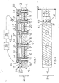
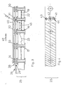
- the probe circuit 26 is specific, in the sense that it corresponds to the type of circuit 24, 25 to be tested. The user must, for each type of circuit printed to be tested, have the corresponding probe circuit 26.
- This probe circuit 26 constitutes the specific interface between the type of circuit 24, 25 to be tested, and the probe or auscultator apparatus 35 to 39 which, for its part, remains standard in all cases.
- the standard data for a circuit deemed to be "GOOD" can be entered into memory 39 according to any known method. For example, they may be parameters previously read on a standard circuit. It may also be data directly supplied by CAD ("computer-aided design").
Landscapes
- Engineering & Computer Science (AREA)
- Computer Hardware Design (AREA)
- Microelectronics & Electronic Packaging (AREA)
- General Engineering & Computer Science (AREA)
- Physics & Mathematics (AREA)
- General Physics & Mathematics (AREA)
- Testing Of Short-Circuits, Discontinuities, Leakage, Or Incorrect Line Connections (AREA)
- Tests Of Electronic Circuits (AREA)
Applications Claiming Priority (2)
| Application Number | Priority Date | Filing Date | Title |
|---|---|---|---|
| FR8804725A FR2629669B1 (fr) | 1988-03-30 | 1988-03-30 | Procede et dispositif pour la verification et le controle en fabrication d'un circuit imprime |
| FR8804725 | 1988-03-30 |
Publications (1)
| Publication Number | Publication Date |
|---|---|
| EP0344075A1 true EP0344075A1 (de) | 1989-11-29 |
Family
ID=9365150
Family Applications (1)
| Application Number | Title | Priority Date | Filing Date |
|---|---|---|---|
| EP89420113A Withdrawn EP0344075A1 (de) | 1988-03-30 | 1989-03-29 | Herstellungsüberwachung einer gedruckten Schaltung |
Country Status (4)
| Country | Link |
|---|---|
| EP (1) | EP0344075A1 (de) |
| JP (1) | JPH02504449A (de) |
| FR (1) | FR2629669B1 (de) |
| WO (1) | WO1989009535A1 (de) |
Citations (3)
| Publication number | Priority date | Publication date | Assignee | Title |
|---|---|---|---|---|
| FR2498335A1 (fr) * | 1981-01-19 | 1982-07-23 | Everett Charles Test Equipment | Appareil d'essai de plaquettes de circuit imprime muni d'une platine adaptable |
| DE3104227A1 (de) * | 1981-02-06 | 1982-08-19 | atg electronic GmbH, 6980 Wertheim | "leiterplattenpruefeinrichtung" |
| FR2590439A1 (fr) * | 1985-11-19 | 1987-05-22 | Teradyne Inc | Ensemble de broches d'essais perfectionne pour controleur de cartes ou plaquettes de circuits imprimes |
-
1988
- 1988-03-30 FR FR8804725A patent/FR2629669B1/fr not_active Expired - Lifetime
-
1989
- 1989-03-29 EP EP89420113A patent/EP0344075A1/de not_active Withdrawn
- 1989-03-29 WO PCT/FR1989/000147 patent/WO1989009535A1/fr not_active Ceased
- 1989-03-29 JP JP1504143A patent/JPH02504449A/ja active Pending
Patent Citations (3)
| Publication number | Priority date | Publication date | Assignee | Title |
|---|---|---|---|---|
| FR2498335A1 (fr) * | 1981-01-19 | 1982-07-23 | Everett Charles Test Equipment | Appareil d'essai de plaquettes de circuit imprime muni d'une platine adaptable |
| DE3104227A1 (de) * | 1981-02-06 | 1982-08-19 | atg electronic GmbH, 6980 Wertheim | "leiterplattenpruefeinrichtung" |
| FR2590439A1 (fr) * | 1985-11-19 | 1987-05-22 | Teradyne Inc | Ensemble de broches d'essais perfectionne pour controleur de cartes ou plaquettes de circuits imprimes |
Also Published As
| Publication number | Publication date |
|---|---|
| WO1989009535A1 (fr) | 1989-10-05 |
| FR2629669A1 (fr) | 1989-10-06 |
| JPH02504449A (ja) | 1990-12-13 |
| FR2629669B1 (fr) | 1991-05-17 |
Similar Documents
| Publication | Publication Date | Title |
|---|---|---|
| EP0518789B1 (de) | Nadelkarte für Chiptestgeräte | |
| FR2964193A1 (fr) | Procede de mesure d'une energie d'adhesion, et substrats associes | |
| FR2708106A1 (fr) | Douille d'essais et procédé de production de microplaquettes reconnues bonnes en utilisant cette douille. | |
| EP0410910A1 (de) | Membran-Deformationsmessvorrichtung | |
| EP0344075A1 (de) | Herstellungsüberwachung einer gedruckten Schaltung | |
| EP0030889B1 (de) | Verfahren und Vorrichtung zum zerstörungsfreien Prüfen von Punktschweissungen | |
| EP0581703B1 (de) | Verfahren zur Prüfung des Schichtwiderstandes einer Diffusionsschicht | |
| EP0147245B1 (de) | Vorrichtung und Verfahren zur Durchgangsprüfung gedruckter Schaltungen | |
| EP0851417B1 (de) | Vorrichtung und Verfahren zur Wiedergabe von Informationen | |
| EP1314202A1 (de) | Optischer polarisationsempfindlichter detektor | |
| EP0354080B1 (de) | Adapterrahmen zum Prüfen von gedruckten Schaltungen hoher Dichte | |
| EP0317440B1 (de) | Lötstellenprüfvorrichtung durch electronische Messung der Lötstellenfläche | |
| FR2745387A1 (fr) | Dispositif de transmission equipe de broches aveugles d'application de force | |
| JPS59228726A (ja) | 不良解析装置 | |
| FR2786569A1 (fr) | Circuit de test de cellules eeprom | |
| KR20070014760A (ko) | 반도체 칩 검사용 지그 및 이를 이용한 반도체 칩 검사방법 | |
| FR2465231A1 (fr) | Tete de mesure de microcircuits, et appareil de mesure comportant une telle tete | |
| FR3030117A1 (fr) | Procede et outil de controle du fonctionnement d'un equipement d'interconnexion de cellules photovoltaiques, cellule objet associee | |
| WO2002084313A1 (fr) | Sonde et dispositif de mesure | |
| EP0997740A1 (de) | Testanordnung für elektronische Speicherkarten | |
| EP1361451B1 (de) | Kontaktor zur Inspektion von mikroelektronischen Anordnungen und Inspektionsvorrichtung mit solchem Kontaktor | |
| EP0086161A1 (de) | Einrichtung zur Isolationsprüfung von Leiterplatten | |
| FR2725519A1 (fr) | Procede et dispositif de test de l'integrite d'un capteur de deformation | |
| FR2786275A1 (fr) | Equipement de test pour des composants electroniques radiofrequences ou numeriques rapides | |
| JPH10185992A (ja) | 検査治具 |
Legal Events
| Date | Code | Title | Description |
|---|---|---|---|
| PUAI | Public reference made under article 153(3) epc to a published international application that has entered the european phase |
Free format text: ORIGINAL CODE: 0009012 |
|
| AK | Designated contracting states |
Kind code of ref document: A1 Designated state(s): BE CH DE ES GB IT LI NL SE |
|
| 17P | Request for examination filed |
Effective date: 19891219 |
|
| STAA | Information on the status of an ep patent application or granted ep patent |
Free format text: STATUS: THE APPLICATION IS DEEMED TO BE WITHDRAWN |
|
| 18D | Application deemed to be withdrawn |
Effective date: 19921013 |