EP0343538B1 - Diversity receiver - Google Patents
Diversity receiver Download PDFInfo
- Publication number
- EP0343538B1 EP0343538B1 EP89109094A EP89109094A EP0343538B1 EP 0343538 B1 EP0343538 B1 EP 0343538B1 EP 89109094 A EP89109094 A EP 89109094A EP 89109094 A EP89109094 A EP 89109094A EP 0343538 B1 EP0343538 B1 EP 0343538B1
- Authority
- EP
- European Patent Office
- Prior art keywords
- signal
- circuit
- noise
- field strength
- detection circuit
- Prior art date
- Legal status (The legal status is an assumption and is not a legal conclusion. Google has not performed a legal analysis and makes no representation as to the accuracy of the status listed.)
- Expired - Lifetime
Links
- 238000001514 detection method Methods 0.000 claims description 86
- 230000035945 sensitivity Effects 0.000 claims description 20
- 230000005540 biological transmission Effects 0.000 claims description 9
- 230000000903 blocking effect Effects 0.000 claims description 9
- 238000010586 diagram Methods 0.000 description 11
- 230000004048 modification Effects 0.000 description 11
- 238000012986 modification Methods 0.000 description 11
- 230000004075 alteration Effects 0.000 description 1
- 239000003990 capacitor Substances 0.000 description 1
- 230000001419 dependent effect Effects 0.000 description 1
- 230000005684 electric field Effects 0.000 description 1
- 238000001914 filtration Methods 0.000 description 1
- 238000000926 separation method Methods 0.000 description 1
- 230000008054 signal transmission Effects 0.000 description 1
- 230000001960 triggered effect Effects 0.000 description 1
Images


Classifications
-
- H—ELECTRICITY
- H04—ELECTRIC COMMUNICATION TECHNIQUE
- H04B—TRANSMISSION
- H04B7/00—Radio transmission systems, i.e. using radiation field
- H04B7/02—Diversity systems; Multi-antenna system, i.e. transmission or reception using multiple antennas
-
- H—ELECTRICITY
- H04—ELECTRIC COMMUNICATION TECHNIQUE
- H04B—TRANSMISSION
- H04B7/00—Radio transmission systems, i.e. using radiation field
- H04B7/02—Diversity systems; Multi-antenna system, i.e. transmission or reception using multiple antennas
- H04B7/04—Diversity systems; Multi-antenna system, i.e. transmission or reception using multiple antennas using two or more spaced independent antennas
- H04B7/08—Diversity systems; Multi-antenna system, i.e. transmission or reception using multiple antennas using two or more spaced independent antennas at the receiving station
- H04B7/0802—Diversity systems; Multi-antenna system, i.e. transmission or reception using multiple antennas using two or more spaced independent antennas at the receiving station using antenna selection
- H04B7/0805—Diversity systems; Multi-antenna system, i.e. transmission or reception using multiple antennas using two or more spaced independent antennas at the receiving station using antenna selection with single receiver and antenna switching
Definitions
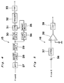
- the present invention relates to a diversity receiver of a type which is provided with two antennae positioned with a certain space in between or two antennae having different characteristics, and which selects one antenna by a switching operation for connecting the selected antenna with the receiver, and more particularly, to a diversity receiver which is suitable for use in an FM radio receiver equipped in a motor vehicle.
- a prior art diversity receiver is disclosed, for example, in Japanese Patent Laid-Open Publication No. 62-294340, in which one of the two antennae is selected in accordance with the noise level in the signal, and the selected antenna is connected to the receiver.
- the prior art diversity receiver includes first and second antennae 1 and 2 and antenna switching circuit 3 for selecting one of the first and second antennae 1 and 2.
- Front end 4, IF amplifier 5, and FM detector 6 are provided for converting the FM radio signal received at the antenna to an IF (intermediate frequency) signal, amplifying, and FM detecting the IF signal, respectively.
- Stereo multiplexer 7 is provided for separating right and left channel stereo signals from the output signal of FM detector 6.
- a combination of high-pass filter 8 and noise wave detector 9 define a noise detection circuit 10 which detects the high frequency noise signal in the output signal of FM detector 6.
- a trigger circuit 11 is provided for producing a trigger pulse when the output signal from noise detection circuit 10 is greater than a predetermined level, and T-FF (trigger flip-flop) 12 is provided for producing a switching signal according to the trigger pulse.
- a diversity receiver of this type switches the antenna when high frequency noise signal as detected by the FM detector 6 becomes greater than the predetermined level, and thereby maintaining good FM signal reception.
- a diversity receiver of the type shown in Fig. 1 further includes a counter 13 which counts the trigger pulses generated by trigger circuit 11, and a monostable multivibrator 14 which controls the operation of counter 13. By a control signal generated from counter 13 in accordance with the generation frequency of the trigger pulse, the stereo separation of the stereo multiplexer 7 is controlled to reduce the noise level.
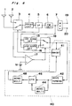
- a diversity receiver which has a first and second antennas for receiving an RF-signal and an antenna switching circuit for selecting one of the first and second antennas.
- the switching of the antenna is first carried out through the output of a first comparator only and then on the basis of the outputs of two comparators. Therefore, the intensity of the electric field of the detected signal is evaluated by two comparators, thereby providing hysteresis between the first switching and the second switching.
- the present invention has been developed with a view to substantially solving the above described disadvantages and has for its essential object to provide an improved diversity receiver which can provide an accurate noise detection both under strong and weak field strength.
- a diversity receiver comprises first and second noise detection circuits for detecting the noise signal included in the received signal, a field strength detection circuit for detecting the field strength of the received signal, and a selection circuit for selecting and outputting the output signal of the first or second noise detection circuit according to the output signal of the field strength detection circuit.
- the detection sensitivity of the first noise detection circuit is set high and the detection sensitivity of the second noise detection circuit is set low.
- the first output signal will be generated by the field strength detection circuit, whereby detection of the noise signal using the high sensitivity first noise detection circuit is possible, and the problem of insufficient sensitivity does not occur.
- the second output signal will be outputted from the field strength detection circuit, whereby the detection of the noise signal using the low sensitivity second noise detection circuit is possible, and improper operation does not occur.
- reference number 15 is a first noise detection circuit with a high sensitivity
- 16 is a second noise detection circuit with a low sensitivity
- 17 is a field strength detection circuit which compares a signal expressing the field strength of the received signal obtained from IF amplifier 5 with a predetermined reference voltage Vr and produces a first or second output signal when the signal expressing the field strength is higher or lower, respectively, than the predetermined reference voltage Vr.
- Reference number 18 is a selector for selecting the output signal of either first or second noise detection circuit 15 or 16 according to the output signal of the field strength detection circuit 17, and thus controls antenna switching circuit 3.
- antenna switching circuit 3 and selector 18 are connected in a manner as shown in Fig. 2, so that the required signal processing is performed by IF amplifier 5, FM detector 6, and stereo multiplexer 7, and thus, left-right stereo signals are obtained at the first and second output terminals 19 and 20.
- the high frequency noise signal contained in the output signal of FM detector 6 is applied to first and second noise detection circuits 15 and 16.
- Each of the first and second noise detection circuits 15 and 16 produces an output signal according to the high frequency noise signal, such as a multipass noise signal.
- the signal indicative of the field strength of the received signal as produced from IF amplifier 5 is applied to field strength detection circuit 17, which in turn produces either a first (e.g., low) level or a second (e.g., high) level output signal which is applied to selector 18.
- selector 18 provides no noise detection signal to antenna switching circuit 3, so that antenna switching circuit 3 is maintained in the state shown in Fig. 2, thereby continuing the normal reception using the first antenna 1.
- the level of high frequency noise signal contained in the output signal of FM detector 6 becomes high.
- This high noise level is detected by the first noise detection circuit 15 which then produces a corresponding noise detection signal.
- the noise detection signal is transmitted from first noise detection circuit 15 through selector 18 to antenna switching circuit 3.
- antenna switching circuit 3 switches the connection of the antenna from antenna 1 to antenna 2, so that the front end 4 starts to receive the RF signal from antenna 2.
- the first noise detection circuit 15 detects a high noise signal level in the signal produced from FM detector 6, so that first noise detection circuit 15 again produces a noise detection signal which is applied through selector 18 to antenna switching circuit 3.
- antenna switching circuit 3 switches the connection of the antenna from antenna 2 back to antenna 1.
- selector 18 switches to the position which is the opposite of that shown in Fig. 2, so that the output of the second noise detection circuit 16 is selected.
- the detection sensitivity of the second noise detection circuit 16 is set lower than that of the first noise detection circuit 15.
- second noise detection circuit 16 does not respond to white noise and other aberrations caused by a weak field strength, and is therefore able to detect accurately only noise signal which is not dependent upon field strength, e.g., multipass noise signal. Therefore, noise signal contained in the output of FM detector 6 is detected by second noise detection circuit 16, and when a noise detection signal is produced from second noise detection circuit 16, it is applied to antenna switching circuit 3 through selector 18 so that the antenna switching circuit 3 switches the antenna between the position shown in Fig. 2 and the position opposite that shown in Fig. 2. Thus, RF signal reception by the antenna is switched from that using the first antenna 1 to that using the second antenna 2, or vice versa. If noise signal is again detected in this state, antenna switching will once again occur.
- noise signals caused by multipasses can be accurately detected irrespective of the field strength of the received signal, and antenna switching can effectively occur.
- FIG. 3 a circuit diagram of a modification of the first and second noise detection circuits 15 and 16 is shown, in which a counter is used as the first and second noise detection circuits 15 and 16.
- the high frequency noise signal contained in the output of FM detector 6 is applied to a high pass filter 24 and in turn to a wave forming circuit 22.
- Wave forming circuit 22 produces a rectangular pulse corresponding to the noise signal exceeding a specified level.
- the rectangular pulse is then applied to the counter 23 for counting the number of rectangular pulses generated.
- counter 23 counts, for example, three rectangular pulses
- counter 23 produces a high level signal from its first output terminal 25
- counter 23 counts, for example, ten pulses
- counter 23 produces a high level signal from its second output terminal 26.
- the noise detection circuit shown in Fig. 3 operates as a first noise detection circuit of high sensitivity when selector 18 is in a state as shown in Fig. 3, and operates as a second noise detection circuit of low sensitivity when the selector 18 is in a state opposite that shown in Fig. 3.
- circuitry can be simplified because a single counter can be shared, and the sensitivity setting can be changed by simply changing the count value.
- FIG. 4 a circuit diagram of a modification of the first noise detection circuit 15 is shown, in which 27 is a bandpass filter for filtering and detecting the high frequency noise signal in the output signal from FM detector 6, 28 is a noise signal amplifier for amplifying the high frequency noise signal, 29 is a noise signal detector for detecting the output signal (representing the noise) from noise amplifier 28, 30 is a pulse generator for generating a pulse when the noise detected output signal from noise signal detector 29 exceeds a predetermined threshold level, 31 is a counter, 32 is a trigger circuit which generates a trigger signal according to the output signal of counter 31, 33 is a T-FF (trigger flip-flop) which is triggered by the output signal of the trigger circuit 32, and 34 and 35 are a level detector and monostable multivibrator, respectively, which control the operation of the counter 31 such that counter 31 counts only during the high level signal produced from the multivibrator 35.
- 27 is a bandpass filter for filtering and detecting the high frequency noise signal in the output signal from FM detector 6
- the circuit shown in Fig. 4 has a noise amplifier 28 between the bandpass filter 27 and noise signal detector 29 so that the high frequency noise signal passing the bandpass filter 27 can be amplified to a sufficient level and thus the noise detection of high sensitivity can be realized.
- a circuit diagram of a modification of the second noise detection circuit 16 which includes a capacitor 36 for cutting DC component and passing high frequency noise signal, an integrator 37, a comparator 38, and a T-FF 39.
- the AC component which is the noise signal, contained in the detected signal obtained from FM detector 6 is integrated with a long time constant and compared with a reference voltage.
- white noise caused by a weak field strength will not be detected due to the low sensitivity. Thus, the noise signals caused by a multipass can be accurately detected.
- Signal blocking circuit 40 includes a transmission inhibit circuit 41, a wave forming circuit 42 for waveforming the noise detection signal obtained from selector 18, a monostable multivibrator 44 for producing a pulse having a predetermined period of duration (such as 1 second) in response to the noise detection signal (a very narrow pulse signal), a counter 46 for counting the number of noise detection signals during a period in which monostable multivibrator 44 is producing a pulse and for producing a trigger pulse when counter has counted more than a predetermined number of noise detection signals, such as three noise detection signals, during the pulse duration, and a monostable multivibrator 48 for producing a pulse having a predetermined pulse duration in response to the trigger pulse from counter 46.
- transmission inhibit circuit 41 stops transmitting the output of selector 18 to antenna switching circuit 3.
- signal blocking circuit 40 blocks the transmission so as to prevent the high frequency noise detection signals from being transmitted to antenna switching circuit 3. Accordingly, when the noise signal is captured by both antennae 1 and 2, frequent antenna switching by antenna switching circuit 3 can be prevented, and sounds irritating to the listener can be prevented.
- a modification of the signal blocking circuit 40 which includes transmission inhibit circuit 41 and a field strength detector 43 which is defined by a comparator having its inverting input connected to the IF circuit 5 and non-inverting input connected to a predetermined reference voltage Ve which is smaller than the predetermined reference voltage Vr.
- the output of comparator 43 is connected to transmission inhibit circuit 41.
- comparator 43 produces a high level signal which is applied to transmission inhibit circuit 41.
- the signal transmission from selector 18 to antenna switching circuit 3 is blocked to prevent the antenna switching operation between antennae 1 and 2.
- antenna switching when the field strength of the received signal is extremely low will not occur, and unnecessary antenna switching can be prevented before such may occur.
- a diversity receiver uses two noise detection circuits with varying high and low sensitivity levels according to the field strength of the received signal, and therefore, correct antenna switching will be carried out.
Landscapes
- Engineering & Computer Science (AREA)
- Computer Networks & Wireless Communication (AREA)
- Signal Processing (AREA)
- Radio Transmission System (AREA)
Description
- The present invention relates to a diversity receiver of a type which is provided with two antennae positioned with a certain space in between or two antennae having different characteristics, and which selects one antenna by a switching operation for connecting the selected antenna with the receiver, and more particularly, to a diversity receiver which is suitable for use in an FM radio receiver equipped in a motor vehicle.
- A prior art diversity receiver is disclosed, for example, in Japanese Patent Laid-Open Publication No. 62-294340, in which one of the two antennae is selected in accordance with the noise level in the signal, and the selected antenna is connected to the receiver. As shown in Fig. 1, the prior art diversity receiver includes first and
second antennae antenna switching circuit 3 for selecting one of the first andsecond antennae Front end 4,IF amplifier 5, andFM detector 6 are provided for converting the FM radio signal received at the antenna to an IF (intermediate frequency) signal, amplifying, and FM detecting the IF signal, respectively.Stereo multiplexer 7 is provided for separating right and left channel stereo signals from the output signal ofFM detector 6. A combination of high-pass filter 8 andnoise wave detector 9 define anoise detection circuit 10 which detects the high frequency noise signal in the output signal ofFM detector 6. Atrigger circuit 11 is provided for producing a trigger pulse when the output signal fromnoise detection circuit 10 is greater than a predetermined level, and T-FF (trigger flip-flop) 12 is provided for producing a switching signal according to the trigger pulse. - A diversity receiver of this type switches the antenna when high frequency noise signal as detected by the
FM detector 6 becomes greater than the predetermined level, and thereby maintaining good FM signal reception. In addition, a diversity receiver of the type shown in Fig. 1 further includes acounter 13 which counts the trigger pulses generated bytrigger circuit 11, and amonostable multivibrator 14 which controls the operation ofcounter 13. By a control signal generated fromcounter 13 in accordance with the generation frequency of the trigger pulse, the stereo separation of thestereo multiplexer 7 is controlled to reduce the noise level. - Therefore, if the circuit as shown in Fig. 1 is used, good reception with no noise signal can be obtained.
- However, in a diversity receiver as shown in Fig. 1, if the detection sensitivity of the noise signal is increased, erroneous operation caused by white noise during reception of weak field signals may easily occur. Furthermore, if detection sensitivity of the noise signal is lowered to prevent such an erroneous operation, the sensitiviy will be insufficient for signals of a middle or strong field strength, and accurate detection of the noise signal will not be possible.
- From US-A-4 633 519 a diversity receiver is known which has a first and second antennas for receiving an RF-signal and an antenna switching circuit for selecting one of the first and second antennas. In this apparatus the switching of the antenna is first carried out through the output of a first comparator only and then on the basis of the outputs of two comparators. Therefore, the intensity of the electric field of the detected signal is evaluated by two comparators, thereby providing hysteresis between the first switching and the second switching.
- The present invention has been developed with a view to substantially solving the above described disadvantages and has for its essential object to provide an improved diversity receiver which can provide an accurate noise detection both under strong and weak field strength.
- In accomplishing these and other objects, a diversity receiver according to the present invention comprises first and second noise detection circuits for detecting the noise signal included in the received signal, a field strength detection circuit for detecting the field strength of the received signal, and a selection circuit for selecting and outputting the output signal of the first or second noise detection circuit according to the output signal of the field strength detection circuit.
- In a diversity receiver according to the present invention, the detection sensitivity of the first noise detection circuit is set high and the detection sensitivity of the second noise detection circuit is set low. Thus, when the field strength of the received signal is strong, the first output signal will be generated by the field strength detection circuit, whereby detection of the noise signal using the high sensitivity first noise detection circuit is possible, and the problem of insufficient sensitivity does not occur. Furthermore, when the field strength of the received signal is weak, the second output signal will be outputted from the field strength detection circuit, whereby the detection of the noise signal using the low sensitivity second noise detection circuit is possible, and improper operation does not occur.
- These and other objects and features of the present invention will become apparent from the following description taken in conjunction with preferred embodiments thereof with reference to the accompanying drawings, throughout which like parts are designated by like reference numerals, and in which:
- Fig. 1 is a circuit diagram showing a conventional diversity receiver;
- Fig. 2 is a circuit diagram of a diversity receiver according to a preferred embodiment of the present invention;
- Fig. 3 is a circuit diagram showing an alternative embodiment of the first and second noise detection circuits shown in Fig. 2;
- Fig. 4 is a circuit diagram showing a modification of the first noise detection circuit shown in Fig. 2;
- Fig. 5 is a circuit diagram showing a modification of the second noise detection circuit shown in Fig. 2;
- Fig. 6 is a circuit diagram showing a modification which further has a signal blocking circuit; and
- Fig. 7 is a circuit diagram similar to Fig. 6, but showing a modification thereof.
- Referring to Fig. 2, a circuit diagram of a first embodiment according to the present invention is shown in which
reference number 15 is a first noise detection circuit with a high sensitivity, 16 is a second noise detection circuit with a low sensitivity, 17 is a field strength detection circuit which compares a signal expressing the field strength of the received signal obtained fromIF amplifier 5 with a predetermined reference voltage Vr and produces a first or second output signal when the signal expressing the field strength is higher or lower, respectively, than the predetermined reference voltage Vr.Reference number 18 is a selector for selecting the output signal of either first or secondnoise detection circuit strength detection circuit 17, and thus controlsantenna switching circuit 3. - In operation, if
antenna switching circuit 3 andselector 18 are connected in a manner as shown in Fig. 2, the RF signal received atfirst antenna 1 is transmitted to thefront end 4, so that the required signal processing is performed byIF amplifier 5,FM detector 6, andstereo multiplexer 7, and thus, left-right stereo signals are obtained at the first andsecond output terminals - Furthermore, the high frequency noise signal contained in the output signal of
FM detector 6 is applied to first and secondnoise detection circuits noise detection circuits IF amplifier 5 is applied to fieldstrength detection circuit 17, which in turn produces either a first (e.g., low) level or a second (e.g., high) level output signal which is applied toselector 18. - When the field strength of the RF signal received at the
first antenna 1 is sufficiently high, the level of the signal transmitted fromIF amplifier 5 to fieldstrength detection circuit 17 is greater than the predetermined reference voltage Vr, and thus, a low level first output signal is produced from fieldstrength detection circuit 17. In this state,selector 18 maintains the position as shown in Fig. 2, and thus the output signal of firstnoise detection circuit 15 is transmitted throughselector 18 toantenna switching circuit 3. - If a multipass condition or any other noise generation condition does not arise, no noise detection signal is produced from
first detection circuit 15. Thus,selector 18 provides no noise detection signal toantenna switching circuit 3, so thatantenna switching circuit 3 is maintained in the state shown in Fig. 2, thereby continuing the normal reception using thefirst antenna 1. - If, for example, a multipass condition occurs in the RF signal received by
antenna 1, the level of high frequency noise signal contained in the output signal ofFM detector 6 becomes high. This high noise level is detected by the firstnoise detection circuit 15 which then produces a corresponding noise detection signal. The noise detection signal is transmitted from firstnoise detection circuit 15 throughselector 18 toantenna switching circuit 3. Thus, antenna switchingcircuit 3 switches the connection of the antenna fromantenna 1 toantenna 2, so that thefront end 4 starts to receive the RF signal fromantenna 2. - Thereafter, if a multipass condition occurs in the RF signal received by
antenna 2, the firstnoise detection circuit 15 detects a high noise signal level in the signal produced fromFM detector 6, so that firstnoise detection circuit 15 again produces a noise detection signal which is applied throughselector 18 toantenna switching circuit 3. Thus, antenna switchingcircuit 3 switches the connection of the antenna fromantenna 2 back toantenna 1. - Then, if the field strength of the received signal drops, the level of the signal transmitted from
IF amplifier 5 to fieldstrength detection circuit 17 becomes lower than the reference voltage Vr, and thus a high level second signal is produced from fieldstrength detection circuit 17. Thus,selector 18 switches to the position which is the opposite of that shown in Fig. 2, so that the output of the secondnoise detection circuit 16 is selected. - As previously described, the detection sensitivity of the second
noise detection circuit 16 is set lower than that of the firstnoise detection circuit 15. Thus, secondnoise detection circuit 16 does not respond to white noise and other aberrations caused by a weak field strength, and is therefore able to detect accurately only noise signal which is not dependent upon field strength, e.g., multipass noise signal. Therefore, noise signal contained in the output ofFM detector 6 is detected by secondnoise detection circuit 16, and when a noise detection signal is produced from secondnoise detection circuit 16, it is applied toantenna switching circuit 3 throughselector 18 so that theantenna switching circuit 3 switches the antenna between the position shown in Fig. 2 and the position opposite that shown in Fig. 2. Thus, RF signal reception by the antenna is switched from that using thefirst antenna 1 to that using thesecond antenna 2, or vice versa. If noise signal is again detected in this state, antenna switching will once again occur. - Therefore, if a diversity receiver such as shown in Fig. 2 is used, noise signals caused by multipasses can be accurately detected irrespective of the field strength of the received signal, and antenna switching can effectively occur.
- Referring to Fig. 3, a circuit diagram of a modification of the first and second
noise detection circuits noise detection circuits FM detector 6 is applied to ahigh pass filter 24 and in turn to awave forming circuit 22.Wave forming circuit 22 produces a rectangular pulse corresponding to the noise signal exceeding a specified level. The rectangular pulse is then applied to thecounter 23 for counting the number of rectangular pulses generated. Whencounter 23 counts, for example, three rectangular pulses,counter 23 produces a high level signal from itsfirst output terminal 25, and whencounter 23 counts, for example, ten pulses,counter 23 produces a high level signal from itssecond output terminal 26. Therefore, the noise detection circuit shown in Fig. 3 operates as a first noise detection circuit of high sensitivity whenselector 18 is in a state as shown in Fig. 3, and operates as a second noise detection circuit of low sensitivity when theselector 18 is in a state opposite that shown in Fig. 3. - It is to be noted that if the circuit as shown in Fig. 3 is used, the circuitry can be simplified because a single counter can be shared, and the sensitivity setting can be changed by simply changing the count value.
- Referring to Fig. 4, a circuit diagram of a modification of the first
noise detection circuit 15 is shown, in which 27 is a bandpass filter for filtering and detecting the high frequency noise signal in the output signal fromFM detector noise amplifier noise signal detector 29 exceeds a predetermined threshold level, 31 is a counter, 32 is a trigger circuit which generates a trigger signal according to the output signal ofcounter trigger circuit counter 31 such that counter 31 counts only during the high level signal produced from themultivibrator 35. - The circuit shown in Fig. 4 has a
noise amplifier 28 between thebandpass filter 27 andnoise signal detector 29 so that the high frequency noise signal passing thebandpass filter 27 can be amplified to a sufficient level and thus the noise detection of high sensitivity can be realized. - Referring to Fig. 5, a circuit diagram of a modification of the second
noise detection circuit 16 is shown which includes acapacitor 36 for cutting DC component and passing high frequency noise signal, anintegrator 37, acomparator 38, and a T-FF 39. When the circuit shown in Fig. 5 is employed, the AC component, which is the noise signal, contained in the detected signal obtained fromFM detector 6 is integrated with a long time constant and compared with a reference voltage. When the circuit of Fig. 5 is employed, white noise caused by a weak field strength will not be detected due to the low sensitivity. Thus, the noise signals caused by a multipass can be accurately detected. - Referring to Fig. 6, another modification is shown in which a
signal blocking circuit 40 is inserted betweenselector 18 andantenna switching circuit 3. Signal blockingcircuit 40 includes a transmission inhibitcircuit 41, awave forming circuit 42 for waveforming the noise detection signal obtained fromselector 18, amonostable multivibrator 44 for producing a pulse having a predetermined period of duration (such as 1 second) in response to the noise detection signal (a very narrow pulse signal), acounter 46 for counting the number of noise detection signals during a period in whichmonostable multivibrator 44 is producing a pulse and for producing a trigger pulse when counter has counted more than a predetermined number of noise detection signals, such as three noise detection signals, during the pulse duration, and amonostable multivibrator 48 for producing a pulse having a predetermined pulse duration in response to the trigger pulse fromcounter 46. During when themonostable multivibrator 48 is producing a pulse, transmission inhibitcircuit 41 stops transmitting the output ofselector 18 toantenna switching circuit 3. - By the circuit Fig. 6, when either one of the first and
second noise detectors circuit 40 blocks the transmission so as to prevent the high frequency noise detection signals from being transmitted toantenna switching circuit 3. Accordingly, when the noise signal is captured by bothantennae antenna switching circuit 3 can be prevented, and sounds irritating to the listener can be prevented. - Referring to Fig. 7, a modification of the
signal blocking circuit 40 is shown, which includes transmission inhibitcircuit 41 and afield strength detector 43 which is defined by a comparator having its inverting input connected to theIF circuit 5 and non-inverting input connected to a predetermined reference voltage Ve which is smaller than the predetermined reference voltage Vr. The output ofcomparator 43 is connected to transmission inhibitcircuit 41. - By the circuit of Fig. 7, when the field strength becomes very weak, which is weaker than that detected by the
field strength detector 17,comparator 43 produces a high level signal which is applied to transmission inhibitcircuit 41. Thus, when the field strength is very weak, the RF signal reception condition will hardly change even when theantennae selector 18 toantenna switching circuit 3 is blocked to prevent the antenna switching operation betweenantennae - As will be understood from the above description, a diversity receiver according to the present invention uses two noise detection circuits with varying high and low sensitivity levels according to the field strength of the received signal, and therefore, correct antenna switching will be carried out.
- Although the present invention has been fully described in connection with the preferred embodiments thereof with reference to the accompanying drawings, it is to be noted that various changes and modifications are apparent to those skilled in the art. Such changes and modifications are to be understood as included within the scope of the present invention as defined by the appended claims unless they depart therefrom.
Claims (9)
- A diversity receiver comprising:
first (1) and second (2) antennas for receiving an RF signal; and
an antenna switching circuit (3) for selecting one of said first (1) and second (2) antennas;
characterized by
a first detection circuit (15), having a high sensitivity, for detecting a noise signal contained within the received RF signal;
a second detection circuit (16), having a low sensitivity, for detecting a noise signal contained within the received RF signal;
a field strength detection circuit (17) for detecting a field strength of the received RF signal; and
a selection circuit (18) for selecting either one of the first and second detection circuits (15, 16) according to the output signal of said field strength detection circuit (17), and for providing a switching signal to said antenna switching circuit (3) for switching the selection of said antenna;
whereby when the field strength is relatively strong, said first detection circuit (15) with high sensitivity is used for the noise detection, and when the field strength is relatively weak, said second detection circuit (16) with low sensitivity is used for the noise detection. - A diversity receiver according to Claim 1, wherein said selection circuit selects an output of said first detection circuit (15) when the field strength of the received signal is greater than a predetermined level (Vr).
- A diversity receiver according to Claim 1, wherein said first detection circuit comprises (15) a first counter (29) for counting pulses corresponding to said noise signals and for producing a first output signal (25) when the value of said first counter exceeds a first predetermined value, and wherein said second detection circuit comprises a second counter for counting pulses corresponding to said noise signals and for producing a second output signal (26) when the value of said second counter exceeds a second predetermined value which is greater than said first predetermined value.
- A diversity receiver according to Claim 3 wherein said first and second counters (15, 16) are comprised of a common counter (23) in such a manner that a first output signal (25) is output when the value of the common counter reaches a first predetermined value, and a second output signal (26) is output when the value of the common counter reaches a second predetermined value which is greater than said first predetermined value.
- A diversity receiver according to Claim 1 wherein said first detection circuit comprises a third counter (31) for counting a number of noise pulses and for producing a noise signal upon counting a predetermined number of noise pulses.
- A diversity receiver according to Claim 1 wherein said second detection circuit comprises an integrator (37) for integrating a noise signal, and a comparator (38) for comparing the integrated signal with a predetermined level.
- A diversity receiver according to Claim 1 further comprising a signal blocking circuit (40) inserted between said selection circuit (18) and said antenna switching circuit (3) for blocking the transmission of said switching signal to said antenna switching circuit.
- A diversity receiver according to Claim 7, wherein said signal blocking circuit (40) comprises an inhibit circuit (41) inserted between said selection circuit (18) and said antenna switching circuit (3), a fourth counter (46) for counting the number of noise signals produced in a predetermined period of time, and a pulse generator (48) for generating, when the value of said fourth counter exceeds a second predetermined value, an inhibit pulse having a predetermined pulse width to said inhibit circuit (41), whereby said inhibit circuit stops the transmission of said switching signal to said antenna switching circuit during the presence of said inhibit pulse.
- A diversity receiver according to Claim 7, wherein said signal blocking circuit comprises an inhibit circuit (41) inserted between said selection circuit (18) and said antenna switching circuit (3) and a second field strength detection circuit (43) for detecting a field strength of the received RF signal and for producing an inhibit signal during when the field strength is lower than a predetermined field strength, whereby said inhibit circuit (41) stops the transmission of said switching signal to said antenna switching circuit (3) during the presence of said inhibit signal.
Applications Claiming Priority (2)
| Application Number | Priority Date | Filing Date | Title |
|---|---|---|---|
| JP63122317A JP2708777B2 (en) | 1988-05-19 | 1988-05-19 | Diversity receiver |
| JP122317/88 | 1988-05-19 |
Publications (3)
| Publication Number | Publication Date |
|---|---|
| EP0343538A2 EP0343538A2 (en) | 1989-11-29 |
| EP0343538A3 EP0343538A3 (en) | 1991-05-02 |
| EP0343538B1 true EP0343538B1 (en) | 1995-10-18 |
Family
ID=14832964
Family Applications (1)
| Application Number | Title | Priority Date | Filing Date |
|---|---|---|---|
| EP89109094A Expired - Lifetime EP0343538B1 (en) | 1988-05-19 | 1989-05-19 | Diversity receiver |
Country Status (5)
| Country | Link |
|---|---|
| US (1) | US4977615A (en) |
| EP (1) | EP0343538B1 (en) |
| JP (1) | JP2708777B2 (en) |
| KR (1) | KR960000526B1 (en) |
| DE (1) | DE68924554T2 (en) |
Families Citing this family (37)
| Publication number | Priority date | Publication date | Assignee | Title |
|---|---|---|---|---|
| CA1320535C (en) * | 1988-02-29 | 1993-07-20 | Kazuzi Watanabe | Interference cancellation circuit |
| US5157672A (en) * | 1989-03-15 | 1992-10-20 | Nec Corporation | Interference detection apparatus for use in digital mobile communications system |
| US5390342A (en) * | 1990-03-14 | 1995-02-14 | Pioneer Electronic Corporation | Receiver using selective diversity receiving system |
| GB9019487D0 (en) * | 1990-09-06 | 1990-10-24 | Ncr Co | Carrier detection for a wireless local area network |
| GB9019489D0 (en) * | 1990-09-06 | 1990-10-24 | Ncr Co | Antenna control for a wireless local area network station |
| US5369801A (en) * | 1992-09-25 | 1994-11-29 | Northern Telecom Limited | Antenna diversity reception in wireless personal communications |
| CA2125220C (en) * | 1993-06-08 | 2000-08-15 | Joji Kane | Noise suppressing apparatus capable of preventing deterioration in high frequency signal characteristic after noise suppression and in balanced signal transmitting system |
| ATE240618T1 (en) * | 1993-09-30 | 2003-05-15 | Conexant Systems Inc | BASE STATION FOR A DIGITAL CORDLESS TELEPHONE WITH MULTIPLE ANTENNA ARRANGEMENT |
| DE4403612B4 (en) * | 1994-02-05 | 2008-10-02 | Lindenmeier, Heinz, Prof. Dr. Ing. | Circuit arrangement for a multi-antenna scanning diversity system for motor vehicles |
| WO1996012355A2 (en) * | 1994-10-17 | 1996-04-25 | Philips Electronics N.V. | A wireless digital communication system, a radio apparatus, a digital speaker, and a digital speaker controlling apparatus |
| US5603107A (en) * | 1995-06-09 | 1997-02-11 | Ford Motor Company | Switching system for diversity antenna FM receiver |
| US5818543A (en) * | 1995-09-06 | 1998-10-06 | Premier Wireless, Inc. | Diversity receiver for television |
| JP3297580B2 (en) * | 1996-02-26 | 2002-07-02 | キヤノン株式会社 | Spread spectrum communication equipment |
| CA2188845A1 (en) * | 1996-10-25 | 1998-04-25 | Stephen Ross Todd | Diversity Antenna Selection |
| US6108526A (en) * | 1997-05-07 | 2000-08-22 | Lucent Technologies, Inc. | Antenna system and method thereof |
| US5933111A (en) * | 1997-06-17 | 1999-08-03 | A T & T Corp. | Apparatus and method for detection of antenna mispointing in satellite earth stations |
| SE9702370L (en) * | 1997-06-19 | 1998-12-20 | Ericsson Telefon Ab L M | Balanced diversity |
| KR100298345B1 (en) * | 1997-12-31 | 2001-08-07 | 윤종용 | System of selection diversity for ct-2 system |
| EP1020828B1 (en) * | 1998-07-30 | 2005-09-21 | Mitsubishi Denki Kabushiki Kaisha | Emergency reporting apparatus with self-diagnostic function |
| JP2001184149A (en) * | 1999-12-27 | 2001-07-06 | Toshiba Corp | Information processing apparatus and operation state control method |
| EP1150440B1 (en) * | 2000-04-28 | 2006-07-12 | Siemens Aktiengesellschaft | Antenna diversity receiver |
| JP4417593B2 (en) * | 2001-08-10 | 2010-02-17 | パイオニア株式会社 | Antenna switching device |
| JP4460226B2 (en) * | 2002-02-21 | 2010-05-12 | パナソニック株式会社 | Radio base station apparatus, radio terminal apparatus, and radio communication method |
| JP3880485B2 (en) * | 2002-08-22 | 2007-02-14 | 株式会社豊田自動織機 | Stereo demodulation circuit |
| JP2004128930A (en) * | 2002-10-03 | 2004-04-22 | Toyota Industries Corp | FM receiver, noise removing apparatus for FM receiver, and noise removing method |
| DE10311836B4 (en) * | 2003-03-18 | 2006-10-05 | Integrated Electronic Systems !Sys Consulting Gmbh | Remote controlled industrial device |
| KR20050013333A (en) * | 2003-07-28 | 2005-02-04 | 현대자동차주식회사 | Radio receiver for a vehicle and method thereof |
| JP2005252933A (en) * | 2004-03-08 | 2005-09-15 | Matsushita Electric Ind Co Ltd | AM radio receiver |
| TWI289385B (en) * | 2005-01-07 | 2007-11-01 | Neuro Solution Corp | FM radio receiver |
| JP2006287845A (en) * | 2005-04-05 | 2006-10-19 | Fujitsu Ten Ltd | Diversity receiver and signal processing circuit |
| JP2009081839A (en) * | 2007-09-04 | 2009-04-16 | Sanyo Electric Co Ltd | FM tuner |
| JP4941338B2 (en) * | 2008-02-01 | 2012-05-30 | 富士通株式会社 | Communication apparatus, noise removal method, and computer program |
| JP2009278525A (en) * | 2008-05-16 | 2009-11-26 | Nec Electronics Corp | Antenna diversity receiver and antenna switching control method therefor |
| EP2207273B1 (en) * | 2009-01-09 | 2016-01-06 | AKG Acoustics GmbH | Method and device for receiving digital audio data |
| AR086723A1 (en) * | 2011-06-22 | 2014-01-15 | Vam Drilling France | TUBULAR RADIO FREQUENCY COMMUNICATION DEVICE FOR DRILLING WELL HEAD |
| US8600331B2 (en) * | 2012-04-11 | 2013-12-03 | Black Berry Limited | Radio receiver with reconfigurable baseband channel filter |
| JP7078018B2 (en) * | 2019-06-26 | 2022-05-31 | 株式会社Jvcケンウッド | Receiver and receive processing program |
Family Cites Families (7)
| Publication number | Priority date | Publication date | Assignee | Title |
|---|---|---|---|---|
| JPS57135532A (en) * | 1981-02-13 | 1982-08-21 | Matsushita Electric Ind Co Ltd | Diversity receiver |
| JPS57135533A (en) * | 1981-02-13 | 1982-08-21 | Matsushita Electric Ind Co Ltd | Diversity receiver |
| JPS58191538A (en) * | 1982-04-30 | 1983-11-08 | Clarion Co Ltd | Diversity receiver for car mounting |
| US4499606A (en) * | 1982-12-27 | 1985-02-12 | Sri International | Reception enhancement in mobile FM broadcast receivers and the like |
| JPS59181732A (en) * | 1983-03-31 | 1984-10-16 | Toshiba Corp | Diversity receiving system in portable radio equipment |
| JPH0314850Y2 (en) * | 1984-10-15 | 1991-04-02 | ||
| JPH0771034B2 (en) * | 1986-05-19 | 1995-07-31 | 三洋電機株式会社 | Diversity receiver |
-
1988
- 1988-05-19 JP JP63122317A patent/JP2708777B2/en not_active Expired - Lifetime
-
1989
- 1989-05-16 US US07/352,775 patent/US4977615A/en not_active Expired - Lifetime
- 1989-05-18 KR KR1019890006604A patent/KR960000526B1/en not_active Expired - Fee Related
- 1989-05-19 EP EP89109094A patent/EP0343538B1/en not_active Expired - Lifetime
- 1989-05-19 DE DE68924554T patent/DE68924554T2/en not_active Expired - Lifetime
Also Published As
| Publication number | Publication date |
|---|---|
| DE68924554D1 (en) | 1995-11-23 |
| KR890017902A (en) | 1989-12-18 |
| EP0343538A2 (en) | 1989-11-29 |
| US4977615A (en) | 1990-12-11 |
| JP2708777B2 (en) | 1998-02-04 |
| EP0343538A3 (en) | 1991-05-02 |
| KR960000526B1 (en) | 1996-01-08 |
| JPH01292915A (en) | 1989-11-27 |
| DE68924554T2 (en) | 1996-06-05 |
Similar Documents
| Publication | Publication Date | Title |
|---|---|---|
| EP0343538B1 (en) | Diversity receiver | |
| US4499606A (en) | Reception enhancement in mobile FM broadcast receivers and the like | |
| EP0792017B1 (en) | High-frequency radio signal receiving apparatus for digital communication | |
| US4370522A (en) | FM Receiver for use with motorcars | |
| EP0286366B1 (en) | Space diversity receiving system | |
| EP0208530B1 (en) | Squelch detecting circuit with squelch start determining means | |
| EP0217475A1 (en) | Receiver including a multipath transmission detector | |
| JPS6139731A (en) | Noise detector | |
| US5444862A (en) | Circuit for stopping data transmission responding to low level and rapid fall of received electric field | |
| EP0565255B1 (en) | Multipath detector using phase comparison of stereo pilot signal | |
| US4189679A (en) | Noise detecting circuit having noise-immune AGC | |
| US20050036568A1 (en) | Fast settling data slicer comprising a low-pass filter with switchable cut-off frequency and a notch-filter | |
| US4742570A (en) | Multipath noise detecting circuit | |
| EP0293873B1 (en) | A signal distinction circuit | |
| US4099124A (en) | Combined keyed AGC and pulse amplitude comparator circuit | |
| JP2620633B2 (en) | Diversity receiver | |
| JPH0730472A (en) | Diversity antenna switching control circuit | |
| EP1100208B1 (en) | Receiver with multipath interference dependent mono-stereo detector | |
| JPS60248082A (en) | Circuit for detecting presence or absence of video signal reception | |
| EP0477463A1 (en) | Multipath detector for an FM tuner | |
| JPS62189820A (en) | Noise discrimination circuit | |
| US6052570A (en) | RSSI comparison circuit for a time duplex system | |
| JPH0733471Y2 (en) | Diversity receiver | |
| GB2217150A (en) | Voice/speech operated switch | |
| JPH01233926A (en) | Automotive space diversity receiver switching device |
Legal Events
| Date | Code | Title | Description |
|---|---|---|---|
| PUAI | Public reference made under article 153(3) epc to a published international application that has entered the european phase |
Free format text: ORIGINAL CODE: 0009012 |
|
| AK | Designated contracting states |
Kind code of ref document: A2 Designated state(s): DE FR GB IT |
|
| 17P | Request for examination filed |
Effective date: 19901210 |
|
| PUAL | Search report despatched |
Free format text: ORIGINAL CODE: 0009013 |
|
| AK | Designated contracting states |
Kind code of ref document: A3 Designated state(s): DE FR GB IT |
|
| 17Q | First examination report despatched |
Effective date: 19930326 |
|
| GRAA | (expected) grant |
Free format text: ORIGINAL CODE: 0009210 |
|
| AK | Designated contracting states |
Kind code of ref document: B1 Designated state(s): DE FR GB IT |
|
| ITF | It: translation for a ep patent filed | ||
| REF | Corresponds to: |
Ref document number: 68924554 Country of ref document: DE Date of ref document: 19951123 |
|
| ET | Fr: translation filed | ||
| PLBE | No opposition filed within time limit |
Free format text: ORIGINAL CODE: 0009261 |
|
| STAA | Information on the status of an ep patent application or granted ep patent |
Free format text: STATUS: NO OPPOSITION FILED WITHIN TIME LIMIT |
|
| 26N | No opposition filed | ||
| REG | Reference to a national code |
Ref country code: GB Ref legal event code: IF02 |
|
| PGFP | Annual fee paid to national office [announced via postgrant information from national office to epo] |
Ref country code: DE Payment date: 20080522 Year of fee payment: 20 |
|
| PGFP | Annual fee paid to national office [announced via postgrant information from national office to epo] |
Ref country code: IT Payment date: 20080527 Year of fee payment: 20 |
|
| PGFP | Annual fee paid to national office [announced via postgrant information from national office to epo] |
Ref country code: GB Payment date: 20080521 Year of fee payment: 20 |
|
| REG | Reference to a national code |
Ref country code: GB Ref legal event code: PE20 Expiry date: 20090518 |
|
| PG25 | Lapsed in a contracting state [announced via postgrant information from national office to epo] |
Ref country code: GB Free format text: LAPSE BECAUSE OF EXPIRATION OF PROTECTION Effective date: 20090518 |
|
| PGFP | Annual fee paid to national office [announced via postgrant information from national office to epo] |
Ref country code: FR Payment date: 20080514 Year of fee payment: 20 |