EP0343375A1 - Method for cancelling of conductive-path interruptions - Google Patents
Method for cancelling of conductive-path interruptions Download PDFInfo
- Publication number
- EP0343375A1 EP0343375A1 EP89107071A EP89107071A EP0343375A1 EP 0343375 A1 EP0343375 A1 EP 0343375A1 EP 89107071 A EP89107071 A EP 89107071A EP 89107071 A EP89107071 A EP 89107071A EP 0343375 A1 EP0343375 A1 EP 0343375A1
- Authority
- EP
- European Patent Office
- Prior art keywords
- molded part
- conductor track
- conductor
- insulating film
- working window
- Prior art date
- Legal status (The legal status is an assumption and is not a legal conclusion. Google has not performed a legal analysis and makes no representation as to the accuracy of the status listed.)
- Granted
Links
Images
Classifications
-
- H—ELECTRICITY
- H05—ELECTRIC TECHNIQUES NOT OTHERWISE PROVIDED FOR
- H05K—PRINTED CIRCUITS; CASINGS OR CONSTRUCTIONAL DETAILS OF ELECTRIC APPARATUS; MANUFACTURE OF ASSEMBLAGES OF ELECTRICAL COMPONENTS
- H05K3/00—Apparatus or processes for manufacturing printed circuits
- H05K3/22—Secondary treatment of printed circuits
- H05K3/225—Correcting or repairing of printed circuits
-
- B—PERFORMING OPERATIONS; TRANSPORTING
- B23—MACHINE TOOLS; METAL-WORKING NOT OTHERWISE PROVIDED FOR
- B23K—SOLDERING OR UNSOLDERING; WELDING; CLADDING OR PLATING BY SOLDERING OR WELDING; CUTTING BY APPLYING HEAT LOCALLY, e.g. FLAME CUTTING; WORKING BY LASER BEAM
- B23K11/00—Resistance welding; Severing by resistance heating
- B23K11/002—Resistance welding; Severing by resistance heating specially adapted for particular articles or work
-
- B—PERFORMING OPERATIONS; TRANSPORTING
- B23—MACHINE TOOLS; METAL-WORKING NOT OTHERWISE PROVIDED FOR
- B23K—SOLDERING OR UNSOLDERING; WELDING; CLADDING OR PLATING BY SOLDERING OR WELDING; CUTTING BY APPLYING HEAT LOCALLY, e.g. FLAME CUTTING; WORKING BY LASER BEAM
- B23K11/00—Resistance welding; Severing by resistance heating
- B23K11/22—Severing by resistance heating
-
- B—PERFORMING OPERATIONS; TRANSPORTING
- B23—MACHINE TOOLS; METAL-WORKING NOT OTHERWISE PROVIDED FOR
- B23K—SOLDERING OR UNSOLDERING; WELDING; CLADDING OR PLATING BY SOLDERING OR WELDING; CUTTING BY APPLYING HEAT LOCALLY, e.g. FLAME CUTTING; WORKING BY LASER BEAM
- B23K2101/00—Articles made by soldering, welding or cutting
- B23K2101/36—Electric or electronic devices
- B23K2101/42—Printed circuits
-
- H—ELECTRICITY
- H05—ELECTRIC TECHNIQUES NOT OTHERWISE PROVIDED FOR
- H05K—PRINTED CIRCUITS; CASINGS OR CONSTRUCTIONAL DETAILS OF ELECTRIC APPARATUS; MANUFACTURE OF ASSEMBLAGES OF ELECTRICAL COMPONENTS
- H05K2201/00—Indexing scheme relating to printed circuits covered by H05K1/00
- H05K2201/10—Details of components or other objects attached to or integrated in a printed circuit board
- H05K2201/10227—Other objects, e.g. metallic pieces
- H05K2201/1028—Thin metal strips as connectors or conductors
-
- H—ELECTRICITY
- H05—ELECTRIC TECHNIQUES NOT OTHERWISE PROVIDED FOR
- H05K—PRINTED CIRCUITS; CASINGS OR CONSTRUCTIONAL DETAILS OF ELECTRIC APPARATUS; MANUFACTURE OF ASSEMBLAGES OF ELECTRICAL COMPONENTS
- H05K2203/00—Indexing scheme relating to apparatus or processes for manufacturing printed circuits covered by H05K3/00
- H05K2203/11—Treatments characterised by their effect, e.g. heating, cooling, roughening
- H05K2203/1115—Resistance heating, e.g. by current through the PCB conductors or through a metallic mask
-
- H—ELECTRICITY
- H05—ELECTRIC TECHNIQUES NOT OTHERWISE PROVIDED FOR
- H05K—PRINTED CIRCUITS; CASINGS OR CONSTRUCTIONAL DETAILS OF ELECTRIC APPARATUS; MANUFACTURE OF ASSEMBLAGES OF ELECTRICAL COMPONENTS
- H05K2203/00—Indexing scheme relating to apparatus or processes for manufacturing printed circuits covered by H05K3/00
- H05K2203/17—Post-manufacturing processes
- H05K2203/173—Adding connections between adjacent pads or conductors, e.g. for modifying or repairing
-
- H—ELECTRICITY
- H05—ELECTRIC TECHNIQUES NOT OTHERWISE PROVIDED FOR
- H05K—PRINTED CIRCUITS; CASINGS OR CONSTRUCTIONAL DETAILS OF ELECTRIC APPARATUS; MANUFACTURE OF ASSEMBLAGES OF ELECTRICAL COMPONENTS
- H05K3/00—Apparatus or processes for manufacturing printed circuits
- H05K3/30—Assembling printed circuits with electric components, e.g. with resistor
- H05K3/32—Assembling printed circuits with electric components, e.g. with resistor electrically connecting electric components or wires to printed circuits
- H05K3/328—Assembling printed circuits with electric components, e.g. with resistor electrically connecting electric components or wires to printed circuits by welding
-
- Y—GENERAL TAGGING OF NEW TECHNOLOGICAL DEVELOPMENTS; GENERAL TAGGING OF CROSS-SECTIONAL TECHNOLOGIES SPANNING OVER SEVERAL SECTIONS OF THE IPC; TECHNICAL SUBJECTS COVERED BY FORMER USPC CROSS-REFERENCE ART COLLECTIONS [XRACs] AND DIGESTS
- Y10—TECHNICAL SUBJECTS COVERED BY FORMER USPC
- Y10T—TECHNICAL SUBJECTS COVERED BY FORMER US CLASSIFICATION
- Y10T29/00—Metal working
- Y10T29/49—Method of mechanical manufacture
- Y10T29/49002—Electrical device making
- Y10T29/49117—Conductor or circuit manufacturing
- Y10T29/49124—On flat or curved insulated base, e.g., printed circuit, etc.
- Y10T29/49155—Manufacturing circuit on or in base
-
- Y—GENERAL TAGGING OF NEW TECHNOLOGICAL DEVELOPMENTS; GENERAL TAGGING OF CROSS-SECTIONAL TECHNOLOGIES SPANNING OVER SEVERAL SECTIONS OF THE IPC; TECHNICAL SUBJECTS COVERED BY FORMER USPC CROSS-REFERENCE ART COLLECTIONS [XRACs] AND DIGESTS
- Y10—TECHNICAL SUBJECTS COVERED BY FORMER USPC
- Y10T—TECHNICAL SUBJECTS COVERED BY FORMER US CLASSIFICATION
- Y10T29/00—Metal working
- Y10T29/49—Method of mechanical manufacture
- Y10T29/49718—Repairing
- Y10T29/49732—Repairing by attaching repair preform, e.g., remaking, restoring, or patching
- Y10T29/49742—Metallurgically attaching preform
Definitions
- the invention relates to a method for repairing fault locations in conductor tracks, which are remedied by bridging through congruent molded parts that are positioned uniformly overlapping on both sides of the fault.
- resistance heating i.e. welding or brazing, is generally carried out.
- the invention has for its object to provide a method for repairing conductor interruptions by bridging by means of congruent molded parts, with which a molded part can be aligned congruently with the interruption in the conductor path and its surroundings and mechanically and electrically connected to the conductor track.
- the invention is based on the knowledge that the comparison between the molded part and the conductor track to determine the congruence and the positioning of the molded part on the conductor track at the point of the interruption to save work steps must be done at the same place.
- a bandage of a large number of molded parts, a molded part benefit is used, which is positioned on the conductor track after the application of an insulating film with a working window on the conductor track in such a way that, by moving this molded part benefit relative to the conductor track while simultaneously observing through optics, the congruence can be determined between molded part and conductor track.
- the molded part can be lowered directly onto the conductor track by means of the molded part use without intermediate steps.
- the subsequent connection process by means of resistance heating and the separation of the one selected molded part from the molded part are done by a multiple electrode system.
- An advantageous embodiment of the invention provides that within a molded part use several different molded parts are contained on a printed circuit board in accordance with the interconnect configurations that occur. This significantly simplifies the process of comparing the molded part benefit and the conductor track for the selection of a congruent molded part.
- This control can be done using a microscope, but a particularly advantageous embodiment provides for the use of a television camera. Associated with this are very significant simplifications in handling with regard to the control of the process.
- electrode systems which have at least three electrodes is very advantageous for the simple and quick implementation of the connection process and the separation process.
- the contact surfaces of the electrodes are adapted to the size of the molded parts and the size of the working window within the insulating film and the spacing of the conductor tracks on the circuit board, and each electrode is spring-loaded on its own.
- the individual electrodes of a system are also electrically isolated from one another, which means that no short circuit can occur across the molded part.
- a film made of polyimide is best suited for the thermal, electrical and mechanical loads in question.
- Such a film is temperature resistant up to 300 ° C.
- the individually sprung electrodes are covered with a maximum force of 0.6 N.
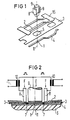
- FIG. 1 the positioning of the parts used during the method relative to a perpendicular axis 11 is shown in accordance with the method steps.
- An insulating film 3 with a working window 5 is positioned over a conductor track 4, which has a conductor track interruption 1 at a certain point, and again a molded part benefit 15 with at least one molded part 2, which is congruent with the conductor track interruption 1, is positioned over this insulating film 3.
- the exact alignment of the parts is given when the conductor interruption 1 appears in the center of the work window 5 and the molded part 2 is aligned congruently over the conductor interruption 1 and is symmetrically overlapping on both sides.
- connection process between the molded part 2 and the conductor track 4 can be carried out by means of the electron system 8; 9.
- this method provides a very specific advantage by holding the molded part 2 within the molded part benefit, in which between the process of aligning and lowering and the subsequent connection by means of resistance heating, no slipping of individual parts is possible.
- the main difference to previous methods is that the process of separating the corresponding molded part 2 from the Molded part 15 happens only after the connection process.
- the electrode system in this case a welding head with three electrodes 8; 9, is placed centrally on the molded part 2 in accordance with the axis 11.
- the position of the insulating film 3 is taken into account by the symmetrical position of the working window 5 with respect to the axis 11.
- the conductor track carrier 6 carries the conductor track 4, which has the conductor track interruption 1.
- the lenticular connection zones 7, which result from the connection by means of resistance heating, are placed approximately symmetrically with respect to the interruption in the conductor track 1 and arise where the spaces between the outer electrodes 8 and the inner electrode 9 are located.
- the inner electrode 9 is cylindrical and has lateral flats on the lower part, as is indicated in FIG. 1.
- the cross-section of the inner electrode 9 is adapted in accordance with the shape of the working window 5, which is also indicated in FIG. 1.
- This constructive measure also ensures protection of the adjacent conductor tracks, the spacing of which can be very small.
- the electrical supply to the electrode system 8; 9 is provided by two short-term energy sources 10, which are indicated in the form of transformers in FIG. 2. This provides short pulses, ideally vertical pulses, the current of which is, for example, 50 A with a voltage of 1 V and a pulse duration of 5 ms. Either hard soldering or welding can be carried out accordingly.
- the force F indicated in the figure, which is generated in each case by a spring, is a maximum of 0.6 N in the case of the inner electrode 9.
- the force on an outer electrode 8 is approximately one third or half of the force acting on the inner electrode 9 acts.
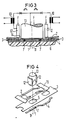
- FIG. 3 the same structure as in FIG. 2 is present with regard to the conductor track carrier 6, the conductor track 4, the insulating film 3 and the molded part 2.
- an electrode system 12; 13 is attached, which serves to separate out that section of the molded part 2 from the existing repair material that lies within the working window 5 and is connected to the conductor track 4.
- the outer electrodes 12 and the inner electrode 13 used in this case are dimensioned somewhat larger than the first electrode system 8; 9.
- the short-term energy sources 10, which are also used here, are decoupled by two diodes and give alternately, i.e. in succession, a short-term pulse.
- this second electrode system 12; 13 is also carried out centrally with respect to the axis 11 perpendicularly from above.
- the molded part 2 can be separated from the molded part benefit 15 at the edge of the working window 5 within the insulating film 3 by a described energy pulse.
- the separation point 14 is indicated in FIG. 3 between the left outer electrode 12 and the inner electrode 13. A time of approx. 300 ⁇ s is required for this separation process.
- the design of the electrode system has an impact on the quality of the separation process, with uniform separation with low energy expenditure being achievable by minimizing the distance between the outer electrodes 12 and the inner electrode 13 as far as possible.
- the mechanical control for positioning the individual parts is so precise that the coordinates of, for example, the axis 11 can be controlled precisely and the parts can be aligned accordingly.
- the method is monitored by means of optics, the use of a microscope being disadvantageous in that the free working space between the objective and the object is approximately 15 mm.
- the process is much easier to use if a CCD camera (Charged Coupled Device) is used.
- the height of the conductor track 4, the height of the insulating film 3 and the height of the molded part 2 are each 20 ⁇ m, for example. A range of approximately 40 ⁇ m depth can thus be observed from the surface of the molded part 2 to the surface of the conductor track 4.
- An above-mentioned camera has a depth of field of about 300 ⁇ m, thus fulfilling the optical accuracy and considerably facilitating the practical implementation of the method by the possibility of viewing the repair process on a screen.
- the advantage of using a three-electrode system as described lies in the double function of the respective inner electrode 9; 13. This is used in connection with an outer electrode 8, 12 in each case to produce a connection zone 7 or a separation point 14.
- the corresponding pulses from the short-term energy sources 10 are introduced at different times.
- controlled short-term energy sources are used, in which a target / actual value comparison for the control, i.e. ensures tracking.
- the temporal offset of the pulses between an outer electrode 8; 12 and the inner electrode 9; 13 is necessary so that the target / actual value recording is clear and there are no mutual falsifications.
- the material structure of a molded part 2 consists of a carrier layer, usually made of copper and a brazing layer usually applied by plating.
- the molded part 2 is placed on the conductor track 4 with a braze layer.
Abstract
Description
Die Erfindung betrifft ein Verfahren zur Reparatur von Fehlerstellen in Leiterbahnen, die mittels Überbrückung durch deckungsgleiche Formteile, die beiderseits des Fehlers gleichmäßig überlappend positioniert sind, behoben werden. Um eine elektrisch leitende und mechanisch tragende Verbindung herzustellen wird in der Regel eine Widerstandserwärmung, also eine Schweißung oder eine Hartlötung, hergestellt.The invention relates to a method for repairing fault locations in conductor tracks, which are remedied by bridging through congruent molded parts that are positioned uniformly overlapping on both sides of the fault. In order to establish an electrically conductive and mechanically load-bearing connection, resistance heating, i.e. welding or brazing, is generally carried out.
Die Weiterentwicklung von elektronischen Bauelementen und Leiterplatten geht einher mit einer Miniaturisierung der Leiterbahnen. Für die damit immer kostspieliger werdenden Leiterplatten, deren Leiterbahnen nach wie vor nicht fehlerfrei herstellbar sind, gewinnen entsprechende Reparaturverfahren zunehmend an Bedeutung. Die Forderungen an die Qualität derartiger Verfahren wächst ständig.The further development of electronic components and printed circuit boards goes hand in hand with miniaturization of the conductor tracks. Corresponding repair methods are becoming increasingly important for the circuit boards that are becoming ever more expensive and whose conductor tracks are still not flawlessly producible. The demands on the quality of such processes are constantly growing.
Bisherige Verfahren werden beispielsweise in der DE-PS 22 51 997 oder in der DE-OS 30 25 875 beschrieben. Hier werden zum einen hartlotplattierte Trägerbänder behandelt, die ausgestanzt, von einer Elektrode übernommen und auf die Fehlerstelle abgesenkt werden. Das deckungsgleiche Ausrichten geschieht durch optische Hilfsmittel. Die Nachteile der genannten Verfahren liegen zum einen in einer Vielzahl von Arbeitsschritten, wodurch ein Ausrichten und Positionieren eines Formteiles zur Reparatur einer defekten Leiterbahn erschwert wird, und zum anderen darin, daß durch die Miniaturisierung der heutigen Leiterbahnen, deren Breite mit ca. 50 bis 70 µm im Verhältnis zum Stand der Technik etwa halbiert wurde und deren Verlauf mäanderförmig ausgebildet ist, die Handhabung entsprechend kleiner Reparaturteile durch solche Verfahren nicht möglich ist.Previous methods are described for example in DE-PS 22 51 997 or in DE-OS 30 25 875. On the one hand, hard-soldered carrier tapes are treated, which are punched out, taken over by an electrode and lowered to the fault location. Alignment is done using optical aids. The disadvantages of the mentioned methods lie on the one hand in a large number of work steps, which makes alignment and positioning of a molded part for repairing a defective conductor track more difficult, and on the other hand in that the miniaturization of today's conductor tracks, the width of which is approximately 50 to 70 µm was about halved in relation to the prior art and the course of which is meandering, the handling of correspondingly small repair parts is not possible using such methods.
Der Erfindung liegt die Aufgabe zugrunde, ein Verfahren zur Reparatur von Leiterbahnenunterbrechungen durch Überbrückung mittels deckungsgleicher Formteile zur Verfügung zu stellen, mit dem in wenigen Arbeitsschritten ein Formteil deckungsgleich zur Leiterbahnunterbrechung und deren Umgebung ausgerichtet und mit der Leiterbahn mechanisch und elektrisch verbunden werden kann.The invention has for its object to provide a method for repairing conductor interruptions by bridging by means of congruent molded parts, with which a molded part can be aligned congruently with the interruption in the conductor path and its surroundings and mechanically and electrically connected to the conductor track.
Die Lösung dieser Aufgabe wird durch den kennzeichnenden Teil des Anspruches 1 wiedergegeben.The solution to this problem is given by the characterizing part of
Der Erfindung liegt die Erkenntnis zugrunde, daß der Vergleich zwischen Formteil und Leiterbahn zur Feststellung der Deckungsgleichheit und die Positionierung des Formteiles auf der Leiterbahn an der Stelle der Unterbrechung zur Einsparung von Arbeitsschritten am gleichen Ort geschehen muß. Hierzu wird ein Verband von einer Vielzahl von Formteilen, ein Formteilnutzen, verwendet, der nach dem Aufbringen einer Isolierfolie mit einem Arbeitsfenster auf der Leiterbahn derart über der Leiterbahnunterbrechung positioniert wird, daß durch Verfahren dieses Formteilnutzens relativ zur Leiterbahn bei gleichzeitiger Beobachtung durch eine Optik die Deckungsgleichheit zwischen Formteil und Leiterbahn festgestellt werden kann. Das Absenken des Formteiles mittels des Formteilnutzes auf die Leiterbahn kann ohne Zwischenschritte direkt geschehen. Der in Anschluß daran nötige Verbindungsvorgang durch Widerstandserwärmung und das Abtrennen des einen ausgewählten Formteiles aus dem Formteilnutzen geschehen durch jeweils ein Mehrfachelektrodensystem.The invention is based on the knowledge that the comparison between the molded part and the conductor track to determine the congruence and the positioning of the molded part on the conductor track at the point of the interruption to save work steps must be done at the same place. For this purpose, a bandage of a large number of molded parts, a molded part benefit, is used, which is positioned on the conductor track after the application of an insulating film with a working window on the conductor track in such a way that, by moving this molded part benefit relative to the conductor track while simultaneously observing through optics, the congruence can be determined between molded part and conductor track. The molded part can be lowered directly onto the conductor track by means of the molded part use without intermediate steps. The subsequent connection process by means of resistance heating and the separation of the one selected molded part from the molded part are done by a multiple electrode system.
Eine vorteilhafte Ausgestaltung der Erfindung sieht vor, daß innerhalb eines Formteilnutzen mehrere verschiedene Formteile entsprechend der auftretenden Leiterbahnkonfigurationen auf einer Leiterplatte enthalten sind. Dies vereinfacht ganz wesentlich den Vorgang des Vergleichens zwischen Formteilnutzen und Leiterbahn zur Auswahl eines deckungsgleichen Formteiles.An advantageous embodiment of the invention provides that within a molded part use several different molded parts are contained on a printed circuit board in accordance with the interconnect configurations that occur. This significantly simplifies the process of comparing the molded part benefit and the conductor track for the selection of a congruent molded part.
Zur Vermeidung eines paralaxen Fehlers bei der Auswahl und bei der deckungsgleichen Positionierung eines Formteiles bezüglich der Leiterbahnunterbrechung ist es vorteilhaft, diesen Vorgang senkrecht von oben zu kontrollieren.To avoid a paralax error in the selection and in the congruent positioning of a molded part the circuit break, it is advantageous to control this process vertically from above.
Diese Kontrolle kann mittels eines Mikroskopes geschehen, eine besonders vorteilhafte Ausführung sieht jedoch den Einsatz einer Fernsehkamera vor. Damit verbunden sind ganz wesentliche Vereinfachungen in der Handhabung bezüglich der Steuerung des Verfahrens.This control can be done using a microscope, but a particularly advantageous embodiment provides for the use of a television camera. Associated with this are very significant simplifications in handling with regard to the control of the process.
Zur einfachen und schnellen Durchführung des Verbindungsvorganges und des Trennvorganges ist der Einsatz von Elektrodensystemen, die mindestens drei Elektroden aufweisen, sehr vorteilhaft. Die Aufsetzflächen der Elektroden sind der Größe der Formteile, sowie der Größe der Arbeitsfenster innerhalb der Isolierfolie und dem Abstand der Leiterbahnen auf der Leiterplatte angepaßt und jede Elektrode ist für sich gefedert. Die Einzelelektroden eines Systemes sind weiterhin gegenseitig elektrisch getrennt, wodurch keinerlei Kurzschluß über das Formteil entstehen kann.The use of electrode systems which have at least three electrodes is very advantageous for the simple and quick implementation of the connection process and the separation process. The contact surfaces of the electrodes are adapted to the size of the molded parts and the size of the working window within the insulating film and the spacing of the conductor tracks on the circuit board, and each electrode is spring-loaded on its own. The individual electrodes of a system are also electrically isolated from one another, which means that no short circuit can occur across the molded part.
Die Materialauswahl bezüglich der Isolierfolie hat ergeben, daß eine Folie aus Polyimid für die in Frage kommenden thermischen, elektrischen und mechanischen Belastungen am besten geeignet ist. Eine derartige Folie ist bis zu 300° C temperaturbeständig.The choice of material with regard to the insulating film has shown that a film made of polyimide is best suited for the thermal, electrical and mechanical loads in question. Such a film is temperature resistant up to 300 ° C.
Zur Erzielung einer bezüglich der elektrischen und mechanischen Eigenschaften qualitativ guten Reparaturstelle ist es äußerst vorteilhaft, die thermische Belastung durch die Energieeinbringung bei der Widerstandserwärmung so gering wie möglich zu halten. Dies kann durch den Einsatz einer Kurzzeit-Energiequelle, die an die Elektrodensysteme angeschlossen ist, geschehen. Hierbei wird die Zeit der Widerstandserwärmung durch das Einbringen eines geregelten Kurzzeit-Impulses optimiert, d.h. so minimal wie möglich gehalten.In order to obtain a repair site that is of good quality with regard to the electrical and mechanical properties, it is extremely advantageous to keep the thermal load as a result of the energy input during resistance heating as low as possible. This can be done by using a short-term energy source that is connected to the electrode systems. The time of resistance heating is optimized by introducing a regulated short-term pulse, i.e. kept as minimal as possible.
Um eine Beschädigung der äußerst kleinen Leiterbahnen zu vermeiden, werden die einzeln gefederten Elektroden mit einer maximalen Kraft von 0,6 N angedrückt.To avoid damaging the extremely small conductor tracks, the individually sprung electrodes are covered with a maximum force of 0.6 N.
Im folgenden wird anhand von schematischen Zeichnungen ein Ausführungsbeispiel beschrieben:
- Fig. 1 zeigt die Relativlage von
Leiterbahnunterbrechung 1, Arbeitsfenster 5,Formteil 2 und Elektrodensystem 8;9. - Fig. 2 zeigt die Seitenansicht während des Verbindungsvorganges mittels des Elektrodensystems 8;9.
- Fig. 3 zeigt die Seitenansicht während des Trennvorganges mittels des
Elektrodensystems 12;13. - Fig. 4 zeigt die Realtivlage der verschiedenen Einheiten nach dem Reparaturvorgang.
- 1 shows the relative position of the
conductor interruption 1, working window 5, moldedpart 2 and electrode system 8; 9. - 2 shows the side view during the connection process by means of the electrode system 8; 9.
- 3 shows the side view during the separation process by means of the
electrode system 12; 13. - Fig. 4 shows the real situation of the various units after the repair process.
In der Fig. 1 ist entsprechend der Verfahrensschritte die Positionierung der während des Verfahrens eingesetzten Teile relativ zu einer senkrecht stehenden Achse 11 dargestellt. Über eine Leiterbahn 4, die an einer bestimmten Stelle eine Leiterbahnunterbrechung 1 aufweist, wird eine Isolierfolie 3 mit einem Arbeitsfenster 5 positioniert und wiederum über diese Isolierfolie 3 ein Formteilnutzen 15 mit mindestens einem Formteil 2, das deckungsgleich zur Leiterbahnunterbrechung 1 ist. Die genaue Ausrichtung der Teile ist gegeben, wenn die Leiterbahnunterbrechung 1 mittig im Arbeitsfenster 5 erscheint und das Formteil 2 deckungsgleich über der Leiterbahnunterbrechung 1 und zu dieser symmetrisch zu beiden Seiten überlappend ausgerichtet ist. Nach dem Absenken der Isolierfolie 3 und dem Formteilnutzen 15 mit dem Formteil 2 auf die Leiterbahn 4 kann der Verbindungsvorgang zwischen Formteil 2 und Leiterbahn 4 mittels des Elektronensystemes 8;9 vorgenommen werden. An dieser Stelle ist zu bemerken, daß dieses Verfahren einen ganz spezifischen Vorteil durch die Halterung des Formteiles 2 innerhalb des Formteilnutzens erbringt, in dem zwischen dem Vorgang des Ausrichtens und Absenkens und dem anschließenden Verbinden mittels Widerstandserwärmung kein Verrutschen einzelner Teile mehr möglich ist. Der wesentliche Unterschied zu bisherigen Verfahren besteht darin, daß der Vorgang des Heraustrennens des entsprechenden Formteiles 2 aus dem Formteilnutzen 15 erst nach dem Verbindungsvorgang geschieht.In FIG. 1, the positioning of the parts used during the method relative to a
Dieser Verbindungsvorgang wird durch die Anordnung der einzelnen Teile in der Fig. 2 dargestellt. Das Elektrodensystem, in diesem Fall ein Schweißkopf mit drei Elektroden 8;9 wird zentral entsprechend der Achse 11 auf dem Formteil 2 aufgesetzt. Die Lage der Isolierfolie 3 ist durch die symmetrische Lage des Arbeitsfensters 5 bezüglich der Achse 11 berücksichtigt. Der Leiterbahnträger 6 trägt die Leiterbahn 4, die die Leiterbahnunterbrechung 1 aufweist. Die linsenförmigen Verbindungszonen 7, die durch die Verbindung mittels Widerstandserwärmung entstehen sind annähernd symmetrisch zur Leiterbahnunterbrechung 1 plaziert und entstehen dort, wo sich die Zwischenräume zwischen den Außenelektroden 8 und der Innenelektrode 9 befinden. Die Innenelektrode 9 ist zylinderförmig ausgebildet und besitzt am unteren Teil seitliche Abflachungen, wie dies in der Fig. 1 angedeutet ist. Hierdurch wird der Aufsetzquerschnitt der Innenelektrode 9 entsprechend der ebenfalls in der Fig. 1 angedeuteten Form des Arbeitsfensters 5 angepaßt. Durch diese konstruktive Maßnahme wird außerdem ein Schutz der benachbarten Leiterbahnen, deren Abstände sehr gering sein können, gewährleistet. Die elektrische Versorgung des Elektrodensystems 8;9 geschieht durch zwei Kurzzeit-Energiequellen 10, die in der Fig. 2 in Form von Transformatoren angedeutet sind. Hierdurch werden kurze Impulse, im Idealfall Senkrechtimpulse geliefert, deren Stromstärke bei beispielsweise 50 A mit einer Spannung von 1 V und einer Impulsdauer von 5 ms liegt. Es kann wahlweise entsprechend eine Hartlötung oder eine Verschweißung durchgeführt werden. Die in der Figur angedeutete Kraft F, die jeweils durch eine Feder erzeugt wird, beträgt im Fall der Innenelektrode 9 maximal 0,6 N. Die Kraft an einer Außenelektrode 8 liegt etwa bei einem Drittel oder bei der Hälfte der Kraft, die auf die Innenelektrode 9 wirkt. Nach der Durchführung des Verbindungsvorganges wird das Elektrodensystem 8;9 entfernt.This connection process is shown by the arrangement of the individual parts in FIG. 2. The electrode system, in this case a welding head with three electrodes 8; 9, is placed centrally on the
In der Fig. 3 ist bezüglich des Leiterbahnträgers 6, der Leiterbahn 4, der Isolierfolie 3 und des Formteiles 2 der gleiche Aufbau wie in der Fig. 2 vorhanden. In diesem Fall ist jedoch ein Elektrodensystem 12;13 aufgesetzt, das zum Heraustrennen desjenigen Abschnittes des Formteiles 2 aus dem vorhandenen Reperaturmaterial dient, der innerhalb des Arbeitsfensters 5 liegt und mit der Leiterbahn 4 verbunden ist. Es ist deutlich zu erkennen, daß die in diesem Fall eingesetzten Außenelektroden 12 und die Innenelektrode 13 etwas größer dimensioniert sind, als das erste Elektrodensystem 8;9. Die Kurzzeit-Energiequellen 10, die hier ebenfalls zum Einsatz kommen, sind durch zwei Dioden entkoppelt und geben wechselweise, d.h. hintereinander, einen Kurzzeitimpuls ab. Die Ausrichtung dieses zweiten Elektrodensystemes 12;13 wird ebenfalls zentral bezüglich der Achse 11 senkrecht von oben her vorgenommen. Somit läßt sich das Formteil 2 an der Kante des Arbeitsfensters 5 innerhalb der Isolierfolie 3 durch einen beschriebenen Energieimpuls aus dem Formteilnutzen 15 heraustrennen. Die Trennstelle 14 ist in der Fig. 3 zwischen der linken Außenelektrode 12 und der Innenelektrode 13 angedeutet. Für diesen Trennvorgang ist eine Zeit von ca. 300 µs erforderlich. Die Auslegung des Elektrodensystemes hat Auswirkungen auf die Qualität des Trennvorganges, wobei eine gleichmäßige Trennung bei geringem Energieaufwand durch eine soweit als möglich vorgenommene Minimierung des Abstandes zwischen den Außenelektroden 12 und der Innenelektrode 13 erreichbar ist.In FIG. 3, the same structure as in FIG. 2 is present with regard to the
In der Fig. 4 sind sämtliche verfahrensrelevanten Teile relativ zur Achse 11 positioniert, wobei hier die ebenfalls senkrechte Stellung des zweiten Elektrodensystems 12;13 angedeutet ist. Das Formteil 2 innerhalb des Formteilnutzens 15 ist zu einem bestimmten benötigten Teil entsprechend der Dimensionierung des Arbeitsfensters 5 herausgetrennt worden und mit der Leiterbahn 4 verbunden worden. Hiermit lassen sich Unterbrechungen von bis zu 400 µm Länge reparieren.4, all process-relevant parts are positioned relative to the
Die mechanische Steuerung zur Positionierung der einzelnen Teile ist so präzise, daß die Koordinaten beispielsweise der Achse 11 genau angesteuert und die Teile entsprechend ausgerichtet werden können. Die Überwachung des Verfahrens erfolgt mittels einer Optik, wobei der Einsatz eines Mikroskopes insofern von Nachteil ist, als der freie Arbeitsraum zwischen Objektiv und Objekt bei ca. 15 mm liegt. Wesentlich einfacher zu handhaben ist das Verfahren, wenn eine CCD-Kamera (Charged Coupled Device) eingesetzt wird. Die Höhe der Leiterbahn 4, die Höhe der Isolierfolie 3 und die Höhe des Formteiles 2 betragen beispielsweise jeweils 20 µm. Somit ist ein Bereich von ca. 40 µm Tiefe von der Oberfläche des Formteiles 2 bis zur Oberfläche der Leiterbahn 4 zu beobachten. Eine oben erwähnte Kamera hat eine Schärfentiefe von etwa 300 µm, erfüllt somit die optische Genauigkeit und erleichtert durch die Möglichkeit der Betrachtung des Reparaturvorganges auf einem Bildschirm ganz wesentlich die praktische Durchführung des Verfahrens.The mechanical control for positioning the individual parts is so precise that the coordinates of, for example, the
Der Vorteil, ein beschriebenens Drei-Elektrodensystem einzusetzen liegt in der doppelten Funktion der jeweiligen Innenelektrode 9;13. Diese wird im Zusammenhang mit jeweils einer Außenelektrode 8;12 zur Herstellung jeweils einer Verbindungszone 7 oder einer Trennstelle 14 verwendet. Die entsprechenden Impulse der Kurzzeit-Energiequellen 10 werden zeitlich versetzt eingebracht. In diesem Fall werden geregelte Kurzzeit-Energiequellen verwendet, bei denen ein Soll/Ist-Wert-Vergleich für die Regelung, d.h. für eine Nachführung sorgt. Der zeitliche Versatz der Impulse zwischen jeweils einer Außenelektrode 8;12 und der Innenelektrode 9;13 ist notwendig, damit die Soll-/Istwertaufnahme eindeutig ist und keine gegenseitigen Verfälschungen vorkommen.The advantage of using a three-electrode system as described lies in the double function of the respective
Der materielle Aufbau eines Formteiles 2 besteht aus einer Trägerschicht, meist aus Kupfer und einer meist durch Plattierung aufgebrachten Hartlotschicht. Das Formteil 2 wird mit einer Hartlotschicht auf die Leiterbahn 4 aufgesetzt.The material structure of a molded
Claims (8)
dadurch gekennzeichnet,
daß
- eine Isolierfolie (3) mit einem Arbeitsfenster (5) derart auf die unterbrochene Leiterbahn (4) plaziert wird, daß die Leiterbahnunterbrechung (1) zumindest annähernd mittig im Arbeitsfenster (5) erscheint,
- ein in einem Formteilnutzen (15) gehaltenes zur Leiterbahnunterbrechung deckungsgleiches Formteil (2) durch Absenken des Formteilnutzens (15) auf die Isolierfolie (3) und die Leiterbahn (4) abgesenkt und gehalten wird,
- mit einem ersten Elektrodensystem (8;9) das Formteil (2) innerhalb des Arbeitsfensters (5) auf die Leiterbahn (4) gedrückt und beidseitig der Leiterbahnunterbrechung (1) mit der Leiterbahn (4) mechanisch und elektrisch verbunden wird,
- mit einem zweiten Elektrodensystem (12;13) die über das Arbeitsfenster (5) der Isolierfolie (3) hinausstehenden Teile des Formteiles (2) am Rand des Arbeitsfensters (5) mittels Widerstandserwärmung abgetrennt werden.1. Method for repairing conductor interruptions by bridging by means of congruent molded parts (2) and mutual connection by resistance heating,
characterized,
that
an insulating film (3) with a working window (5) is placed on the interrupted conductor track (4) in such a way that the conductor track interruption (1) appears at least approximately in the center of the working window (5),
a molded part (2) held in a molded part benefit (15) for interrupting the conductor track is lowered and held by lowering the molded part benefit (15) onto the insulating film (3) and the printed conductor (4),
- With a first electrode system (8; 9) the molded part (2) is pressed inside the working window (5) onto the conductor track (4) and mechanically and electrically connected to the conductor track (4) on both sides of the conductor track interruption (1),
- With a second electrode system (12; 13) which protrude beyond the working window (5) of the insulating film (3) parts of the molded part (2) at the edge of the working window (5) by means of resistance heating.
dadurch gekennzeichnet,
daß ein Formteil (2) aus verschiedenen Formteilnutzen ausgewählt wird, wobei die Formteilnutzen (15) mehrere verschiedenartige Formteile (2) entsprechend der auftretenden Leiterbahnkonfigurationen auf einer Leiterplatte enthalten.2. The method according to claim 1,
characterized,
that a molded part (2) is selected from different molded part benefits, wherein the molded part benefits (15) contain several different types of molded parts (2) according to the interconnect configurations occurring on a printed circuit board.
dadurch gekennzeichnet,
daß die Auswahl und deckungsgleiche Positionierung eines Formteiles (2) bezüglich der Leiterbahnunterbrechung (1) jeweils senkrecht von oben kontrolliert wird.3. The method according to any one of the preceding claims,
characterized,
that the selection and congruent positioning of a molded part (2) with respect to the circuit break (1) is checked vertically from above.
dadurch gekennzeichnet,
daß zur Auswahl und deckungsgleichen Positionierung eines Formteiles (2) bezüglich der Leiterbahnunterbrechung (1) eine Fernsehkamera verwendet wird.4. The method according to any one of the preceding claims,
characterized,
that a television camera is used for the selection and congruent positioning of a molded part (2) with respect to the circuit break (1).
dadurch gekennzeichnet,
daß als Elektrodensysteme Schweißköpfe mit mindestens drei Elektroden (8;9;12;13) eingesetzt werden, wobei jede Elektrode für sich gefedert ist und die Elektroden gegenseitig elektrisch getrennt sind.5. The method according to any one of the preceding claims,
characterized,
that welding heads with at least three electrodes (8; 9; 12; 13) are used as electrode systems, each electrode being spring-loaded and the electrodes being electrically separated from one another.
dadurch gekennzeichnet,
daß eine Isolierfolie (3) aus Polyimid verwendet wird.6. The method according to any one of the preceding claims,
characterized,
that an insulating film (3) made of polyimide is used.
dadurch gekennzeichnet,
daß die Energieversorgung der Elektrodensysteme (8;9;12;13) mittels Kurzzeit-Energiequellen (10) geschieht.7. The method according to any one of the preceding claims,
characterized,
that the energy supply to the electrode systems (8; 9; 12; 13) takes place by means of short-term energy sources (10).
dadurch gekennzeichnet,
daß die Andurckkräfte der Elektroden (8;9;12;13) maximal 0,6 N betragen.8. The method according to any one of the preceding claims,
characterized,
that the pressure forces of the electrodes (8; 9; 12; 13) are a maximum of 0.6 N.
Priority Applications (1)
| Application Number | Priority Date | Filing Date | Title |
|---|---|---|---|
| AT89107071T ATE59523T1 (en) | 1988-05-26 | 1989-04-19 | PROCEDURE FOR OPEN TRACK REPAIR. |
Applications Claiming Priority (2)
| Application Number | Priority Date | Filing Date | Title |
|---|---|---|---|
| DE3817900 | 1988-05-26 | ||
| DE3817900 | 1988-05-26 |
Publications (2)
| Publication Number | Publication Date |
|---|---|
| EP0343375A1 true EP0343375A1 (en) | 1989-11-29 |
| EP0343375B1 EP0343375B1 (en) | 1990-12-27 |
Family
ID=6355167
Family Applications (1)
| Application Number | Title | Priority Date | Filing Date |
|---|---|---|---|
| EP89107071A Expired - Lifetime EP0343375B1 (en) | 1988-05-26 | 1989-04-19 | Method for cancelling of conductive-path interruptions |
Country Status (4)
| Country | Link |
|---|---|
| US (1) | US4908938A (en) |
| EP (1) | EP0343375B1 (en) |
| AT (1) | ATE59523T1 (en) |
| DE (1) | DE58900037D1 (en) |
Cited By (1)
| Publication number | Priority date | Publication date | Assignee | Title |
|---|---|---|---|---|
| EP3799522A1 (en) * | 2019-09-26 | 2021-03-31 | Georg Emeis | Method and device for electrical resistance heating |
Families Citing this family (14)
| Publication number | Priority date | Publication date | Assignee | Title |
|---|---|---|---|---|
| US5120924A (en) * | 1990-05-16 | 1992-06-09 | Akio Hirane | Welding method for coated metal articles |
| US5060370A (en) * | 1990-10-15 | 1991-10-29 | Scales Jr James W | Modification method for etched printed circuit boards |
| US5288007A (en) * | 1991-10-04 | 1994-02-22 | International Business Machine Corporation | Apparatus and methods for making simultaneous electrical connections |
| US5243140A (en) * | 1991-10-04 | 1993-09-07 | International Business Machines Corporation | Direct distribution repair and engineering change system |
| US5193732A (en) * | 1991-10-04 | 1993-03-16 | International Business Machines Corporation | Apparatus and methods for making simultaneous electrical connections |
| US5289632A (en) * | 1992-11-25 | 1994-03-01 | International Business Machines Corporation | Applying conductive lines to integrated circuits |
| US5384953A (en) * | 1993-07-21 | 1995-01-31 | International Business Machines Corporation | Structure and a method for repairing electrical lines |
| US5904868A (en) * | 1994-06-16 | 1999-05-18 | International Business Machines Corporation | Mounting and/or removing of components using optical fiber tools |
| US6035526A (en) * | 1997-11-18 | 2000-03-14 | Ntn Corporation | Method of repairing defect and apparatus for repairing defect |
| US6651322B1 (en) * | 2000-12-28 | 2003-11-25 | Unisys Corporation | Method of reworking a multilayer printed circuit board assembly |
| EP1577046B1 (en) * | 2004-03-18 | 2009-11-25 | Augusto Vincenzi | Method and device for fixing a functional member to a surface |
| WO2012043587A1 (en) * | 2010-09-30 | 2012-04-05 | 本田技研工業株式会社 | Welding device |
| US8870051B2 (en) * | 2012-05-03 | 2014-10-28 | International Business Machines Corporation | Flip chip assembly apparatus employing a warpage-suppressor assembly |
| US20190366460A1 (en) * | 2018-06-01 | 2019-12-05 | Progress Y&Y Corp. | Soldering apparatus and solder nozzle module thereof |
Citations (1)
| Publication number | Priority date | Publication date | Assignee | Title |
|---|---|---|---|---|
| EP0043586A2 (en) * | 1980-07-08 | 1982-01-13 | Siemens Aktiengesellschaft | Means for repairing ruptures of conductors on a printed-circuit board |
Family Cites Families (5)
| Publication number | Priority date | Publication date | Assignee | Title |
|---|---|---|---|---|
| DE2251997C3 (en) * | 1972-10-24 | 1985-03-14 | Siemens AG, 1000 Berlin und 8000 München | Method for repairing narrow conductor tracks in electrical circuit boards |
| US3964666A (en) * | 1975-03-31 | 1976-06-22 | Western Electric Company, Inc. | Bonding contact members to circuit boards |
| US4259367A (en) * | 1979-07-30 | 1981-03-31 | International Business Machines Corporation | Fine line repair technique |
| GB2067845B (en) * | 1980-01-23 | 1984-04-26 | Int Computers Ltd | Manufacture of printed circuit boards |
| US4808157A (en) * | 1987-07-13 | 1989-02-28 | Neuro Delivery Technology, Inc. | Multi-lumen epidural-spinal needle |
-
1989
- 1989-03-23 US US07/327,907 patent/US4908938A/en not_active Expired - Fee Related
- 1989-04-19 AT AT89107071T patent/ATE59523T1/en not_active IP Right Cessation
- 1989-04-19 DE DE8989107071T patent/DE58900037D1/en not_active Expired - Fee Related
- 1989-04-19 EP EP89107071A patent/EP0343375B1/en not_active Expired - Lifetime
Patent Citations (1)
| Publication number | Priority date | Publication date | Assignee | Title |
|---|---|---|---|---|
| EP0043586A2 (en) * | 1980-07-08 | 1982-01-13 | Siemens Aktiengesellschaft | Means for repairing ruptures of conductors on a printed-circuit board |
Non-Patent Citations (2)
| Title |
|---|
| DESIGN ENGINEERING, Band 51, Nr. 4, Oktober 1980, Seite 23, Waseca, US; "A high-speed soldering system" * |
| IBM TECHNICAL DISCLOSURE BULLETIN, Band 14, Nr. 10, März 1972, Seite 2915, New York, US; F.M. TAPPEN: "Open conductor repair for glass metal module" * |
Cited By (1)
| Publication number | Priority date | Publication date | Assignee | Title |
|---|---|---|---|---|
| EP3799522A1 (en) * | 2019-09-26 | 2021-03-31 | Georg Emeis | Method and device for electrical resistance heating |
Also Published As
| Publication number | Publication date |
|---|---|
| ATE59523T1 (en) | 1991-01-15 |
| EP0343375B1 (en) | 1990-12-27 |
| US4908938A (en) | 1990-03-20 |
| DE58900037D1 (en) | 1991-02-07 |
Similar Documents
| Publication | Publication Date | Title |
|---|---|---|
| EP0343375B1 (en) | Method for cancelling of conductive-path interruptions | |
| EP0285799B1 (en) | Device for the functional electric testing of wiring arrays, in particular of circuit boards | |
| DE2152081C2 (en) | Process for mounting integrated circuit chips on an insulating substrate | |
| DE3011465C2 (en) | Spark gap on a circuit board | |
| DE3902158A1 (en) | METHOD FOR REMOVING AN INSULATING COVER OF AN ELECTRICAL LINE WIRE, AND DEVICE FOR IMPLEMENTING THE METHOD | |
| DE2319011A1 (en) | METHOD OF EECTRIC TESTING A CHIP CONNECTING CIRCUIT NETWORK ON A SUBSTRATE | |
| DE1950516B2 (en) | CONNECTION ELECTRIC CONDUCTORS | |
| DE3510961C2 (en) | ||
| DE112004000434B4 (en) | Electrostatic levitation furnace and method for melting samples using the furnace | |
| EP0343374B1 (en) | Method of cancelling interruptions in conducting paths by means of a congruent element | |
| DE4302509B4 (en) | Method for testing circuit boards | |
| EP0285798A2 (en) | Device for the functional electric testing of wiring arrays, in particular of circuit boards | |
| EP0322607B1 (en) | Control device for an apparatus for testing electrical function of wiring patterns | |
| DE3035970C2 (en) | Method for adjusting the electrode spacing in beam generation systems of cathode ray tubes | |
| DE3218849C2 (en) | ||
| DE2259133C3 (en) | Method for contacting a semiconductor arrangement and application of the method | |
| DE2812976C2 (en) | Method for determining the offset between conductor tracks and contact holes in a circuit board and a circuit board for use in this method | |
| DE3008685A1 (en) | METHOD AND DEVICE FOR ADJUSTING THE FREQUENCY CHARACTERISTICS OF A PIEZOELECTRIC RESONATOR | |
| DE2942056C2 (en) | In-line electron gun | |
| DE3216041C2 (en) | ||
| DE3313456C2 (en) | Impulse soldering process | |
| EP0286814A2 (en) | Addressing device | |
| DE3102183C2 (en) | Electron beam system for television picture tubes | |
| DE3138285A1 (en) | Supporting plate which can be plugged vertically onto a printed-circuit board by means of a plurality of rows of conductive pins, and a method for producing the supporting plate | |
| EP0068493A1 (en) | Contact probe assembly for integrated circuits |
Legal Events
| Date | Code | Title | Description |
|---|---|---|---|
| PUAI | Public reference made under article 153(3) epc to a published international application that has entered the european phase |
Free format text: ORIGINAL CODE: 0009012 |
|
| AK | Designated contracting states |
Kind code of ref document: A1 Designated state(s): AT BE CH DE FR GB IT LI NL |
|
| 17P | Request for examination filed |
Effective date: 19900110 |
|
| 17Q | First examination report despatched |
Effective date: 19900605 |
|
| GRAA | (expected) grant |
Free format text: ORIGINAL CODE: 0009210 |
|
| AK | Designated contracting states |
Kind code of ref document: B1 Designated state(s): AT BE CH DE FR GB IT LI NL |
|
| REF | Corresponds to: |
Ref document number: 59523 Country of ref document: AT Date of ref document: 19910115 Kind code of ref document: T |
|
| REF | Corresponds to: |
Ref document number: 58900037 Country of ref document: DE Date of ref document: 19910207 |
|
| ET | Fr: translation filed | ||
| ITF | It: translation for a ep patent filed |
Owner name: STUDIO JAUMANN |
|
| GBT | Gb: translation of ep patent filed (gb section 77(6)(a)/1977) | ||
| ITTA | It: last paid annual fee | ||
| PGFP | Annual fee paid to national office [announced via postgrant information from national office to epo] |
Ref country code: CH Payment date: 19910724 Year of fee payment: 3 |
|
| PLBE | No opposition filed within time limit |
Free format text: ORIGINAL CODE: 0009261 |
|
| STAA | Information on the status of an ep patent application or granted ep patent |
Free format text: STATUS: NO OPPOSITION FILED WITHIN TIME LIMIT |
|
| 26N | No opposition filed | ||
| PGFP | Annual fee paid to national office [announced via postgrant information from national office to epo] |
Ref country code: AT Payment date: 19920327 Year of fee payment: 4 |
|
| PGFP | Annual fee paid to national office [announced via postgrant information from national office to epo] |
Ref country code: FR Payment date: 19920428 Year of fee payment: 4 Ref country code: BE Payment date: 19920428 Year of fee payment: 4 |
|
| PG25 | Lapsed in a contracting state [announced via postgrant information from national office to epo] |
Ref country code: LI Effective date: 19920430 Ref country code: CH Effective date: 19920430 |
|
| PGFP | Annual fee paid to national office [announced via postgrant information from national office to epo] |
Ref country code: NL Payment date: 19920430 Year of fee payment: 4 |
|
| REG | Reference to a national code |
Ref country code: CH Ref legal event code: PL |
|
| PG25 | Lapsed in a contracting state [announced via postgrant information from national office to epo] |
Ref country code: GB Effective date: 19930419 Ref country code: AT Effective date: 19930419 |
|
| PG25 | Lapsed in a contracting state [announced via postgrant information from national office to epo] |
Ref country code: BE Effective date: 19930430 |
|
| BERE | Be: lapsed |
Owner name: SIEMENS A.G. Effective date: 19930430 |
|
| PG25 | Lapsed in a contracting state [announced via postgrant information from national office to epo] |
Ref country code: NL Effective date: 19931101 |
|
| GBPC | Gb: european patent ceased through non-payment of renewal fee |
Effective date: 19930419 |
|
| NLV4 | Nl: lapsed or anulled due to non-payment of the annual fee | ||
| PG25 | Lapsed in a contracting state [announced via postgrant information from national office to epo] |
Ref country code: FR Effective date: 19931229 |
|
| REG | Reference to a national code |
Ref country code: FR Ref legal event code: ST |
|
| PGFP | Annual fee paid to national office [announced via postgrant information from national office to epo] |
Ref country code: DE Payment date: 19960620 Year of fee payment: 8 |
|
| PG25 | Lapsed in a contracting state [announced via postgrant information from national office to epo] |
Ref country code: DE Free format text: LAPSE BECAUSE OF NON-PAYMENT OF DUE FEES Effective date: 19980101 |
|
| PG25 | Lapsed in a contracting state [announced via postgrant information from national office to epo] |
Ref country code: IT Free format text: LAPSE BECAUSE OF NON-PAYMENT OF DUE FEES;WARNING: LAPSES OF ITALIAN PATENTS WITH EFFECTIVE DATE BEFORE 2007 MAY HAVE OCCURRED AT ANY TIME BEFORE 2007. THE CORRECT EFFECTIVE DATE MAY BE DIFFERENT FROM THE ONE RECORDED. Effective date: 20050419 |