EP0343374B1 - Method of cancelling interruptions in conducting paths by means of a congruent element - Google Patents
Method of cancelling interruptions in conducting paths by means of a congruent element Download PDFInfo
- Publication number
- EP0343374B1 EP0343374B1 EP89107047A EP89107047A EP0343374B1 EP 0343374 B1 EP0343374 B1 EP 0343374B1 EP 89107047 A EP89107047 A EP 89107047A EP 89107047 A EP89107047 A EP 89107047A EP 0343374 B1 EP0343374 B1 EP 0343374B1
- Authority
- EP
- European Patent Office
- Prior art keywords
- conductor path
- interruption
- conductor
- shaped element
- conformal
- Prior art date
- Legal status (The legal status is an assumption and is not a legal conclusion. Google has not performed a legal analysis and makes no representation as to the accuracy of the status listed.)
- Expired - Lifetime
Links
- 238000000034 method Methods 0.000 title claims abstract description 22
- 239000004020 conductor Substances 0.000 claims abstract description 70
- 238000010438 heat treatment Methods 0.000 claims description 7
- 230000008439 repair process Effects 0.000 abstract description 4
- 238000012544 monitoring process Methods 0.000 abstract 1
- 230000008569 process Effects 0.000 description 7
- 238000004080 punching Methods 0.000 description 5
- PXHVJJICTQNCMI-UHFFFAOYSA-N Nickel Chemical compound [Ni] PXHVJJICTQNCMI-UHFFFAOYSA-N 0.000 description 4
- 239000000463 material Substances 0.000 description 3
- RYGMFSIKBFXOCR-UHFFFAOYSA-N Copper Chemical compound [Cu] RYGMFSIKBFXOCR-UHFFFAOYSA-N 0.000 description 2
- 239000000956 alloy Substances 0.000 description 2
- 229910045601 alloy Inorganic materials 0.000 description 2
- 230000008901 benefit Effects 0.000 description 2
- 238000005219 brazing Methods 0.000 description 2
- 238000000465 moulding Methods 0.000 description 2
- 229910052759 nickel Inorganic materials 0.000 description 2
- 239000012876 carrier material Substances 0.000 description 1
- 230000008859 change Effects 0.000 description 1
- 238000007796 conventional method Methods 0.000 description 1
- 229910052802 copper Inorganic materials 0.000 description 1
- 239000010949 copper Substances 0.000 description 1
- 238000005520 cutting process Methods 0.000 description 1
- 230000007547 defect Effects 0.000 description 1
- 238000007747 plating Methods 0.000 description 1
- 238000003860 storage Methods 0.000 description 1
- 238000003466 welding Methods 0.000 description 1
Images
Classifications
-
- H—ELECTRICITY
- H05—ELECTRIC TECHNIQUES NOT OTHERWISE PROVIDED FOR
- H05K—PRINTED CIRCUITS; CASINGS OR CONSTRUCTIONAL DETAILS OF ELECTRIC APPARATUS; MANUFACTURE OF ASSEMBLAGES OF ELECTRICAL COMPONENTS
- H05K3/00—Apparatus or processes for manufacturing printed circuits
- H05K3/22—Secondary treatment of printed circuits
- H05K3/225—Correcting or repairing of printed circuits
-
- H—ELECTRICITY
- H05—ELECTRIC TECHNIQUES NOT OTHERWISE PROVIDED FOR
- H05K—PRINTED CIRCUITS; CASINGS OR CONSTRUCTIONAL DETAILS OF ELECTRIC APPARATUS; MANUFACTURE OF ASSEMBLAGES OF ELECTRICAL COMPONENTS
- H05K1/00—Printed circuits
- H05K1/02—Details
- H05K1/0266—Marks, test patterns or identification means
- H05K1/0269—Marks, test patterns or identification means for visual or optical inspection
-
- H—ELECTRICITY
- H05—ELECTRIC TECHNIQUES NOT OTHERWISE PROVIDED FOR
- H05K—PRINTED CIRCUITS; CASINGS OR CONSTRUCTIONAL DETAILS OF ELECTRIC APPARATUS; MANUFACTURE OF ASSEMBLAGES OF ELECTRICAL COMPONENTS
- H05K2201/00—Indexing scheme relating to printed circuits covered by H05K1/00
- H05K2201/10—Details of components or other objects attached to or integrated in a printed circuit board
- H05K2201/10227—Other objects, e.g. metallic pieces
- H05K2201/1028—Thin metal strips as connectors or conductors
-
- H—ELECTRICITY
- H05—ELECTRIC TECHNIQUES NOT OTHERWISE PROVIDED FOR
- H05K—PRINTED CIRCUITS; CASINGS OR CONSTRUCTIONAL DETAILS OF ELECTRIC APPARATUS; MANUFACTURE OF ASSEMBLAGES OF ELECTRICAL COMPONENTS
- H05K2203/00—Indexing scheme relating to apparatus or processes for manufacturing printed circuits covered by H05K3/00
- H05K2203/11—Treatments characterised by their effect, e.g. heating, cooling, roughening
- H05K2203/1115—Resistance heating, e.g. by current through the PCB conductors or through a metallic mask
-
- H—ELECTRICITY
- H05—ELECTRIC TECHNIQUES NOT OTHERWISE PROVIDED FOR
- H05K—PRINTED CIRCUITS; CASINGS OR CONSTRUCTIONAL DETAILS OF ELECTRIC APPARATUS; MANUFACTURE OF ASSEMBLAGES OF ELECTRICAL COMPONENTS
- H05K2203/00—Indexing scheme relating to apparatus or processes for manufacturing printed circuits covered by H05K3/00
- H05K2203/16—Inspection; Monitoring; Aligning
- H05K2203/166—Alignment or registration; Control of registration
-
- H—ELECTRICITY
- H05—ELECTRIC TECHNIQUES NOT OTHERWISE PROVIDED FOR
- H05K—PRINTED CIRCUITS; CASINGS OR CONSTRUCTIONAL DETAILS OF ELECTRIC APPARATUS; MANUFACTURE OF ASSEMBLAGES OF ELECTRICAL COMPONENTS
- H05K2203/00—Indexing scheme relating to apparatus or processes for manufacturing printed circuits covered by H05K3/00
- H05K2203/17—Post-manufacturing processes
- H05K2203/173—Adding connections between adjacent pads or conductors, e.g. for modifying or repairing
-
- H—ELECTRICITY
- H05—ELECTRIC TECHNIQUES NOT OTHERWISE PROVIDED FOR
- H05K—PRINTED CIRCUITS; CASINGS OR CONSTRUCTIONAL DETAILS OF ELECTRIC APPARATUS; MANUFACTURE OF ASSEMBLAGES OF ELECTRICAL COMPONENTS
- H05K3/00—Apparatus or processes for manufacturing printed circuits
- H05K3/30—Assembling printed circuits with electric components, e.g. with resistor
- H05K3/32—Assembling printed circuits with electric components, e.g. with resistor electrically connecting electric components or wires to printed circuits
- H05K3/328—Assembling printed circuits with electric components, e.g. with resistor electrically connecting electric components or wires to printed circuits by welding
-
- Y—GENERAL TAGGING OF NEW TECHNOLOGICAL DEVELOPMENTS; GENERAL TAGGING OF CROSS-SECTIONAL TECHNOLOGIES SPANNING OVER SEVERAL SECTIONS OF THE IPC; TECHNICAL SUBJECTS COVERED BY FORMER USPC CROSS-REFERENCE ART COLLECTIONS [XRACs] AND DIGESTS
- Y10—TECHNICAL SUBJECTS COVERED BY FORMER USPC
- Y10T—TECHNICAL SUBJECTS COVERED BY FORMER US CLASSIFICATION
- Y10T29/00—Metal working
- Y10T29/49—Method of mechanical manufacture
- Y10T29/49002—Electrical device making
- Y10T29/49117—Conductor or circuit manufacturing
- Y10T29/49124—On flat or curved insulated base, e.g., printed circuit, etc.
- Y10T29/49155—Manufacturing circuit on or in base
-
- Y—GENERAL TAGGING OF NEW TECHNOLOGICAL DEVELOPMENTS; GENERAL TAGGING OF CROSS-SECTIONAL TECHNOLOGIES SPANNING OVER SEVERAL SECTIONS OF THE IPC; TECHNICAL SUBJECTS COVERED BY FORMER USPC CROSS-REFERENCE ART COLLECTIONS [XRACs] AND DIGESTS
- Y10—TECHNICAL SUBJECTS COVERED BY FORMER USPC
- Y10T—TECHNICAL SUBJECTS COVERED BY FORMER US CLASSIFICATION
- Y10T29/00—Metal working
- Y10T29/49—Method of mechanical manufacture
- Y10T29/49718—Repairing
- Y10T29/49732—Repairing by attaching repair preform, e.g., remaking, restoring, or patching
- Y10T29/49742—Metallurgically attaching preform
Definitions
- the invention relates to a method for repairing conductor interruptions by means of congruent molded parts, these being connected to the conductor path on both sides of the conductor interruptions by means of resistance heating.
- This relates specifically to conductor tracks, the height of which is, for example, 20 to 30 ⁇ m and the width of which is approximately 50 to 70 ⁇ m.
- a method for repairing conductor interruptions is already known from DE-OS 3025875, which corresponds to EP-A-0043586.
- a three-part electrode system is used, which consists of a central inner electrode equipped with a vacuum connection for sucking in a molded part, and which, by means of concentrically and semicircularly arranged outer electrodes, serves overall to receive a molded part, to deposit it and to connect this molded part to the interrupted conductor track.
- a braze joint is generally used for the connection by means of resistance heating.
- DE-PS 2251997 discloses material and welding data relating to such a braze joint.
- the invention has for its object to provide a method for repairing interruptions in the conductor that the congruent moldings required to the area of Selects and interrupts the conductor interruption and symmetrically to it, and places it on the conductor interruption for connection by means of resistance heating.
- the invention is based on the knowledge that the reliable handling of molded parts for repairing conductor interruptions, based on their congruence and alignment with respect to the conductor trace, is only possible by means of a television camera at the locations of the conductor interruption, the selection of a molded part and the location of the connection between Molding and trace, can be realized.
- the three black and white television pictures available in this way are each placed on a color input on a color monitor and can be mixed to ensure very precise control of the congruence. This happens through a color change, which marks the moment of congruence of two black and white pictures, each of which previously had its own color and different from the other picture. If they are congruent, a third, new color appears in the overlapping area.
- a particularly advantageous embodiment of the invention provides for the use of a three-part electrode head which, by means of a central, rotatable suction electrode, picks up the molded part, aligns it by rotating it relative to the interruption in the conductor track, and positions it thereon.
- a three-part electrode head which, by means of a central, rotatable suction electrode, picks up the molded part, aligns it by rotating it relative to the interruption in the conductor track, and positions it thereon.
- the molded parts required for different conductor track geometries are expediently kept available in a storage device in order to feed them to a punching tool, the suction electrode removing the punched-out molded part directly from the Removes punch.
- the three outputs of the three black / white television cameras connected to a color monitor can advantageously be coordinated in such a way that the first television camera constantly occupies one input and either the second or the third television camera alternately occupy a second common input. This has the advantage that the third color input is available for another television camera and additional control functions.
- a second solution to the above object is given by the characterizing part of claim 6.
- This second solution which is based on the same principle of the invention, provides for the exchange of the first and the second as well as the first and the third television camera in each case by a comparison microscope which compares two images accordingly.
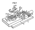
- the television cameras 1 to 4 are shown.
- the first television camera 1 and the second television camera 2 on the one hand capture the printed circuit board 19 with an interruption in the conductor track and on the other hand a magazine 9, in this case a round magazine, with a punching tool 18. In both cases this is done vertically from above.
- the camera 3 looks vertically from below the three-part electrode head 6 with the rotatable suction electrode 5.
- the camera 4 looks obliquely from the side at the place where the connection is made by resistance heating between the molded part 11 and the conductor track 10. This coincides with the position above the television camera 3.
- the device mounted on a stand 7 also consists of a sliding table 8 which can be moved back and forth in one direction by means of a stepping motor 36.
- the relevant movement is necessary in order to move the stamping tool 18 with the magazine 9 and the printed circuit board 19 from the position shown in each case under the three-part electrode head 6 with the rotatable suction electrode 5.
- the stepper motors 30; 31; 32 ensure a rough and fine adjustment of the printed circuit board 19 with respect to a zero point fixed on the color monitor 16.
- the stepper motor 35 is responsible for the movements of the punch 18.
- the stepper motors 38; 37 move the electrode head 6 and the separately rotatable suction electrode 5.
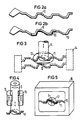
- FIG. 2a shows a conductor track 10 which has a defect in the form of an interruption.
- FIG. 2b shows a molded part 11 which is congruent with the area around the conductor track interruption and bridges or overlaps approximately equally on both sides, which was positioned on the conductor track and was electrically and mechanically connected to the conductor track 10 by two connection zones 20 by means of brazing.
- FIG. 3 shows an example of how a molded part 14, which contains a plurality of molded parts 11, is made by means of the vertically removable and separately rotatable suction electrode 5, the stamping punch 13, of which only the base area is shown and a shaped part 11 is punched out of the cutting plate opening 12 and is sucked in by means of a vacuum.
- double arrows show the directions in which the suction electrode 5 and the outer electrodes 15 can be moved.
- the electrodes 5; 15 are each movable in ball guides and spring-loaded.
- the suction electrode 5 protrudes downward centrally from the pair of the outer electrodes 15, since it has to remove the molded part 11 from the stamping tool 18 at a time in which the outer electrodes 15 are not used.
- the connection process between the molded part 11 and the conductor track 10 takes place by fitting all three electrodes, a resistance welded or brazed connection being produced approximately symmetrically to the conductor track interruption in each case between the suction electrode 5 and the outer electrodes 15.
- FIG. 5 indicates how a color trace 16 is used to repair a conductor track 10, the conductor track interruption of which is approximately in the crosshairs 17, by means of a molded part 11.
- the crosshair 17 represents the reference point for the position recorded with a camera in each case. Using this reference point, the conductor interruption can be recorded centrally on the color monitor 16, as can the molded part 11, which is symmetrical, i.e. is positioned on both sides evenly overlapping to interrupt the conductor track.
- the only time that is not by means of one of the cameras 1; 2; 3 can be detected, namely the connection process by means of resistance heating, can be observed by the camera 4 obliquely from the side.
- All stepper motors are designed according to the dimensioning of the conductor tracks and the repair molded parts so that the congruence can be set exactly when comparing several images.
- the orientation of the third television camera 3 is selected such that the molded part 11 held by the suction electrode 5 can be positioned congruently and, after the circuit board 19 has been moved under the suction electrode, can be lowered correspondingly onto the conductor track.
- microscopes can also be used in some cases. It is advisable to use comparison microscopes (two objectives, one eyepiece). Comparison microscopes can expediently instead of the first and the second television camera 1; 2, and instead of the first and third television cameras 1; 3 are used. Instead of the fourth television camera 4, an obliquely arranged stereo microscope can be used be directed directly to the interruption of the conductor track 10.
Landscapes
- Engineering & Computer Science (AREA)
- Manufacturing & Machinery (AREA)
- Microelectronics & Electronic Packaging (AREA)
- Manufacturing Of Printed Wiring (AREA)
- Investigating Materials By The Use Of Optical Means Adapted For Particular Applications (AREA)
- Length Measuring Devices By Optical Means (AREA)
Abstract
Description
Die Erfindung betrifft ein Verfahren zur Reparatur von Leiterbahnunterbrechungen mittels deckungsgleicher Formteile, wobei diese beiderseits der Leiterbahnunterbrechungen mittels Widerstandserwärmung mit der Leiterbahn verbunden werden. Dies bezieht sich speziell auf Leiterbahnen, deren Höhe beispielsweise 20 bis 30 µm und deren Breite ca. 50 bis 70 µm beträgt.The invention relates to a method for repairing conductor interruptions by means of congruent molded parts, these being connected to the conductor path on both sides of the conductor interruptions by means of resistance heating. This relates specifically to conductor tracks, the height of which is, for example, 20 to 30 µm and the width of which is approximately 50 to 70 µm.
Ein Verfahren zur Reparatur von Leiterbahnunterbrechungen ist bereits aus der DE-OS 3025875, die der EP-A-0043586 entspricht, bekannt. Hierin wird ein dreiteiliges Elektrodensystem verwendet, das aus einer zentrischen mit einem Vakuumanschluß zum Ansaugen eines Formteiles ausgestatteten Innenelektrode besteht, und das mittels konzentrisch und halbkreisförmig angeordneter Außenelektroden insgesamt zum Aufnehmen eines Formteiles, zum Absetzen desselben und zum Verbinden dieses Formteiles mit der unterbrochenen Leiterbahn dient. Zur Verbindung mittels Widerstandserwärmung wird in der Regel eine Hartlötverbindung eingesetzt. In der DE-PS 2251997 werden werkstoffkundliche und schweißtechnische Daten bezüglich einer solchen Hartlotverbindung offenbart.A method for repairing conductor interruptions is already known from DE-OS 3025875, which corresponds to EP-A-0043586. Herein, a three-part electrode system is used, which consists of a central inner electrode equipped with a vacuum connection for sucking in a molded part, and which, by means of concentrically and semicircularly arranged outer electrodes, serves overall to receive a molded part, to deposit it and to connect this molded part to the interrupted conductor track. A braze joint is generally used for the connection by means of resistance heating. DE-PS 2251997 discloses material and welding data relating to such a braze joint.
Bei der weiter fortschreitenden Miniaturisierung von Leiterbahnen, die mittlerweile mäanderförmig in trapezartigen Leiterbahnzügen verlaufen und Dimensionierungen mit beispielsweise weniger als 70 µm Breite besitzen, sind Reparaturen an entsprechenden Leiterplatten mit herkömmlichen Verfahren nicht durchführbar. Dies ist im wesentlichen auf die mit dem menschlichen Auge nicht mehr zu verwirklichende Kontrolle bei den beschriebenen Dimensionen zurückzuführen.With the advancing miniaturization of conductor tracks, which now run in a meandering shape in trapezoidal conductor tracks and have dimensions of less than 70 µm, for example, repairs to corresponding circuit boards cannot be carried out using conventional methods. This is essentially due to the control of the dimensions described that can no longer be carried out with the human eye.
Der Erfindung liegt die Aufgabe zugrunde, ein Verfahren zur Reparatur von Leiterbahnunterbrechungen bereitzustellen, das die dazu benötigten Formteile deckungsgleich zum Bereich der Leiterbahnunterbrechung und symmetrisch zu dieser auswählt, aufnimmt und zur Verbindung mittels Widerstandserwärmung entsprechend auf die Leiterbahnunterbrechung absetzt.The invention has for its object to provide a method for repairing interruptions in the conductor that the congruent moldings required to the area of Selects and interrupts the conductor interruption and symmetrically to it, and places it on the conductor interruption for connection by means of resistance heating.
Die Lösung dieser Aufgabe wird durch den kennzeichnenden Teil des Anspruches 1 wiedergegeben.The solution to this problem is given by the characterizing part of claim 1.
Der Erfindung liegt die Erkenntnis zugrunde, daß die zuverlässige Handhabung von Formteilen zur Reparatur von Leiterbahnunterbrechungen, bezogen auf deren Deckungsgleichheit und Ausrichtung bezüglich der Leiterbahn, nur durch die Erfassung mittels Fernsehkamera an den Stellen der Leiterbahnunterbrechung, der Auswahl eines Formteiles und des Ortes der Verbindung zwischen Formteil und Leiterbahn, verwirklicht werden kann. Die dadurch erhältlichen drei Schwarz/Weiß-Fernsehbilder werden auf jeweils einen Farb-Eingang eines Farbmonitors gelegt und können durch wahlweises Mischen eine sehr exakte Kontrolle der Deckungsgleichheit gewährleisten. Dies geschieht durch einen Farbumschlag, der den Moment der Deckungsgleichheit zweier Schwarz/Weiß-Bilder kennzeichnet, von denen jedes vorher eine eigene und vom anderen Bild verschiedene Farbe aufwies. Bei Deckungsgleichheit erscheint im überdeckenden Bereich eine dritte, neue Farbe.The invention is based on the knowledge that the reliable handling of molded parts for repairing conductor interruptions, based on their congruence and alignment with respect to the conductor trace, is only possible by means of a television camera at the locations of the conductor interruption, the selection of a molded part and the location of the connection between Molding and trace, can be realized. The three black and white television pictures available in this way are each placed on a color input on a color monitor and can be mixed to ensure very precise control of the congruence. This happens through a color change, which marks the moment of congruence of two black and white pictures, each of which previously had its own color and different from the other picture. If they are congruent, a third, new color appears in the overlapping area.
Eine besonders vorteilhafte Ausgestaltung der Erfindung sieht den Einsatz eines dreiteiligen Elektrodenkopfes vor, der mittels einer zentralen drehbaren Saugelektrode das Formteil aufnimmt, durch Verdrehen relativ zur Leiterbahnunterbrechung ausrichtet und auf dieser positioniert. Durch den Einsatz eines solchen Elektrodenkopfes wird das Formteil von der Aufnahme, beispielsweise in einem Magazin, bis zum Absetzen auf die Leiterbahn nur von der Saugelektrode gehalten und es sind keinerlei Übergabevorgänge notwendig.A particularly advantageous embodiment of the invention provides for the use of a three-part electrode head which, by means of a central, rotatable suction electrode, picks up the molded part, aligns it by rotating it relative to the interruption in the conductor track, and positions it thereon. By using such an electrode head, the molded part is held only by the suction electrode from the receptacle, for example in a magazine, until it is deposited on the conductor track, and no transfer processes are necessary.
Die für verschiedene Leiterbahngeometrien notwendigen Formteile werden zweckmäßigerweise in einer Vorratseinrichtung zur Verfügung gehalten, um sie einem Stanzwerkzeug zuzuführen, wobei die Saugelektrode das ausgestanzte Formteil direkt aus dem Stanzwerkzeug entnimmt.The molded parts required for different conductor track geometries are expediently kept available in a storage device in order to feed them to a punching tool, the suction electrode removing the punched-out molded part directly from the Removes punch.
Die drei auf einen Farbmonitor geschalteten Ausgänge der drei Schwarz/Weiß-Fernsehkameras können in vorteilhafterweise so koordiniert werden, daß die erste Fernsehkamera ständig einen Eingang belegt und entweder die zweite oder die dritte Fernsehkamera alternierend einen zweiten gemeinsamen Eingang belegen. Dies hat den Vorteil, daß der dritte Farbeingang für eine weitere Fernsehkamera und zusätzliche Kontrollfunktionen zur Verfügung steht.The three outputs of the three black / white television cameras connected to a color monitor can advantageously be coordinated in such a way that the first television camera constantly occupies one input and either the second or the third television camera alternately occupy a second common input. This has the advantage that the third color input is available for another television camera and additional control functions.
Da beim Ausstanzvorgang und beim Widerstandsverbindungsvorgang die Fernsehkameras ausgeschwenkt sind, ist es vorteilhaft, eine vierte Fernsehkamera einzusetzen, um während des Verbindungsvorganges das auf die Leiterbahnunterbrechung abgesenkte Formteil zu kontrollieren.Since the television cameras are swung out during the punching process and during the resistance connection process, it is advantageous to use a fourth television camera in order to check the molded part which has been lowered onto the conductor interruption during the connection process.
Eine zweite Lösung der genannten Aufgabe wird durch den kennzeichnenden Teil des Anspruchs 6 wiedergegeben. Diese auf dem gleichen Erfindungsprinzip beruhende zweite Lösung sieht den Austausch der ersten und der zweiten sowie der ersten und der dritten Fernsehkamera jeweils durch ein Vergleichsmikroskop vor, das entsprechend zwei Bilder vergleicht.A second solution to the above object is given by the characterizing part of claim 6. This second solution, which is based on the same principle of the invention, provides for the exchange of the first and the second as well as the first and the third television camera in each case by a comparison microscope which compares two images accordingly.
Im folgenden wird anhand von schematischen Figuren ein Ausführungsbeispiel beschrieben.
- Figur 1
- zeigt eine Vorrichtung zur Durchführung des Verfahrens zur Reparatur von Leiterbahnunterbrechungen.
- Figur 2
- zeigt
- a) eine
Leiterbahn 10 mit Unterbrechung - b) eine
Leiterbahn 10 mit deckungsgleich und symmetrisch zur Leiterbahnunterbrechung positioniertem Formteil 11. - Figur 3
- zeigt die Positionierung der Saugelektrode 5 und des Stanzwerkzeuges 13 in bezug auf einen
Formteilnutzen 14 während des Ausstanzvorganges. - Figur 4
- zeigt das dreiteilige Elektrodensystem mit der separat drehbaren Saugelektrode 5.
- Figur 5
- zeigt einen Farbmonitor mit Kontrollbild.
An exemplary embodiment is described below with the aid of schematic figures.
- Figure 1
- shows a device for performing the method for repairing conductor interruptions.
- Figure 2
- shows
- a) a
conductor track 10 with interruption - b) a
conductor track 10 with a shaped part 11 positioned congruently and symmetrically to the conductor track interruption. - Figure 3
- shows the positioning of the suction electrode 5 and the punch 13 in relation to a molded
part 14 during the punching process. - Figure 4
- shows the three-part electrode system with the separately rotatable suction electrode 5.
- Figure 5
- shows a color monitor with control image.
In der Figur 1 sind die Fernsehkameras 1 bis 4 dargestellt. Die erste Fernsehkamera 1 und die zweite Fernsehkamera 2 erfassen zum einen die Leiterplatte 19 mit einer Leiterbahnunterbrechung und zum anderen ein Magazin 9, in diesem Fall ein Rundmagazin, mit einem Stanzwerkzeug 18. Dies geschieht in beiden Fällen senkrecht von oben. Die Kamera 3 betrachtet senkrecht von unten den dreigeteilten Elektrodenkopf 6 mit der drehbaren Saugelektrode 5. Die Kamera 4 betrachtet schräg von der Seite den Ort, an dem die Verbindung durch Widerstandserwärmung zwischen Formteil 11 und Leiterbahn 10 durchgeführt wird. Dieser fällt mit der Position über der Fernsehkamera 3 zusammen. Die auf einem Stativ 7 gelagerte Vorrichtung besteht weiterhin aus einem Verschiebetisch 8, der mittels eines Schrittmotors 36 in einer Richtung, hin und her bewegbar ist. Die diesbezügliche Bewegung ist notwendig, um das Stanzwerkzeug 18 mit dem Magazin 9 und die Leiterplatte 19 von der jeweils dargestellten Position unter den dreiteiligen Elektrodenkopf 6 mit der drehbaren Saugelektrode 5 zu verfahren. Die Schrittmotoren 30; 31; 32 sorgen für eine Grob- und Feinjustierung der Leiterplatte 19 bezüglich eines auf dem Farbmonitor 16 festgelegten Nullpunktes. Gleiches gilt für das Magazin 9, wobei hier die Schrittmotoren 33; 34 eingesetzt werden. Der Schrittmotor 35 ist für die Bewegungen des Stanzwerkzeuges 18 zuständig. Die Schrittmotoren 38; 37 bewegen den Elektrodenkopf 6 und die separat drehbare Saugelektrode 5.In Figure 1, the television cameras 1 to 4 are shown. The first television camera 1 and the second television camera 2 on the one hand capture the printed circuit board 19 with an interruption in the conductor track and on the other hand a magazine 9, in this case a round magazine, with a punching tool 18. In both cases this is done vertically from above. The camera 3 looks vertically from below the three-part electrode head 6 with the rotatable suction electrode 5. The camera 4 looks obliquely from the side at the place where the connection is made by resistance heating between the molded part 11 and the
In der Figur 2a ist eine Leiterbahn 10 dargestellt, die einen Defekt in Form einer Unterbrechung aufweist. Die Figur 2b zeigt ein zur Umgebung der Leiterbahnunterbrechung deckungsgleiches und zu beiden Seiten annähernd gleichmäßig überbrückendes bzw. überlappendes Formteil 11, das auf die Leiterbahn positioniert wurde und durch zwei Verbindungszonen 20 mittels Hartlötung elektrisch und mechanisch mit der Leiterbahn 10 verbunden wurde.FIG. 2a shows a
In der Figur 3 ist beispielhaft wiedergegeben, wie aus einem Formteilnutzen 14, der mehrere Formteile 11 enthält, mittels der senkrecht absetzbaren und separat drehbaren Saugelektrode 5, dem Stanzstempel 13, von dem lediglich die Grundfläche dargestellt ist und der Schnittplattenöffnung 12 ein Formteil 11 ausgestanzt und mittels Vakuum angesaugt wird.FIG. 3 shows an example of how a
In der Figur 4 ist durch Doppelpfeile dargestellt, in welche Richtungen sich die Saugelektrode 5 und die Außenelektroden 15 bewegen lassen. Die Elektroden 5; 15 sind jede für sich in Kugelführungen verfahrbar und federnd abgestützt. Die Saugelektrode 5 ragt zentral aus dem Paar der Außenelektroden 15 nach unten heraus, da sie das Formteil 11 aus dem Stanzwerkzeug 18 zu einer Zeit entnehmen muß, in der die Außenelektroden 15 keine Verwendung finden. Der Verbindungsvorgang zwischen Formteil 11 und Leiterbahn 10 geschieht durch Aufsetzen aller drei Elektroden, wobei annähernd symmetrisch zur Leiterbahnunterbrechung jeweils zwischen der Saugelektrode 5 und den Außenelektroden 15 eine Widerstandsschweiß- oder Hartlötverbindung hergestellt wird.In FIG. 4, double arrows show the directions in which the suction electrode 5 and the
In der Figur 5 ist angedeutet, wie mittels eines Farbmonitors 16 eine Leiterbahn 10, deren Leiterbahnunterbrechung etwa im Fadenkreuz 17 liegt, mittels eines Formteils 11 repariert wird. Das Fadenkreuz 17 stellt für die jeweils mit einer Kamera aufgenommene Position den Bezugspunkt dar. Anhand dieses Bezugspunktes läßt sich die Leiterbahnunterbrechung zentral auf dem Farbmonitor 16 erfassen, ebenso wie das Formteil 11, das symmetrisch, d.h. beiderseits gleichmäßig überlappend zur Leiterbahnunterbrechung positioniert wird. Der einzige Zeitpunkt, der nicht mittels einer der Kameras 1; 2; 3 erfaßbar ist, nämlich der Verbindungsvorgang mittels Widerstandserwärmung, kann von der Kamera 4 schräg von der Seite beobachtet werden.FIG. 5 indicates how a
Das erfindungsgemäße Verfahren beinhaltet speziell in diesem Ausführungsbeispiel noch weitere wesentliche Vorteile:
- ― Die verwendeten Formteile 11 können aus folgenden Materialien hergestellt sein:
Als Trägermaterial ist Kupfer, Nickel oder auch eine Legierung wie z.B. CuNi30 verwendbar. Die Plattierungsschicht wird vorzugsweise aus LAg72 hergestellt, wobei bessere Verbindungseigenschaften noch mittels des Hartlotes LAg15 P5 erzielt wurden. - ― Das Stanzwerkzeug 18 ist als Fensterstanzwerkzeug ausgebildet und weist einen seitlich abgeflachten, runden Stanzstempel 13 auf. Dies ist deutlich in der Figur 3 anhand der abgebildeten Grundfläche des Stanzstempels 13 erkennbar. Hierdurch kann in
einem Formteilnutzen 14 beim Ausstanzen eines Formteils 11 eine Beschädigung benachbarter Formteile 11 verhindert werden. Es ist ebenfalls raumsparend für kleineren Teilungsabstandim Formteilnutzen 14. - ― Sämtliche ebenen x-y-Bewegungen werden durch Schrittmotore gesteuert. Dadurch sind aus einer
Vielzahl von Formteilnutzen 14, die in Magazinen 9 enthalten sind, verschiedene Leiterbahnkonfigurationen entsprechend der Leiterbahnunterbrechung auswählbar. - ― Ebenso ist die Anordnung von mehreren Fensterstanzwerkzeugen für die Aufnahme unterschiedlicher, vorgestanzter Formteilnutzen in verschiedenartigen Magazinen möglich, um unterschiedliche Leiterbahngeometrien abzudecken.
- - The molded parts 11 used can be made of the following materials:
Copper, nickel or an alloy such as CuNi30 can be used as the carrier material. The plating layer is preferably made from LAg72, wherein better connection properties were achieved with the brazing alloy LAg15 P5. - - The punch 18 is designed as a window punch and has a laterally flattened, round punch 13. This can be clearly seen in FIG. 3 on the basis of the base area of the punch 13 shown. As a result, damage to adjacent molded parts 11 can be prevented in a molded
part blank 14 when a molded part 11 is punched out. It is also space-saving for a smaller pitch in the moldedpart 14. - - All flat xy movements are controlled by stepper motors. As a result, different conductor track configurations can be selected from a multiplicity of molded
parts 14, which are contained in magazines 9, in accordance with the conductor track interruption. - - It is also possible to arrange several window punching tools for holding different, pre-punched molded parts in different types of magazines to cover different conductor track geometries.
Sämtliche Schrittmotoren sind entsprechend der Dimensionierung der Leiterbahnen und der Reparaturformteile so ausgelegt, daß die Deckungsgleichheit beim Vergleich mehrerer Bilder genau eingestellt werden kann.All stepper motors are designed according to the dimensioning of the conductor tracks and the repair molded parts so that the congruence can be set exactly when comparing several images.
Die Ausrichtung der dritten Fernsehkamera 3 ist so gewählt, daß das von der Saugelektrode 5 gehaltene Formteil 11 deckungsgleich positioniert werden kann und, nachdem die Leiterplatte 19 unter die Saugelektrode gefahren wurde, entsprechend auf die Leiterbahn absenkbar ist.The orientation of the third television camera 3 is selected such that the molded part 11 held by the suction electrode 5 can be positioned congruently and, after the circuit board 19 has been moved under the suction electrode, can be lowered correspondingly onto the conductor track.
Anstelle von Fernsehkameras sind teilweise auch Mikroskope einsetzbar. Hierbei ist es zweckmäßig, Vergleichsmikroskope (zwei Objektive, ein Okular) zu verwenden. Vergleichsmikroskope können zweckmäßigerweise anstelle der ersten und der zweiten Fernsehkamera 1; 2, sowie anstelle der ersten und der dritten Fernsehkamera 1; 3 eingesetzt werden. Anstelle der vierten Fernsehkamera 4 kann ein schräg angeordnetes Stereomikroskop direkt auf die Unterbrechung der Leiterbahn 10 gerichtet werden.Instead of television cameras, microscopes can also be used in some cases. It is advisable to use comparison microscopes (two objectives, one eyepiece). Comparison microscopes can expediently instead of the first and the second television camera 1; 2, and instead of the first and third television cameras 1; 3 are used. Instead of the fourth television camera 4, an obliquely arranged stereo microscope can be used be directed directly to the interruption of the
Claims (6)
2. a shaped element, conformal to the conductor path interruption, and
3. the positioning of the shaped element with respect to the interruption in the conductor path
are each determined using at least one black and white television camera (1; 2; 3),
2. the location of the conductor path interruption and its environment together with the positioning of the shaped element with respect to the conductor path interruption are determined using a second comparison microscope,
Priority Applications (1)
| Application Number | Priority Date | Filing Date | Title |
|---|---|---|---|
| AT89107047T ATE68312T1 (en) | 1988-05-26 | 1989-04-19 | PROCEDURE FOR REPAIRING OPEN TRACKS USING MATCHING MOLDED PARTS. |
Applications Claiming Priority (2)
| Application Number | Priority Date | Filing Date | Title |
|---|---|---|---|
| DE3817899 | 1988-05-26 | ||
| DE3817899 | 1988-05-26 |
Publications (2)
| Publication Number | Publication Date |
|---|---|
| EP0343374A1 EP0343374A1 (en) | 1989-11-29 |
| EP0343374B1 true EP0343374B1 (en) | 1991-10-09 |
Family
ID=6355166
Family Applications (1)
| Application Number | Title | Priority Date | Filing Date |
|---|---|---|---|
| EP89107047A Expired - Lifetime EP0343374B1 (en) | 1988-05-26 | 1989-04-19 | Method of cancelling interruptions in conducting paths by means of a congruent element |
Country Status (4)
| Country | Link |
|---|---|
| US (1) | US4912843A (en) |
| EP (1) | EP0343374B1 (en) |
| AT (1) | ATE68312T1 (en) |
| DE (1) | DE58900349D1 (en) |
Families Citing this family (11)
| Publication number | Priority date | Publication date | Assignee | Title |
|---|---|---|---|---|
| JP2803221B2 (en) * | 1989-09-19 | 1998-09-24 | 松下電器産業株式会社 | IC mounting apparatus and method |
| US5153408A (en) * | 1990-10-31 | 1992-10-06 | International Business Machines Corporation | Method and structure for repairing electrical lines |
| US5288007A (en) * | 1991-10-04 | 1994-02-22 | International Business Machine Corporation | Apparatus and methods for making simultaneous electrical connections |
| US5193732A (en) * | 1991-10-04 | 1993-03-16 | International Business Machines Corporation | Apparatus and methods for making simultaneous electrical connections |
| US5289632A (en) * | 1992-11-25 | 1994-03-01 | International Business Machines Corporation | Applying conductive lines to integrated circuits |
| US5904868A (en) * | 1994-06-16 | 1999-05-18 | International Business Machines Corporation | Mounting and/or removing of components using optical fiber tools |
| US5813590A (en) * | 1995-12-18 | 1998-09-29 | Micron Technology, Inc. | Extended travel wire bonding machine |
| US6035526A (en) * | 1997-11-18 | 2000-03-14 | Ntn Corporation | Method of repairing defect and apparatus for repairing defect |
| JPH11330798A (en) * | 1998-05-19 | 1999-11-30 | Fuji Mach Mfg Co Ltd | Method for mounting electric component and system thereof |
| SG97164A1 (en) * | 2000-09-21 | 2003-07-18 | Micron Technology Inc | Individual selective rework of defective bga solder balls |
| US6651322B1 (en) * | 2000-12-28 | 2003-11-25 | Unisys Corporation | Method of reworking a multilayer printed circuit board assembly |
Family Cites Families (3)
| Publication number | Priority date | Publication date | Assignee | Title |
|---|---|---|---|---|
| DE3025875A1 (en) * | 1980-07-08 | 1982-02-04 | Siemens AG, 1000 Berlin und 8000 München | DEVICE FOR REPAIRING TRACK INTERRUPTIONS |
| US4691426A (en) * | 1986-03-05 | 1987-09-08 | Ibm Corporation | Repair of strip conductor on electrical circuit board |
| US4813588A (en) * | 1987-09-25 | 1989-03-21 | Technical Manufacturing Corporation | Inspection and repair of tab lifted leads |
-
1989
- 1989-03-23 US US07/327,994 patent/US4912843A/en not_active Expired - Fee Related
- 1989-04-19 EP EP89107047A patent/EP0343374B1/en not_active Expired - Lifetime
- 1989-04-19 AT AT89107047T patent/ATE68312T1/en not_active IP Right Cessation
- 1989-04-19 DE DE8989107047T patent/DE58900349D1/en not_active Expired - Lifetime
Also Published As
| Publication number | Publication date |
|---|---|
| US4912843A (en) | 1990-04-03 |
| ATE68312T1 (en) | 1991-10-15 |
| DE58900349D1 (en) | 1991-11-14 |
| EP0343374A1 (en) | 1989-11-29 |
Similar Documents
| Publication | Publication Date | Title |
|---|---|---|
| DE69127154T2 (en) | Arrangement for mounting electronic components | |
| DE2557675C2 (en) | Method of aligning planar workpieces provided with two marks of known spacing | |
| DE2803653C3 (en) | Alignment device | |
| DE10254435B4 (en) | Method for three-dimensional edge detection with Z height adjustment | |
| EP0343374B1 (en) | Method of cancelling interruptions in conducting paths by means of a congruent element | |
| DE1941057C3 (en) | ||
| EP3160219B1 (en) | Method and device for placing electronic components | |
| DE2516210C2 (en) | Device for positioning color separations | |
| DE2643809B2 (en) | Method for adjusting a body | |
| EP0343375B1 (en) | Method for cancelling of conductive-path interruptions | |
| DE3342491A1 (en) | AUTOMATIC DEVICE FOR MANUFACTURING OR TESTING DEVICES | |
| DE102018118103B3 (en) | Rework system for removing and / or soldering electronic components on a printed circuit board | |
| EP3924135A1 (en) | Method for setting up a machine tool and production system | |
| WO2003078924A2 (en) | Method and device for detecting at least one section of a workpiece or tool | |
| EP0118689A2 (en) | Bench for manually equipping printed circuit supports | |
| EP0307574B1 (en) | Soldering head for soldering or unsoldering components | |
| EP0305696B1 (en) | Process for desoldering glued smd components | |
| EP0998184B1 (en) | Manipulator and method for manipulating components | |
| DE69828280T2 (en) | METHOD FOR POSITIONING AT LEAST ONE COMPONENT ON A PCB AND DEVICE FOR CARRYING OUT THIS METHOD | |
| DE19749953A1 (en) | Placing components accurately, especially for electronic components for surface mount technology | |
| EP4065378B1 (en) | Method and device for marking electrical appliances which are arrrangeable in a row | |
| EP0305695B1 (en) | Soldering head for receiving and adjusting elements during soldering and unsoldering, especially for surface mounted elements (smd) | |
| DE10214845B4 (en) | Process for the electrical contacting of two flexible flat cables | |
| DE2143384A1 (en) | Device for punching electrical printed circuit boards | |
| DD148820B1 (en) | OPTICAL DETERGENT DEVICE |
Legal Events
| Date | Code | Title | Description |
|---|---|---|---|
| PUAI | Public reference made under article 153(3) epc to a published international application that has entered the european phase |
Free format text: ORIGINAL CODE: 0009012 |
|
| AK | Designated contracting states |
Kind code of ref document: A1 Designated state(s): AT BE CH DE FR GB IT LI NL |
|
| 17P | Request for examination filed |
Effective date: 19900110 |
|
| 17Q | First examination report despatched |
Effective date: 19900921 |
|
| GRAA | (expected) grant |
Free format text: ORIGINAL CODE: 0009210 |
|
| RAP1 | Party data changed (applicant data changed or rights of an application transferred) |
Owner name: SIEMENS NIXDORF INFORMATIONSSYSTEME AG |
|
| AK | Designated contracting states |
Kind code of ref document: B1 Designated state(s): AT BE CH DE FR GB IT LI NL |
|
| REF | Corresponds to: |
Ref document number: 68312 Country of ref document: AT Date of ref document: 19911015 Kind code of ref document: T |
|
| REF | Corresponds to: |
Ref document number: 58900349 Country of ref document: DE Date of ref document: 19911114 |
|
| ET | Fr: translation filed | ||
| ITF | It: translation for a ep patent filed | ||
| GBT | Gb: translation of ep patent filed (gb section 77(6)(a)/1977) | ||
| PGFP | Annual fee paid to national office [announced via postgrant information from national office to epo] |
Ref country code: AT Payment date: 19920327 Year of fee payment: 4 |
|
| PGFP | Annual fee paid to national office [announced via postgrant information from national office to epo] |
Ref country code: FR Payment date: 19920428 Year of fee payment: 4 Ref country code: BE Payment date: 19920428 Year of fee payment: 4 |
|
| PG25 | Lapsed in a contracting state [announced via postgrant information from national office to epo] |
Ref country code: LI Effective date: 19920430 Ref country code: CH Effective date: 19920430 |
|
| PGFP | Annual fee paid to national office [announced via postgrant information from national office to epo] |
Ref country code: NL Payment date: 19920430 Year of fee payment: 4 |
|
| PLBE | No opposition filed within time limit |
Free format text: ORIGINAL CODE: 0009261 |
|
| STAA | Information on the status of an ep patent application or granted ep patent |
Free format text: STATUS: NO OPPOSITION FILED WITHIN TIME LIMIT |
|
| 26N | No opposition filed | ||
| REG | Reference to a national code |
Ref country code: CH Ref legal event code: PL |
|
| PG25 | Lapsed in a contracting state [announced via postgrant information from national office to epo] |
Ref country code: GB Effective date: 19930419 Ref country code: AT Effective date: 19930419 |
|
| PG25 | Lapsed in a contracting state [announced via postgrant information from national office to epo] |
Ref country code: BE Effective date: 19930430 |
|
| BERE | Be: lapsed |
Owner name: SIEMENS NIXDORF INFORMATIONSSYSTEME A.G. Effective date: 19930430 |
|
| PG25 | Lapsed in a contracting state [announced via postgrant information from national office to epo] |
Ref country code: NL Effective date: 19931101 |
|
| GBPC | Gb: european patent ceased through non-payment of renewal fee |
Effective date: 19930419 |
|
| NLV4 | Nl: lapsed or anulled due to non-payment of the annual fee | ||
| PG25 | Lapsed in a contracting state [announced via postgrant information from national office to epo] |
Ref country code: FR Effective date: 19931229 |
|
| REG | Reference to a national code |
Ref country code: FR Ref legal event code: ST |
|
| PGFP | Annual fee paid to national office [announced via postgrant information from national office to epo] |
Ref country code: DE Payment date: 19960620 Year of fee payment: 8 |
|
| PG25 | Lapsed in a contracting state [announced via postgrant information from national office to epo] |
Ref country code: DE Free format text: LAPSE BECAUSE OF NON-PAYMENT OF DUE FEES Effective date: 19980101 |
|
| PG25 | Lapsed in a contracting state [announced via postgrant information from national office to epo] |
Ref country code: IT Free format text: LAPSE BECAUSE OF NON-PAYMENT OF DUE FEES;WARNING: LAPSES OF ITALIAN PATENTS WITH EFFECTIVE DATE BEFORE 2007 MAY HAVE OCCURRED AT ANY TIME BEFORE 2007. THE CORRECT EFFECTIVE DATE MAY BE DIFFERENT FROM THE ONE RECORDED. Effective date: 20050419 |