EP0341501A2 - Verfahren für die Bildung von Passivierungsschichten auf Supraleitern - Google Patents
Verfahren für die Bildung von Passivierungsschichten auf Supraleitern Download PDFInfo
- Publication number
- EP0341501A2 EP0341501A2 EP89107642A EP89107642A EP0341501A2 EP 0341501 A2 EP0341501 A2 EP 0341501A2 EP 89107642 A EP89107642 A EP 89107642A EP 89107642 A EP89107642 A EP 89107642A EP 0341501 A2 EP0341501 A2 EP 0341501A2
- Authority
- EP
- European Patent Office
- Prior art keywords
- fluorocarbon resin
- ion beam
- inert gas
- tetrafluoroethylene
- ceramic superconductor
- Prior art date
- Legal status (The legal status is an assumption and is not a legal conclusion. Google has not performed a legal analysis and makes no representation as to the accuracy of the status listed.)
- Withdrawn
Links
Images


Classifications
-
- C—CHEMISTRY; METALLURGY
- C23—COATING METALLIC MATERIAL; COATING MATERIAL WITH METALLIC MATERIAL; CHEMICAL SURFACE TREATMENT; DIFFUSION TREATMENT OF METALLIC MATERIAL; COATING BY VACUUM EVAPORATION, BY SPUTTERING, BY ION IMPLANTATION OR BY CHEMICAL VAPOUR DEPOSITION, IN GENERAL; INHIBITING CORROSION OF METALLIC MATERIAL OR INCRUSTATION IN GENERAL
- C23C—COATING METALLIC MATERIAL; COATING MATERIAL WITH METALLIC MATERIAL; SURFACE TREATMENT OF METALLIC MATERIAL BY DIFFUSION INTO THE SURFACE, BY CHEMICAL CONVERSION OR SUBSTITUTION; COATING BY VACUUM EVAPORATION, BY SPUTTERING, BY ION IMPLANTATION OR BY CHEMICAL VAPOUR DEPOSITION, IN GENERAL
- C23C14/00—Coating by vacuum evaporation, by sputtering or by ion implantation of the coating forming material
- C23C14/06—Coating by vacuum evaporation, by sputtering or by ion implantation of the coating forming material characterised by the coating material
- C23C14/12—Organic material
-
- H—ELECTRICITY
- H10—SEMICONDUCTOR DEVICES; ELECTRIC SOLID-STATE DEVICES NOT OTHERWISE PROVIDED FOR
- H10N—ELECTRIC SOLID-STATE DEVICES NOT OTHERWISE PROVIDED FOR
- H10N60/00—Superconducting devices
- H10N60/01—Manufacture or treatment
- H10N60/0268—Manufacture or treatment of devices comprising copper oxide
- H10N60/0661—Processes performed after copper oxide formation, e.g. patterning
- H10N60/0716—Passivating
Definitions
- the present invention relates to methods of forming passivation films on superconductors.
- the superconduction characteristics of a superconductor may be referred to as "superconductivity” and are represented by a critical temperature (Tc) and a resistivity of the superconductor.
- Tc critical temperature
- resistivity at room temperature it is desirable that its resistivity at room temperature be low and its Tc value be high.
- resistivity at room temperature is sufficiently low, but its Tc value is also low, as low as liquid helium temperatures. This has been an obstacle in the way of advances in the practical application of superconductors.
- ceramic superconductors there has been renewed study of superconductors, because ceramic superconductors can have very high Tc values, higher than liquid nitrogen temperatures.
- the present invention relates to methods of forming an organic passivation film or a polymerised passivation film on a surface of a ceramic superconductor layer, for example for use in a cryoelectronic device.
- the polymerised passivation film is provided for preventing deterioration of superconduction characteristics of the ceramic superconductor occurring due to humidity and water around the ceramic superconductor layer.
- a polymerised passivation film is obtained using an ion plating method performed with a plasma discharging apparatus.
- fluorocarbon compound gases such as trifluoromethane (CHF3) are used as source material.
- Embodiments of the present invention provide an extension of the range of choice of source materials to be used in an ion plating method for fabricating a passivation film on a ceramic superconductor layer, for example included in the cryoelectronic device.
- Embodiments of the present invention also provide an extension of the range of choice of methods to be used for fabricating a passivation film on a ceramic superconductor layer, for example included in a cryoelectronic device.
- Embodiments of the present invention are provided which offer two different methods for forming a polymerised passivation film on a ceramic superconductor layer, differing from the ion plating method of Ref. (1) using only a gas as the source material.
- One of the two methods is an ion plating method using a solid instead of a gas.
- Such an ion plating method, embodying the present invention will be called a “solid source method” hereinafter, as compared with a “gas source method” which refers to an ion plating method of Ref. (1), using a gas.
- a fluorocarbon resin in a solid state such as polytetrafluoroethylene (CF2:CF2) n is used as a source material.
- the solid source is put into a crucible provided in a chamber of an ion plating apparatus (which may otherwise be conventional), which is equivalent to a plasma discharging apparatus, and is evaporated by heating the crucible.
- the evaporated polytetrafluoroethylene, arriving at a plasma discharging region in the chamber, is first partially decomposed to monomers.
- the decomposed monomers are repolymerised into fluorocarbon resin and deposited on a surface of a ceramic superconductor (e.g. a ceramic superconductor layer) previously placed on an electrode in the chamber, as a plasma polymerised passivation film.
- a ceramic superconductor e.g. a ceramic superconductor layer
- a plasma polymerised passivation film (fluorocarbon resin film) fabricated in this way has properties similar to those of the plasma polymerised film fabricated with a gas source method as disclosed in Ref. (1).
- the superconductivity of the ceramic superconductor layer coated with the fluorocarbon resin film, fabricated by the "solid source method" thereon, is not influenced by annealing in air and/or soaking in water.
- a uniform and thin film less than 3 nm in thickness can be formed on a ceramic superconductor by the solid source method, as with the gas source method. This uniform and thin film can be used as a barrier layer of a Josephson junction device for instance
- the other of the two methods is a dual ion beam sputtering method performed by using a dual ion beam sputtering apparatus.
- a solid source is also used.
- the dual ion beam sputtering apparatus may be otherwise convention. That is, a sputtered fluorocarbon resin produced by an argon ion beam impinging on solid fluorocarbon resin provided as a solid source target is used, instead of the evaporated fluorocarbon resin produced as in the solid source method described above. Then, the sputtered fluorocarbon resin is assisted by another accelerated argon ion beam and deposited on a surface of a ceramic superconductor layer.
- the fluorocarbon resin film fabricated on the ceramic superconductor with this dual ion beam sputtering method has properties similar to those of the fluorocarbon resin film fabricated by the solid source method.
- the range of choice of source materials which can be used for ion plating is extended to include solid sources, and the range of choice of methods for fabricating a polymerised passivation film on to a ceramic superconductor layer is extended to include a dual ion beam sputtering method.
- An embodiment of the present invention using a "solid source method" for forming a plasma polymerised passivation film on a ceramic superconductor layer will be described as a first embodiment with reference to Fig. 1.
- An embodiment of the present invention using a dual ion beam sputtering method for forming a polymerised passivation film on a ceramic superconductor will be described as a second embodiment with reference to Fig. 2.
- An embodiment of the present invention in which an integrated circuit device including a ceramic superconductor layer passivated by a polymerised passivation film is fabricated, using the solid source method, will be described as a third embodiment with reference to Figs. 3
- the first embodiment uses a "solid source method", which is an ion plating method using a solid as a source material, performed with a conventional ion plating apparatus schematically illustrated in Fig. 1.
- a vacuum chamber 2 of an ion plating apparatus 1 is first exhausted to 2.6 x 10 ⁇ 5 Pa (an exhausting outlet and an exhausting pump are not depicted in Fig 1) and an inert gas such as argon gas is introduced into the vacuum chamber 2 through an inlet, as indicated by an arrow G1 in Fig. 1.
- the pressure of argon gas is kept at about 5.3 x 10 ⁇ 2 Pa (4 x 10 ⁇ 2 to 7 x 10 ⁇ 2 Pa).
- An electrode 6 including a crucible 3 is provided in the vacuum chamber 2 in parallel with a target 5 so as to face towards the target 5.
- a solid source material 4 such as polytetrafluoroethylene is put in the crucible 3.
- a sample consisting of a substrate 9 made of strontium-titanium oxide (SrTiO3) and a ceramic superconductor layer 8 made of yttrium-barium-copper (YBaCuO x ) formed on the SrTiO3 substrate 9 is set on the target 5 so that a surface of the YBaCuO x layer 8 faces the electrode 6.
- a high voltage is applied between the target 5 and the electrode 6 from a power source 7, so that an argon plasma is generated in a space between the target 5 and the electrode 6.
- the crucible 3 is heated by a heater 10, and polytetrafluoroethylene in the crucible 3 is evaporated.
- the evaporated polytetrafluoroethylene is ionised and partially decomposed into monomers, by the argon plasma.
- the positively ionised tetrafluoroethylene polymers and monomers are accelerated by an electric field between the target 5 and the electrode 6, producing an ion beam B1 as shown in Fig. 1.
- the accelerated ion beam B1 impinges on the surface of the YBaCuO x layer 8 at the target 5, forming a plasma polymerised passivation film (fluorocarbon resin film) made of polytetrafluoroethylene on the surface of YBaCuO x layer 8.
- a plasma polymerised passivation film fluorocarbon resin film
- the energy of the ion beam B1 is in the range 1 to 10 KeV.
- the energy is larger than 10 KeV, the positively ionised elements of the tetrafluoroethylene polymers and monomers are implanted in the YBaCuO x layer 8, which does not result in formation of a uniform and thin film of polytetrafluoroethylene on the YBaCuO x layer 8.
- the energy is smaller than 1 KeV, a sufficient adhesive strength cannot be provided for polytetrafluoroethylene film.
- polytetrafluoroethylene is used as solid source material 4.
- the following other materials can be used as solid source materials for providing fluorocarbon resin films:- tetrafluoroethylene-hexafluoropropylene copolymer, tetrafluoroethylene-perfluoroalkylvinyl ether copolymer, tetrafluoroethylene-hexafluoropropylene-perfluoroalkylvinyl ether copolymer, ethylene-tetrafluoroethylene copolymer, polychlorotrifluoroethylene, ethylene-chlorotrifluoroethylene copolymer, polyvinylidene fluoride, and polyvinyl fluoride.
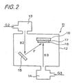
- the second embodiment uses a dual ion beam sputtering method for forming a polymerised passivation film on a ceramic superconductor layer as schematically illustrated in Fig. 2.
- a vacuum chamber 12 of a dual ion beam sputtering apparatus 11 is kept at a vacuum of 1.3 x 10 ⁇ 2 Pa (an exhausting outlet and a vacuum pump are not depicted in Fig. 2).
- An inert gas such as argon is supplied to a plasma generating subchamber 13, as indicated by an arrow G2 in Fig. 2.
- the flow rate of the argon G2 is in the range 5 to 40 standard cubic centimetre per minute (SCCM).
- An argon ion beam B2 generated in the plasma generating subchamber 13 impinges on a target 15 made of fluorocarbon resin such as polytetrafluoroethylene, producing a sputtered beam F of tetrafluoroethylene.
- the energy of the argon ion beam B2 is in the range 20 to 600 eV, so that the sputtered beam F of tetrafluoroethylene from the target 15 is in a molecular state.
- the sputtered beam F impinges on a surface of a ceramic superconductor layer 16, for example a YBaCuO x layer, formed on a SrTiO3 substrate 17 placed on another target 18.
- an inert gas such as argon is supplied to another plasma generating subchamber 14 as indicated by an arrow G3.
- the flow rate of the argon flow G3 is in the range 5 to 40 SCCM.
- An argon ion beam B3 is generated in the plasma generating subchamber 14 and impinges on the surface of the YBaCuO x layer 16.
- the energy of the argon ion beam B3 is in the range 1 to 10 KeV
- the tetrafluoroethylene in the sputtered beam F is assisted by the argon ion beam B3, producing a repolymerised polytetrafluoroethylene film on the surface of the YBaCuO x layer 16 at a growth rate of 1 to 10 nm/min.
- the temperature of the YBaCuO x layer does not exceed 400°C.
- polytetrafluoroethylene is used as the target 15.
- other polyfluorocarbon resins can also be used.
- the materials mentioned above as solid source materials can be used.
- YBaCuO x is used in the above embodiments. However, other materials can be used instead of YBaCuO x .
- the ceramic superconductors can be formed on an Al2O3 or MgO substrate instead of SrTiO3.
- the sputtered beam F from the target 15 is produced by irradiation with the argon ion beam B2 as shown in Fig. 2.
- an electron beam can be used instead of argon ion beam B2.
- the third embodiment relates to an application of a solid source method to a fabrication process for producing an integrated circuit device including ceramic superconductor layers.
- the solid source method is applied to the formation of polymerised passivation films on ceramic superconductor layers in the integrated circuit device.
- the fabricating process, including the processes performed by the solid source method, is illustrated through Figs. 3(a) to 3(i).
- a ceramic superconductor (YBaCuO x ) layer 22 is formed on a substrate (SrTiO3) 21 by a conventional sputtering method.
- substrate Al2O3 or MgO could also be used.
- YBaCuO x superconductor is usually formed on a SrTiO3 substrate, whilst BiSrCaCuO x superconductor is usually formed on a MgO substrate, with a view to eliminating problems due to lattice mismatching.
- the thickness of the YBaCuO x layer 22 is for instance 100 to 200 nm.
- a polytetrafluoroethylene film 23 is formed on the YBaCuO x layer 22 in the same way as described in relation to the first embodiment.
- the thickness of the polytetrafluoroethylene film 23 is controlled so as to be in a range from 0.5 to 100 nm by adjusting deposition rate and deposition time. Normally, the thickness will be set to 10 to 50 nm.
- a resist film 24 about 500 nm thick is coated on the surface of the polytetrafluoroethylene film 23, by a spinner, as shown in Fig. 3(b) and the resist film 14 is exposed through a photomask (not depicted) as indicated by arrows in Fig. 3(c).
- the exposed portion of the resist film is removed by a developer and then water is used for washing, producing a resist pattern 24′ as shown in Fig. 3(d).
- the process of developing the exposed resist is made possible because the polytetrafluoroethylene film 23 protects the ceramic superconductor layer 22 from water and acid such as the developer.
- the polytetrafluoroethylene film 23 is pattern-etched by the conventional argon ion etching technique, using the resist film 24′ as a mask.
- the argon ion etching is performed by using a plasma generating apparatus under conditions such as, for example, pressure of argon 1.3 Pa and RF power in the range 1.3 to 2.6 W/cm2.
- a pattern-etched polytetrafluoroethylene film 23′ fabricated by the argon ion technique described above is shown in Fig. 3(e).
- the YBaCuO x layer 22 is pattern-etched by a conventional reactive ion etching technique, using tetrachloromethane (CCl4).
- the reactive ion etching is performed under conditions such that, for example, the pressure of the CCl4 is 6.5 Pa and RF power is in the range 0.3 to 0.6 W/cm2.
- a pattern-etched YBaCuO x layer 22′ is shown in Fig. 3(f).
- the pattern-etched resist film 24′ and the pattern-etched polytetrafluoroethylene film 23′ are removed by applying oxygen plasma ashing and argon ion etching respectively, leaving the patterned YBaCuO x layer 22′.
- the oxygen plasma ashing is performed under a condition that the pressure of the oxygen is 13 Pa and the RF power is in the range 0.3 to 0.6 W/cm2.
- the patterning of the YBaCuO x layer is accomplished as shown in Fig. 3(g).
- a polytetrafluoroethylene film 25 is formed on the patterned YBaCuO x layer 22′ and partly on the substrate 21, in the same way as described in relation to the first embodiment.
- the thickness of the polytetrafluoroethylene film 25 is in the range 10 to 50 nm.
- the patterned YBaCuO x layer 22′ is protected by the polytetrafluoroethylene film 25 from humidity in the atmosphere, as shown in Fig. 3(h).
- a thick silicon dioxide (SiO2) film 26 is formed on the polytetrafluoroethylene film 25 by a conventional sputtering method.
- a typical thickness of the SiO2 film 26 is 500 nm. This is shown in Fig. 3(i).
- the solid source method is applied; however, a dual ion beam sputtering method, for example as used in the second embodiment, can also be applied.
- a fluorocarbon resin passivation film is formed on a ceramic superconductor by applying either an ion plating method or a dual ion beam sputtering method, using a solid as a source material.
- evaporated tetrafluoroethylene for example, is ionised and accelerated so as to attain an ion beam energy of 1 to 10 KeV by which a polytetrafluoroethylene film is formed on the ceramic superconductor, and in the dual ion beam sputtering method, a sputtered tetrafluoroethylene ion beam, for example, forms a polytetrafluoroethylene film on the ceramic superconductor, assisted by an argon ion beam, for example, having ion energy of 1 to 10 KeV. Either of these methods can be applied in a process for forming a fluorocarbon resin film on a patterned ceramic superconductor layer in a cryoelectronic device.
Landscapes
- Chemical & Material Sciences (AREA)
- Engineering & Computer Science (AREA)
- Chemical Kinetics & Catalysis (AREA)
- Materials Engineering (AREA)
- Mechanical Engineering (AREA)
- Metallurgy (AREA)
- Organic Chemistry (AREA)
- Manufacturing & Machinery (AREA)
- Superconductors And Manufacturing Methods Therefor (AREA)
- Inorganic Compounds Of Heavy Metals (AREA)
- Superconductor Devices And Manufacturing Methods Thereof (AREA)
Applications Claiming Priority (2)
| Application Number | Priority Date | Filing Date | Title |
|---|---|---|---|
| JP110890/88 | 1988-05-07 | ||
| JP63110890A JPH01282175A (ja) | 1988-05-07 | 1988-05-07 | 超伝導材料の保護膜形成方法 |
Publications (2)
| Publication Number | Publication Date |
|---|---|
| EP0341501A2 true EP0341501A2 (de) | 1989-11-15 |
| EP0341501A3 EP0341501A3 (de) | 1990-03-14 |
Family
ID=14547282
Family Applications (1)
| Application Number | Title | Priority Date | Filing Date |
|---|---|---|---|
| EP89107642A Withdrawn EP0341501A3 (de) | 1988-05-07 | 1989-04-27 | Verfahren für die Bildung von Passivierungsschichten auf Supraleitern |
Country Status (2)
| Country | Link |
|---|---|
| EP (1) | EP0341501A3 (de) |
| JP (1) | JPH01282175A (de) |
Cited By (5)
| Publication number | Priority date | Publication date | Assignee | Title |
|---|---|---|---|---|
| WO1991008449A1 (de) * | 1989-12-04 | 1991-06-13 | Institut Für Physik Der Universität Basel Experimentelle Physik Der Kondensierten Materie | Füllstandsdetektor für kryogene flüssigkeiten |
| EP0426000A3 (en) * | 1989-10-30 | 1991-09-04 | Santa Barbara Research Center | Non-aqueous process for delineating patterns on high temperature superconductor films |
| WO1995034096A1 (en) * | 1994-06-03 | 1995-12-14 | E.I. Du Pont De Nemours And Company | Fluoropolymer protectant layer for high temperature superconductor film and photo-definition thereof |
| WO2018052397A1 (en) * | 2016-09-13 | 2018-03-22 | Google Llc | Buffer layer to prevent etching by photoresist developer |
| CN114214597A (zh) * | 2021-12-14 | 2022-03-22 | 国网天津市电力公司电力科学研究院 | 一种超疏水纳米结构有机薄膜的定向生长调控方法 |
Families Citing this family (3)
| Publication number | Priority date | Publication date | Assignee | Title |
|---|---|---|---|---|
| JP2645730B2 (ja) * | 1987-07-27 | 1997-08-25 | 住友電気工業株式会社 | 超電導薄膜 |
| JP4673668B2 (ja) * | 2005-05-17 | 2011-04-20 | 新日本製鐵株式会社 | 酸化物超電導バルク体及びその製造方法 |
| JP5458277B1 (ja) * | 2012-09-27 | 2014-04-02 | ミクロ技研株式会社 | 機能性膜及びその成膜装置、成膜方法 |
-
1988
- 1988-05-07 JP JP63110890A patent/JPH01282175A/ja active Pending
-
1989
- 1989-04-27 EP EP89107642A patent/EP0341501A3/de not_active Withdrawn
Non-Patent Citations (4)
| Title |
|---|
| APPLIED PHYISICS LETTERS, vol. 52, no. 22, 30th May 1988, pages 1897-1898, American Institute of Physics; S. MOROHASHI et al.: "Plasma polymerization for high Tc oxide superconductors" * |
| APPLIED PHYSICS LETTERS, vol. 51, no. 7, 17th August 1987, pages 532-534, American Institute of Physics, New York, US; M.F. YAN et al.: "Water interaction with the superconducting YBa2Cu3O7 phase" * |
| JOURNAL OF VACUUM SCIENCE & TECHNOLOGY A, vol. 3, no. 6, second series, November-December 1985, pages 2627-2628, American Vacuum Society, New York, NY, US; R. D'AGOSTINO: "Summary abstract: mechanisms of polymerization in discharges of fluorocarbons" * |
| JOURNAL OF VACUUM SCIENCE & TECHNOLOTY/SECTION B, vol. 4, no. 6, November/December 1986, pages 1318-1320, American Vacuum Society, Woodbury, NY, US; C.R. FRITZSCHE et al.: "Desposition of polymer film patterns by ion beams" * |
Cited By (6)
| Publication number | Priority date | Publication date | Assignee | Title |
|---|---|---|---|---|
| EP0426000A3 (en) * | 1989-10-30 | 1991-09-04 | Santa Barbara Research Center | Non-aqueous process for delineating patterns on high temperature superconductor films |
| WO1991008449A1 (de) * | 1989-12-04 | 1991-06-13 | Institut Für Physik Der Universität Basel Experimentelle Physik Der Kondensierten Materie | Füllstandsdetektor für kryogene flüssigkeiten |
| WO1995034096A1 (en) * | 1994-06-03 | 1995-12-14 | E.I. Du Pont De Nemours And Company | Fluoropolymer protectant layer for high temperature superconductor film and photo-definition thereof |
| WO2018052397A1 (en) * | 2016-09-13 | 2018-03-22 | Google Llc | Buffer layer to prevent etching by photoresist developer |
| US10811276B2 (en) | 2016-09-13 | 2020-10-20 | Google Llc | Buffer layer to prevent etching by photoresist developer |
| CN114214597A (zh) * | 2021-12-14 | 2022-03-22 | 国网天津市电力公司电力科学研究院 | 一种超疏水纳米结构有机薄膜的定向生长调控方法 |
Also Published As
| Publication number | Publication date |
|---|---|
| EP0341501A3 (de) | 1990-03-14 |
| JPH01282175A (ja) | 1989-11-14 |
Similar Documents
| Publication | Publication Date | Title |
|---|---|---|
| US4912087A (en) | Rapid thermal annealing of superconducting oxide precursor films on Si and SiO2 substrates | |
| US4412902A (en) | Method of fabrication of Josephson tunnel junction | |
| EP0397186B1 (de) | Supraleitende Einrichtung und deren Herstellungsverfahren | |
| Matsui et al. | Reactive ion beam etching of Y‐Ba‐Cu‐O superconductors | |
| EP0337725B1 (de) | Herstellung von supraleitenden Oxidfilmen durch eine pre-Sauerstoff-Stickstoffglühbehandlung | |
| WO1992005591A1 (en) | Improved microelectronic superconducting devices and methods | |
| EP0341501A2 (de) | Verfahren für die Bildung von Passivierungsschichten auf Supraleitern | |
| EP0325765B1 (de) | Josephson-Einrichtung, bestehend aus einer Josephson-Übergangsstruktur, welche für einen Oxidsupraleiter geeignet ist | |
| US5880069A (en) | Process of making high Tc Josephson junction device | |
| US4980338A (en) | Method of producing superconducting ceramic patterns by etching | |
| EP0330211B1 (de) | Polymerisierte organische Passivierungsschicht für Supraleiter | |
| Meng et al. | Very small critical current spreads in Nb/Al-AlOx/Nb integrated circuits using low-temperature and low-stress ECR PECVD silicon oxide films | |
| CA2053549A1 (en) | Construction of high temperature josephson junction device | |
| EP0341502A2 (de) | Kryoelektronische Einrichtung mit einem keramischen Supraleiter | |
| JP2001244511A (ja) | ランプエッジ構造を持つジョセフソン素子の製造方法および成膜装置 | |
| JP2633888B2 (ja) | 超電導デバイス及び超電導配線の製造方法 | |
| Cuculo et al. | Properties of niobium nitride-based Josephson tunnel junctions | |
| JP2822623B2 (ja) | 超伝導体への電極形成方法 | |
| Horibe et al. | Fabrication of natural-barrier ramp-edge Josephson junctions | |
| JP2776004B2 (ja) | ジョセフソン素子の製造方法 | |
| JP2969068B2 (ja) | 超伝導素子の製造方法 | |
| Tsuge et al. | Microfabrication processes for high-T/sub c/superconducting films | |
| Salmi et al. | Thin film process for Nb/NbOx/(Pb-In-Au) Josephson junction devices | |
| CN121586388A (zh) | 一种降低ybco纳米线起翘电压方法 | |
| JP2994190B2 (ja) | 高温超電導薄膜構造およびその作製方法 |
Legal Events
| Date | Code | Title | Description |
|---|---|---|---|
| PUAI | Public reference made under article 153(3) epc to a published international application that has entered the european phase |
Free format text: ORIGINAL CODE: 0009012 |
|
| AK | Designated contracting states |
Kind code of ref document: A2 Designated state(s): DE FR GB |
|
| PUAL | Search report despatched |
Free format text: ORIGINAL CODE: 0009013 |
|
| AK | Designated contracting states |
Kind code of ref document: A3 Designated state(s): DE FR GB |
|
| 16A | New documents despatched to applicant after publication of the search report | ||
| 17P | Request for examination filed |
Effective date: 19900508 |
|
| 17Q | First examination report despatched |
Effective date: 19920430 |
|
| STAA | Information on the status of an ep patent application or granted ep patent |
Free format text: STATUS: THE APPLICATION IS DEEMED TO BE WITHDRAWN |
|
| 18D | Application deemed to be withdrawn |
Effective date: 19921111 |