EP0341122A1 - Matrixförmiger Ladungsübertragungsphotodetektor mit integrierter Ladungsfiltervorrichtung - Google Patents
Matrixförmiger Ladungsübertragungsphotodetektor mit integrierter Ladungsfiltervorrichtung Download PDFInfo
- Publication number
- EP0341122A1 EP0341122A1 EP89401129A EP89401129A EP0341122A1 EP 0341122 A1 EP0341122 A1 EP 0341122A1 EP 89401129 A EP89401129 A EP 89401129A EP 89401129 A EP89401129 A EP 89401129A EP 0341122 A1 EP0341122 A1 EP 0341122A1
- Authority
- EP
- European Patent Office
- Prior art keywords
- zone
- transfer
- auxiliary
- low
- type
- Prior art date
- Legal status (The legal status is an assumption and is not a legal conclusion. Google has not performed a legal analysis and makes no representation as to the accuracy of the status listed.)
- Withdrawn
Links
- 239000011159 matrix material Substances 0.000 title claims abstract description 20
- 238000001914 filtration Methods 0.000 title claims abstract description 17
- 239000000758 substrate Substances 0.000 claims abstract description 23
- 101150101414 PRP1 gene Proteins 0.000 claims abstract description 3
- 101100368710 Rattus norvegicus Tacstd2 gene Proteins 0.000 claims abstract description 3
- 101100342406 Saccharomyces cerevisiae (strain ATCC 204508 / S288c) PRS1 gene Proteins 0.000 claims abstract description 3
- 230000005855 radiation Effects 0.000 claims description 6
- 239000004065 semiconductor Substances 0.000 claims description 3
- 101000951145 Homo sapiens Succinate dehydrogenase [ubiquinone] cytochrome b small subunit, mitochondrial Proteins 0.000 claims 1
- 102100038014 Succinate dehydrogenase [ubiquinone] cytochrome b small subunit, mitochondrial Human genes 0.000 claims 1
- 230000007704 transition Effects 0.000 abstract description 4
- 239000012535 impurity Substances 0.000 description 9
- 238000010586 diagram Methods 0.000 description 6
- 230000009471 action Effects 0.000 description 5
- 239000000470 constituent Substances 0.000 description 5
- 230000006870 function Effects 0.000 description 5
- 238000009792 diffusion process Methods 0.000 description 4
- 238000000034 method Methods 0.000 description 4
- 230000010354 integration Effects 0.000 description 3
- VYPSYNLAJGMNEJ-UHFFFAOYSA-N Silicium dioxide Chemical compound O=[Si]=O VYPSYNLAJGMNEJ-UHFFFAOYSA-N 0.000 description 2
- XUIMIQQOPSSXEZ-UHFFFAOYSA-N Silicon Chemical compound [Si] XUIMIQQOPSSXEZ-UHFFFAOYSA-N 0.000 description 2
- 230000008859 change Effects 0.000 description 2
- 238000002513 implantation Methods 0.000 description 2
- 229910052710 silicon Inorganic materials 0.000 description 2
- 239000010703 silicon Substances 0.000 description 2
- 229910052814 silicon oxide Inorganic materials 0.000 description 2
- 241001644893 Entandrophragma utile Species 0.000 description 1
- 238000009825 accumulation Methods 0.000 description 1
- 239000003990 capacitor Substances 0.000 description 1
- 230000008878 coupling Effects 0.000 description 1
- 238000010168 coupling process Methods 0.000 description 1
- 238000005859 coupling reaction Methods 0.000 description 1
- 238000005286 illumination Methods 0.000 description 1
- 238000004519 manufacturing process Methods 0.000 description 1
- 238000005036 potential barrier Methods 0.000 description 1
- 230000008569 process Effects 0.000 description 1
- 230000009467 reduction Effects 0.000 description 1
Images


Classifications
-
- H—ELECTRICITY
- H10—SEMICONDUCTOR DEVICES; ELECTRIC SOLID-STATE DEVICES NOT OTHERWISE PROVIDED FOR
- H10F—INORGANIC SEMICONDUCTOR DEVICES SENSITIVE TO INFRARED RADIATION, LIGHT, ELECTROMAGNETIC RADIATION OF SHORTER WAVELENGTH OR CORPUSCULAR RADIATION
- H10F39/00—Integrated devices, or assemblies of multiple devices, comprising at least one element covered by group H10F30/00, e.g. radiation detectors comprising photodiode arrays
- H10F39/10—Integrated devices
- H10F39/12—Image sensors
- H10F39/15—Charge-coupled device [CCD] image sensors
- H10F39/153—Two-dimensional or three-dimensional array CCD image sensors
-
- H—ELECTRICITY
- H04—ELECTRIC COMMUNICATION TECHNIQUE
- H04N—PICTORIAL COMMUNICATION, e.g. TELEVISION
- H04N25/00—Circuitry of solid-state image sensors [SSIS]; Control thereof
- H04N25/40—Extracting pixel data from image sensors by controlling scanning circuits, e.g. by modifying the number of pixels sampled or to be sampled
- H04N25/44—Extracting pixel data from image sensors by controlling scanning circuits, e.g. by modifying the number of pixels sampled or to be sampled by partially reading an SSIS array
- H04N25/443—Extracting pixel data from image sensors by controlling scanning circuits, e.g. by modifying the number of pixels sampled or to be sampled by partially reading an SSIS array by reading pixels from selected 2D regions of the array, e.g. for windowing or digital zooming
-
- H—ELECTRICITY
- H04—ELECTRIC COMMUNICATION TECHNIQUE
- H04N—PICTORIAL COMMUNICATION, e.g. TELEVISION
- H04N25/00—Circuitry of solid-state image sensors [SSIS]; Control thereof
- H04N25/60—Noise processing, e.g. detecting, correcting, reducing or removing noise
- H04N25/62—Detection or reduction of noise due to excess charges produced by the exposure, e.g. smear, blooming, ghost image, crosstalk or leakage between pixels
- H04N25/621—Detection or reduction of noise due to excess charges produced by the exposure, e.g. smear, blooming, ghost image, crosstalk or leakage between pixels for the control of blooming
-
- H—ELECTRICITY
- H04—ELECTRIC COMMUNICATION TECHNIQUE
- H04N—PICTORIAL COMMUNICATION, e.g. TELEVISION
- H04N25/00—Circuitry of solid-state image sensors [SSIS]; Control thereof
- H04N25/70—SSIS architectures; Circuits associated therewith
- H04N25/71—Charge-coupled device [CCD] sensors; Charge-transfer registers specially adapted for CCD sensors
- H04N25/72—Charge-coupled device [CCD] sensors; Charge-transfer registers specially adapted for CCD sensors using frame transfer [FT]
Definitions
- the invention relates to matrix photodetectors with charge transfer of the type comprising filtering means for outputting only payloads corresponding to a useful portion of incident light radiation.
- Photodetectors are used in principle to store, transfer and deliver loads as a function of the incident light radiation to which they are subjected, in order to restore a digital image.
- the photodetectors a distinction is made between those which generally have a single row (or strip) of photosensitive elements and those, surface or matrix, organized either in frame transfer or in interline transfer and which are constituted by sets of channels of parallel load transfer.
- the invention relates only to matrix photodetectors.
- FIG. 1 schematically represents a conventional matrix photodetector organized in frame transfer.
- This photodetector 1 comprises a first zone 1 comprising a photosensitive sub-zone 10, commonly called the image zone and a non-photosensitive sub-zone 11, commonly called the memory zone.
- the photodetector 1 also includes a second zone 2 connected to the first zone 1 comprising a read register 20, extended by a read diode 21 connected to a control transistor 22.
- the image area 10 is a matrix comprising n rows and p columns. Each column is a vertical charge transfer shift register constituting a charge transfer channel.
- the register boxes are photo sensitive and charges accumulate there depending on the illumination of the hut.
- the memory zone is constituted in an identical manner to the image zone but but the boxes of the various registers are not photosensitive.
- the read register is a horizontal shift register.
- the image and memory areas also include transfer grids surmounting the transfer channels and suitable for receiving low or high control signals to apply a low or high potential level to the transfer channels so as to allow charge transfer there.
- the read register is suitable for receiving at least part of the charges stored in the memory area and is surmounted by a read grid suitable for also receiving low or high control signals to apply a low potential level to the read register. or high, so as to allow the transfer of the charges contained in this read register into the read diode.
- FIG. 2 schematically illustrates a matrix photodetector organized in interline transfer.
- the image area 10 ′ is constituted by columns of photodiodes interconnected with columns of photosensitive cells belonging to vertical shift registers constituting the memory area 11 ′.
- the lower part of each transfer channel CT ′ is connected to a box of a horizontal shift register constituting the read register 20 ′.
- the operating principle of a photodetector organized in interline transfer is substantially similar.
- the charges stored in the photodiodes are transferred horizontally to the shift registers then each line of the shift registers is shifted vertically in the reading register and transferred to the reading medium by a horizontal shift of the latter.
- FIGS. 3A to 3C schematically illustrate a filtering principle currently used in the state of the art for outputting only payloads corresponding to said useful portion IMD of the incident light radiation IM, that is to say to the portion of the image you want to view.
- Figure 3A shows the desired image IMD.
- the total image IM including the desired image IMD, is shown already transferred in the memory area 11.
- SCM control signal
- control signal SCL under the action of the control signal SCL, low or high, applied to the reading grid, transfers the line it contains into the reading diode.
- This line is then, effectively or not, output at the control of the filtering control signal SCF which is, in fact, a control clock of the gate of the control transistor.
- SCF filtering control signal
- the control signal SCF exhibits a change of state (up / down or the reverse) during the action of control signal SCL
- the line present in the read register is effectively transferred into the read diode then output, while, when the SCF control signal is high, the read diode is reset to 0 and no line is delivered.
- the control transistor 22 and the control signal SCF therefore form part of the filtering means.
- FIG. 3C A timing diagram of the image restitution, present in the memory area, is illustrated in FIG. 3C.
- the reading register is assumed to have only one line.
- the first i pulses of the control signal SCM the first i lines of the image IM are successively transferred to the read register 2. This, under the action of the first i pulses of the control signal SCL, releases these lines.
- the control signal SCF being meanwhile constantly high, none of these lines is actually delivered at the output of the photodetector. We therefore eliminated unnecessary charges corresponding to lines 1 to i of the image.
- the present invention overcomes these drawbacks by proposing a matrix photodetector provided with means for filtering the payloads which do not require oversizing of the reading register and allowing a very high image scanning rate.
- the subject of the invention is therefore a matrix photodetector charge transfer of the type comprising: a first zone, partly photosensitive, in which said charges are stored and comprising, on a semiconductor substrate: . a plurality of parallel charge transfer channels, . transfer grids surmounting the transfer channels and suitable for receiving low or high control signals to apply a low or high potential level to the transfer channels, so as to allow charge transfer there, a second zone, connected to the first zone, capable of receiving at least a portion of the charges stored in the first zone, and comprising . a read register extended by a read diode, .
- a reading grid surmounting the reading register and suitable for receiving low or high control signals to apply a low or high potential level to the reading register, so as to allow the transfer of the charges contained in the reading register into the reading diode, and, .
- filtering means acting on the reading diode so as to deliver only payloads at the output corresponding to a useful portion of the incident light radiation, characterized in that the filtering means comprise, in the first zone, an auxiliary zone comprising an implanted region of a type opposite to that of the substrate, parallel to the transfer channels and followed by a region passage of charges, located in the extension of the transfer channels, and surmounted by an auxiliary grid suitable for receiving low or high control auxiliary signals, to apply to the passage region low or high auxiliary potential levels, respectively in absolute value below the low or high potential levels produced by the other grids, which allows a first filtering of the charges before their transfer to the reading register.
- the auxiliary zone comprises an anti-dazzle device of the type with an insulating zone, that is to say of the type described in French Patent Application No. 82-11395, in the name of the Applicant.
- the passage region comprises an implanted portion of type identical to that of the substrate and the low or high control signals are then respectively identical in amplitude to the low or high control signals of the other grids.
- the low or high auxiliary control signals have different amplitudes from the respective ones of the other low or high control signals.
- the photodetector is of the frame transfer type and the auxiliary zone is located at the bottom of the image zone.
- the photodetector is of the frame transfer type and the auxiliary area is located at the end of the memory area.
- the photodetector can also be of the interline transfer type and the auxiliary zone is then located at the bottom of the memory zone.
- the photodetector according to the invention can be equipped with at least one other anti-dazzle device of the type with an insulating zone situated in the photosensitive part of the first zone.
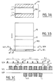
- FIG. 4 schematically represents a first embodiment of the photodetector according to the invention.
- the photodetector is of the raster transfer matrix type and it can be seen that the image area 10 comprises n + 1 lines, one line more than in a conventional photodetector of the prior art.
- the nth line of the image zone that is to say the penultimate line, comprises implanted regions of type opposite to that of the substrate, parallel to the transfer channels. These implanted regions, as well as the additional line n + 1, form part of an auxiliary zone 100 which will be detailed below, and which is therefore located at the bottom of the image zone.
- FIG. 5 schematically represents a second embodiment of the frame transfer matrix photodetector.
- the memory area 11 comprises n ⁇ 1 lines, that is to say one line more than in a prior art photodetector.
- the auxiliary area 110 is analogous to the auxiliary area 100 and is located on the lines n and n + 1 of the memory area 11, respectively referenced 11d and 11g, that is to say at the bottom of the memory area.
- FIG. 6 schematically represents a third embodiment of a photodetector according to the invention in the case where it is of the interline transfer type.
- the transfer channels CT ′ of the memory area 11 ′ comprise n + 1 boxes, and an auxiliary area 110 ′ similar to the auxiliary areas 100 and 110 is defined, located at the bottom of the memory area.
- FIGS. 7 to 10 describe, in detail, the structure of an auxiliary zone 110, located at the bottom of the memory zone 11, in the case of a matrix photodetector with frame transfer.
- FIGS. 7 to 10 therefore show more precisely the lines n-1, n and n + 1 of the memory area 11, respectively referenced 11a, 11d and 11g.
- the charge transfer photodetector comprises a semiconductor substrate S such as P-type silicon, for example, covered at least in part with an insulating layer 40, made for example of silicon oxide.
- a transfer channel CT has been shown in which the charges are capable of being transferred longitudinally in the direction of the arrow F.
- Each of the lines of the matrix photodetector comprises transfer grids such as GTa and GTd, covering the transfer channel CT and arranged substantially perpendicular to the direction of the charge transfer.
- the assembly (grid - insulating layer - substrate) defines in the CT transfer channel capacitors of the type with charge coupling.
- the transfer channel portion located on line 11d, includes an anti-dazzle device of the type described in French Patent Application No. 82-11395.
- This anti-glare device will be designated subsequently under the name "anti-glare device of the type with insulating zone”.
- the main constituent elements as well as the main operating principles will be recalled below, those skilled in the art can refer to the above-mentioned French Patent Application No. 82-11395 for more details.
- the CT transfer channel comprises, in the case where the charge is transferred in volume, an implantation of impurities 50 of a type opposite to that of the substrate which occupies the entire width of this CT channel.
- the insulating zone type anti-dazzle device is located between two adjacent transfer channels. This device comprises a diode D formed by an implanted region of the type opposite to that of the substrate, that is to say of the N type and parallel to the transfer channel CT. This device also includes a transition zone ZT ensuring a reduction in the surface potential of the substrate, the surface potential of this transition zone ZT varying as a function of the potential applied to the grid GTd.
- the diode D and the transfer zone ZT are surrounded on all sides, with the exception of that contiguous to the transfer channel CT, by an insulating zone ZI, such as the surface potential in the substrate, under this insulating zone, ie null and invariable as a function of the voltages applied to the GTd grids as well as to the adjacent grids.
- this insulating zone ZI can be produced by implanting impurities of the same type as that of the substrate with a higher concentration of impurities. at 1019 atoms / cm3, or by an insulating deposit such as silicon oxide under a thickness of approximately 1 micron.
- This insulating zone ZI extends on line 11a to be contiguous to the portion of transfer channel CT covered with the grid GTa.
- the additional line 11g comprises a portion of transfer channel having between the diffusion of impurities 50 and the insulating zone 40 a diffusion of impurities 60 of the type opposite to the diffusion of impurities 50, therefore of the same type as that of the substrate, that is to say of the P type.
- This transfer channel portion constitutes a passage region RP for the charges passing from the memory area 11 to the read register 20.
- This transfer region RP therefore extends the channel CT in the memory area 11.
- Line 11g also includes the extension of the insulating area ZI parallel to the passage region RP.
- the auxiliary zone 110 includes the anti-dazzle device of the insulating zone type comprising the diode D, the transition zone ZT and the insulating zone ZI, as well as the passage region RP covered with an auxiliary grid GA of the same type as the transfer grids GTa and GTd.
- This auxiliary grid GA is controlled independently of the other transfer grids and of the reading grid GL.
- FIGS. 8A to 10A illustrate, schematically, the evolution of the surface potentials PS of the different regions of the substrate.
- each grid is controlled by a low or high control signal which gives the area located under the grid a low or high potential level.
- the reference of the potential level of an area will be assigned the suffix 0 for a low potential level and the suffix 1 for a high potential level. So the low potential level of the serving transfer channel, located under the GTa transfer grid, will be assigned the reference PGa0.
- FIGS. 8A, 9A and 10A show that the surface potential PZI, in the insulating zone ZI, is zero and invariable as a function of the potentials applied to the different grids.
- the first part of FIG. 9A shows the evolution of the surface potential PS when the transfer gate GTd is activated by the low control signal and the second part of this same figure 9A shows the evolution of the surface potentials when the gate transfer signal GTd is activated by the control signal O. In the latter case, when there is charge accumulation and exceeding the anti-glare level NAE, there is evacuation of excess charges towards the potential well formed by the diode D.
- the level of the high potential PZT1, of the transfer zone must be higher than the level of low potential PGd0, so that the charges in excess go preferably towards the diode D instead of overflowing in the direction of transfer to other potential wells.
- FIG. 10A illustrates the evolution of the surface potential under the auxiliary grid GA, the latter being subjected to a low or high auxiliary control signal.
- the auxiliary control signals of the auxiliary grid GA are identical in amplitude to the control signals of the transfer and reading grids, but the compensation caused by the diffusion of the impurity zone 60 causes a PRP potential level in the RP passage area different from the potential levels in the rest of the transfer channel.
- the surface potential PRP0 of the passage region is lower than the potential PGd0 and when the auxiliary gate is activated by the auxiliary control signal in the high state, the high potential level PRP1 of the passage region is lower than the potential levels PGd1 but higher than the anti-dazzle level NAE.
- FIG. 11 schematically illustrates a longitudinal section of the lines 11a, 11d and 11g as well as of the reading register 20, this section showing the implantation of impurities 60 of the same type as the substrate.
- FIG. 11A shows the evolution of the surface potential corresponding to the section of FIG. 11, in a particular case of operation. It is assumed, in this case, that the transfer gate GTa is activated by the control signal in the low state, that the transfer gate GTd is activated by the control signal in the high state, as well as for the reading grid GL, while the auxiliary grid is activated by the auxiliary control signal in the low state.
- FIG. 11A therefore shows the positioning of the different potential levels with respect to each other.
- the auxiliary control signals of the auxiliary grid GA can be different in amplitude with respect to the control signals of the other grids, so as to apply to the auxiliary grid a voltage lower than that of the other grids to respect the scale of potential levels.
- FIGS. 11A and 12 will now serve to illustrate the operating principle of the photodetector according to the invention.
- the reference SCM designates the control signal applied to the different transfer grids of the memory area
- the reference SCL designates the control signal applied to the reading grid GL
- the reference SCA designates the auxiliary control signal applied to the auxiliary gate
- the reference SCF designates the filtering control signal applied to the control transistor 22.
- the auxiliary control signal SCA is low applying to the passage region RP a low potential level PRP0.
- the charges corresponding to lines 1 to i-1 then "accumulate" against the potential barrier formed under the grid GA and when the level of these charges exceeds the anti-glare level NAE, the excess charges, therefore unnecessary charges , are eliminated by the anti-glare device of the type with insulating zone.
- the control signal SCA is high as well as the control signal of the reading gate SCL.
- pulses i + 1 to j This is also true for the pulses i + 1 to j.
- the unnecessary charges corresponding to line i are then transferred to the read register and then to the read diode and are eliminated using the high control signal SCF.
- the other charges corresponding to the lines i + 1 to j, therefore the payloads, are effectively delivered at the output to restore the desired image IMP.
- An arrangement identical to that used for pulses 1 to i is used for pulses j + 1 to n, the pulses j + 1 to n-1 being discharged by the anti-dazzle device of the type with insulating zone while the pulse n is evacuated using the SCF filtering control signal.
- the anti-dazzle device of the insulating zone type and of the additional line 11g provided with the auxiliary grid GA which allows a first filtering of the payloads before their transfer into the reading register.
- the latter does not need to be oversized since it only evacuates a single unnecessary line.
- the number of unnecessary line summations is unlimited and the lower the number of lines, the shorter the recurrence time between two images.
- auxiliary zone 110 ′ placed at the bottom of the memory zone in the case of a matrix photodetector with interline transfer would operate in an identical manner.
- auxiliary zone comprises, in addition to the passage region surmounted by the auxiliary grid, an implanted region of the type opposite to that of the substrate, as used for example in the anti-glare devices of the prior art described in French Patent Application 82-11395.
- the invention may include variants, in particular the following: -
- the invention has been described using a P-type silicon substrate but it is obvious to those skilled in the art that it is not limited to this type of substrate or to the type of impurities used. However, in the case of an N-type substrate, the signs of the charges and of the potentials will be reversed with respect to the P-type substrate described above, the transfer zone ZT then ensuring an increase in the surface potential while the auxiliary potential levels, low or high, of the passage region will be respectively lower in absolute value than the potential levels, low or high, produced by the other grids; -
- a photodetector according to the invention may include in the image area at least one other anti-dazzle device of the type with an insulating area, this other device then ensuring its own function as described in French Patent Application No. 82-11395.
Landscapes
- Engineering & Computer Science (AREA)
- Multimedia (AREA)
- Signal Processing (AREA)
- Solid State Image Pick-Up Elements (AREA)
- Transforming Light Signals Into Electric Signals (AREA)
Applications Claiming Priority (2)
| Application Number | Priority Date | Filing Date | Title |
|---|---|---|---|
| FR8805904A FR2631188A1 (fr) | 1988-05-03 | 1988-05-03 | Photodetecteur matriciel a transfert de charges avec dispositif integre de filtrage de charges |
| FR8805904 | 1988-05-03 |
Publications (1)
| Publication Number | Publication Date |
|---|---|
| EP0341122A1 true EP0341122A1 (de) | 1989-11-08 |
Family
ID=9365926
Family Applications (1)
| Application Number | Title | Priority Date | Filing Date |
|---|---|---|---|
| EP89401129A Withdrawn EP0341122A1 (de) | 1988-05-03 | 1989-04-21 | Matrixförmiger Ladungsübertragungsphotodetektor mit integrierter Ladungsfiltervorrichtung |
Country Status (4)
| Country | Link |
|---|---|
| US (1) | US4881249A (de) |
| EP (1) | EP0341122A1 (de) |
| JP (1) | JPH0216769A (de) |
| FR (1) | FR2631188A1 (de) |
Cited By (14)
| Publication number | Priority date | Publication date | Assignee | Title |
|---|---|---|---|---|
| EP0421243A3 (en) * | 1989-09-29 | 1993-05-12 | Sanyo Electric Co., Ltd. | Automatic focusing camera |
| WO2000025511A1 (en) * | 1998-10-23 | 2000-05-04 | Cognex Corporation | Methods and apparatus for charge coupled device image acquisition with selective vertical readout |
| US6608647B1 (en) | 1997-06-24 | 2003-08-19 | Cognex Corporation | Methods and apparatus for charge coupled device image acquisition with independent integration and readout |
| US6687402B1 (en) | 1998-12-18 | 2004-02-03 | Cognex Corporation | Machine vision methods and systems for boundary feature comparison of patterns and images |
| US7006669B1 (en) | 2000-12-31 | 2006-02-28 | Cognex Corporation | Machine vision method and apparatus for thresholding images of non-uniform materials |
| US7639861B2 (en) | 2005-09-14 | 2009-12-29 | Cognex Technology And Investment Corporation | Method and apparatus for backlighting a wafer during alignment |
| US8111904B2 (en) | 2005-10-07 | 2012-02-07 | Cognex Technology And Investment Corp. | Methods and apparatus for practical 3D vision system |
| US8126260B2 (en) | 2007-05-29 | 2012-02-28 | Cognex Corporation | System and method for locating a three-dimensional object using machine vision |
| US8162584B2 (en) | 2006-08-23 | 2012-04-24 | Cognex Corporation | Method and apparatus for semiconductor wafer alignment |
| US8867847B2 (en) | 1998-07-13 | 2014-10-21 | Cognex Technology And Investment Corporation | Method for fast, robust, multi-dimensional pattern recognition |
| US9124873B2 (en) | 2010-12-08 | 2015-09-01 | Cognex Corporation | System and method for finding correspondence between cameras in a three-dimensional vision system |
| US9147252B2 (en) | 2003-07-22 | 2015-09-29 | Cognex Technology And Investment Llc | Method for partitioning a pattern into optimized sub-patterns |
| US9393694B2 (en) | 2010-05-14 | 2016-07-19 | Cognex Corporation | System and method for robust calibration between a machine vision system and a robot |
| US9734419B1 (en) | 2008-12-30 | 2017-08-15 | Cognex Corporation | System and method for validating camera calibration in a vision system |
Families Citing this family (4)
| Publication number | Priority date | Publication date | Assignee | Title |
|---|---|---|---|---|
| US4974043A (en) * | 1989-10-12 | 1990-11-27 | Eastman Kodak Company | Solid-state image sensor |
| DE69632172T2 (de) * | 1995-02-21 | 2005-04-21 | Dalsa Corp | Ladungsgekoppelte bildaufnahmeanordnung |
| US9533418B2 (en) | 2009-05-29 | 2017-01-03 | Cognex Corporation | Methods and apparatus for practical 3D vision system |
| US9679224B2 (en) | 2013-06-28 | 2017-06-13 | Cognex Corporation | Semi-supervised method for training multiple pattern recognition and registration tool models |
Citations (4)
| Publication number | Priority date | Publication date | Assignee | Title |
|---|---|---|---|---|
| EP0083376A1 (de) * | 1981-07-13 | 1983-07-13 | Sony Corporation | Festkörper-bildaufnahmeeinrichtung |
| FR2548497A1 (fr) * | 1983-06-28 | 1985-01-04 | Thomson Csf | Capteur d'image a transfert de trame de format variable |
| EP0163547A2 (de) * | 1984-05-31 | 1985-12-04 | Fujitsu Limited | Bildwandler |
| EP0235002A1 (de) * | 1986-02-07 | 1987-09-02 | AEROSPATIALE Société Nationale Industrielle | Optoelektronischer Ladungübertragungssensor |
Family Cites Families (2)
| Publication number | Priority date | Publication date | Assignee | Title |
|---|---|---|---|---|
| JPS5827712B2 (ja) * | 1975-12-25 | 1983-06-10 | 株式会社東芝 | コタイサツゾウソウチ |
| JPH0815319B2 (ja) * | 1984-04-13 | 1996-02-14 | 株式会社東芝 | 固体撮像装置の駆動方法 |
-
1988
- 1988-05-03 FR FR8805904A patent/FR2631188A1/fr not_active Withdrawn
-
1989
- 1989-04-21 EP EP89401129A patent/EP0341122A1/de not_active Withdrawn
- 1989-05-01 US US07/345,232 patent/US4881249A/en not_active Expired - Fee Related
- 1989-05-01 JP JP1112807A patent/JPH0216769A/ja active Pending
Patent Citations (4)
| Publication number | Priority date | Publication date | Assignee | Title |
|---|---|---|---|---|
| EP0083376A1 (de) * | 1981-07-13 | 1983-07-13 | Sony Corporation | Festkörper-bildaufnahmeeinrichtung |
| FR2548497A1 (fr) * | 1983-06-28 | 1985-01-04 | Thomson Csf | Capteur d'image a transfert de trame de format variable |
| EP0163547A2 (de) * | 1984-05-31 | 1985-12-04 | Fujitsu Limited | Bildwandler |
| EP0235002A1 (de) * | 1986-02-07 | 1987-09-02 | AEROSPATIALE Société Nationale Industrielle | Optoelektronischer Ladungübertragungssensor |
Non-Patent Citations (2)
| Title |
|---|
| IEEE 1987-SOLID STATE CIRCUITS CONFERENCE, vol. 30, 1ère édition, février 1987, pages 106-107, IEEE, New York, US; T. YAMADA et al.: "A line-address CCD image sensor" * |
| PATENT ABSTRACTS OF JAPAN, vol. 10, no. 65 (E-388)[2122], 14 mars 1986; & JP-A-60 217 661 (TOSHIBA K.K.) 31-10-1985 * |
Cited By (14)
| Publication number | Priority date | Publication date | Assignee | Title |
|---|---|---|---|---|
| EP0421243A3 (en) * | 1989-09-29 | 1993-05-12 | Sanyo Electric Co., Ltd. | Automatic focusing camera |
| US6608647B1 (en) | 1997-06-24 | 2003-08-19 | Cognex Corporation | Methods and apparatus for charge coupled device image acquisition with independent integration and readout |
| US8867847B2 (en) | 1998-07-13 | 2014-10-21 | Cognex Technology And Investment Corporation | Method for fast, robust, multi-dimensional pattern recognition |
| WO2000025511A1 (en) * | 1998-10-23 | 2000-05-04 | Cognex Corporation | Methods and apparatus for charge coupled device image acquisition with selective vertical readout |
| US6687402B1 (en) | 1998-12-18 | 2004-02-03 | Cognex Corporation | Machine vision methods and systems for boundary feature comparison of patterns and images |
| US7006669B1 (en) | 2000-12-31 | 2006-02-28 | Cognex Corporation | Machine vision method and apparatus for thresholding images of non-uniform materials |
| US9147252B2 (en) | 2003-07-22 | 2015-09-29 | Cognex Technology And Investment Llc | Method for partitioning a pattern into optimized sub-patterns |
| US7639861B2 (en) | 2005-09-14 | 2009-12-29 | Cognex Technology And Investment Corporation | Method and apparatus for backlighting a wafer during alignment |
| US8111904B2 (en) | 2005-10-07 | 2012-02-07 | Cognex Technology And Investment Corp. | Methods and apparatus for practical 3D vision system |
| US8162584B2 (en) | 2006-08-23 | 2012-04-24 | Cognex Corporation | Method and apparatus for semiconductor wafer alignment |
| US8126260B2 (en) | 2007-05-29 | 2012-02-28 | Cognex Corporation | System and method for locating a three-dimensional object using machine vision |
| US9734419B1 (en) | 2008-12-30 | 2017-08-15 | Cognex Corporation | System and method for validating camera calibration in a vision system |
| US9393694B2 (en) | 2010-05-14 | 2016-07-19 | Cognex Corporation | System and method for robust calibration between a machine vision system and a robot |
| US9124873B2 (en) | 2010-12-08 | 2015-09-01 | Cognex Corporation | System and method for finding correspondence between cameras in a three-dimensional vision system |
Also Published As
| Publication number | Publication date |
|---|---|
| FR2631188A1 (fr) | 1989-11-10 |
| JPH0216769A (ja) | 1990-01-19 |
| US4881249A (en) | 1989-11-14 |
Similar Documents
| Publication | Publication Date | Title |
|---|---|---|
| EP0341122A1 (de) | Matrixförmiger Ladungsübertragungsphotodetektor mit integrierter Ladungsfiltervorrichtung | |
| EP3188238B1 (de) | Flugzeit-erfassungspixel | |
| EP0145543B1 (de) | Ladungsgekoppelte mehrzeilige lineare Anordnung | |
| EP0064890B1 (de) | Einen Zeilenspeicher umfassende Einrichtung zur Bildabtastung in aufeinanderfolgenden Zeilen unter Verwendung elektrischer Ladungsübertragung und Fernsehkamera mit einer solchen Einrichtung | |
| EP0474550B1 (de) | Bilddetektor mit Grossformat-Pixels | |
| EP0038725A1 (de) | Photoempfindliche Vorrichtung, die durch Ladungsübertragung abgelesen wird, sowie eine Fernsehkamera, die eine solche Vorrichtung enthält | |
| EP0435773B1 (de) | Bildaufnahmeeinrichtung mit integrierten Ablenkschaltungen | |
| EP0114768B1 (de) | Lichtempfindliche Ladungstransfervorrichtung | |
| EP3405977B1 (de) | Mehrreihiger bildsensor mit ladungsübertragung mit integrationszeitanpassung | |
| EP3308399B1 (de) | Bildsensor mit hohem dynamikbereich und dreiteiligem speicherknoten | |
| EP1627432B1 (de) | Cmos bildaufnahmevorrichtung | |
| EP0276594B1 (de) | Überlaufvorrichtung für einen Ladungsübertragungs-Bildsensor und eine solche Vorrichtung enthaltender Bildsensor | |
| EP0068975B1 (de) | Festkörperlichtdetektor mit Ladungsübertragungsleser und Bildaufnahmeeinrichtung mit einem solchen Detektor | |
| EP0390644B1 (de) | CCD-Ausleseschaltung mit einer grossen Ausgangsdynamik | |
| EP0424241B1 (de) | Bilddetektor mit grosser Speicherkapazität pro Pixel | |
| WO2015055501A1 (fr) | Capteur d'image a multiplication d'electrons et a lecture regroupee de pixels | |
| FR2571572A1 (fr) | Dispositif photosensible a transfert de ligne muni d'amplificateurs de contre-reaction | |
| FR2565753A1 (fr) | Procede de commande de la sensibilite d'un dispositif photosensible a transfert de charges, et dispositif pour la mise en oeuvre de ce procede | |
| EP1606934B1 (de) | Bildsensor mit schnellem lesezyklus | |
| FR3131440A1 (fr) | Capteur d'images et procédé de fabrication d'un tel capteur | |
| FR2667210A1 (fr) | Capteur d'image ccd a temps de chargement reduit. | |
| FR2794896A1 (fr) | Dispositif photosensible du type utilisant une zone memoire | |
| FR2672759A1 (fr) | Capteur d'images a semiconducteurs, a stockage de charge. | |
| FR2588140A1 (fr) | Dispositif de detection avec accumulation en phase des signaux. |
Legal Events
| Date | Code | Title | Description |
|---|---|---|---|
| PUAI | Public reference made under article 153(3) epc to a published international application that has entered the european phase |
Free format text: ORIGINAL CODE: 0009012 |
|
| AK | Designated contracting states |
Kind code of ref document: A1 Designated state(s): DE FR GB NL |
|
| 17P | Request for examination filed |
Effective date: 19891202 |
|
| 17Q | First examination report despatched |
Effective date: 19920520 |
|
| STAA | Information on the status of an ep patent application or granted ep patent |
Free format text: STATUS: THE APPLICATION IS DEEMED TO BE WITHDRAWN |
|
| 18D | Application deemed to be withdrawn |
Effective date: 19921001 |