EP0340439A2 - Switched capacitor amplifier circuit - Google Patents
Switched capacitor amplifier circuit Download PDFInfo
- Publication number
- EP0340439A2 EP0340439A2 EP89105134A EP89105134A EP0340439A2 EP 0340439 A2 EP0340439 A2 EP 0340439A2 EP 89105134 A EP89105134 A EP 89105134A EP 89105134 A EP89105134 A EP 89105134A EP 0340439 A2 EP0340439 A2 EP 0340439A2
- Authority
- EP
- European Patent Office
- Prior art keywords
- input
- capacitor
- plate
- output
- feedback
- Prior art date
- Legal status (The legal status is an assumption and is not a legal conclusion. Google has not performed a legal analysis and makes no representation as to the accuracy of the status listed.)
- Granted
Links
Images


Classifications
-
- H—ELECTRICITY
- H03—ELECTRONIC CIRCUITRY
- H03F—AMPLIFIERS
- H03F3/00—Amplifiers with only discharge tubes or only semiconductor devices as amplifying elements
- H03F3/005—Amplifiers with only discharge tubes or only semiconductor devices as amplifying elements using switched capacitors, e.g. dynamic amplifiers; using switched capacitors as resistors in differential amplifiers
Definitions
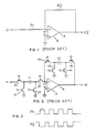
- FIG. 1 An amplifier circuit known in the art is shown in Figure 1.
- This circuit uses an operational amplifier 12 with an inverting input terminal 14, a non-inverting input terminal 16, and a single output terminal 18.
- the input signal V1 passes through the input resistor R1 to the inverting input terminal 14.
- the non-inverting input terminal is connected to ground.
- the output signal at the output terminal 18 provides the amplifier circuit output signal at output node V2.
- the output signal is also returned through feedback resistor R2 to the inverting input terminal 14.
- the gain and other response characteristics from the V1 node to the V2 node of this circuit are determined by the elements in the feedback path from the output terminal 18 back to the inverting input terminal 14.
- the voltage gain, V2 / V1 of the circuit is set by the ratio of the feedback resistor R2 to the input resistor R1. Capacitors are sometimes used in the feedback path to control the frequency response of the circuit.
- This invention provides switched capacitor circuits to replace the resistor elements.
- the switched capacitor circuits are made of small capacitors and switching transistors. Small capacitors can be quite precisely manufactured due to the highly uniform thickness of oxide layers used as dielectric material, and the precise control of capacitor area provided by the fine masking methods used.
- the switching transistors can be precisely manufactured and will be controlled by a pair of clock signals. Therefore, the characteristics of the switched capacitor circuits can be predicted and controlled. This allows the manufacture of a final amplifier circuit of specific, stable, and predictable gain.
- Switched capacitor circuits use switching transistors to control the application of signals to a set of capacitors. By controlling the frequency of switching action and the arrangement of switches and transistors, the rate of transfer of charge, frequency-selective characteristics, or digital sample and hold operations can be achieved.
- Switched capacitor circuits have been used in the manufacture of band pass filters. They have also previously been used in the feedback loop of operational amplifiers, but not in the particular configuration and providing the valuable characteristics of this invention.
- Figure 2 shows an amplifier circuit known in the art in which the resistors R1 and R2 of the operational amplifier circuit of Figure 1 are replaced with standard switched capacitor circuits.
- the input resistor R1 of Figure 1 is replaced in Figure 2 with switches 20 and 21, input capacitor C1, and switches 22 and 23.
- Feedback resistor R2 of Figure 1 is replaced in Figure 2 with switches 40 and 41, feedback capacitor C2, and switches 42 and 43.
- the switches are implemented by any of several known configurations of MOS switching transistors.
- the simplest implementation as shown in Figure 2 uses a single MOS transistor as a pass transistor.
- the switches are controlled by non-overlapping clock signals P1 and P2 as shown in Figure 3, in order to alternately connect or ground the associated capacitor.
- the capacitor is not connected in the signal path it is switched to ground to prevent accumulation of charge, which would prevent accurate following of the input signal.
- switches 20 and 22 connect input capacitor C1 as the input path
- switches 40 and 42 connect feedback capacitor C2 as the feedback path.
- input capacitor C1 is grounded by switches 21 and 23, and feedback capacitor C2 is grounded by switches 41 and 43.
- This invention resolves both of these problems, avoiding stair step distortion, and maintaining stable feedback path characteristics.
- This invention provides unique circuitry based on easy to fabricate transistors and capacitors to replace precise resistors and resistor ratios.
- the switched capacitor circuits used in this invention can be precisely manufactured, and therefore the circuit gain can be quite precisely predicted.
- This invention uses switched capacitor circuits taking alternating samples of the signal. In this way, stair-step distortion is reduced, and the feedback path characteristics remain stable throughout the switching cycle.
- FIG 4 shows an amplifier circuit in accordance with the present invention.
- the resistor elements of the common amplifier circuit of Figure 1 are each replaced with a pair of switched capacitor circuits.
- Each switch is activated by one of a pair of non-overlapping clock signals, P1 or P2, as shown in Figure 3.
- the input signal V1 is split to a pair of switched capacitor circuits.
- the input signal is connected by switches 20 and 22 through input capacitor C1 to the inverting input terminal 14.
- the signal is connected by switches 24 and 26 through input capacitor C3 to the inverting input terminal 14.
- the input signal is sampled throughout the switching cycle, reducing stair-step distortion as compared to prior art circuits, which had no sampling during half of their switching cycle.
- the feedback signal from the output terminal 18 is controlled by switching between two switched capacitor circuits.
- the feedback signal is connected by switches 40 and 42 through feedback capacitor C2 to the inverting input terminal 14.
- the feedback signal is connected by switches 44 and 46 through feedback capacitor C4 to the inverting input terminal 14.
- feedback capacitor C2 is grounded by switches 41 and 43.
- feedback capacitor C4 is grounded by switches 45 and 47. By this grounding, charge cannot accumulate on the capacitors, and the signal can be followed more accurately.
- the gain of this switched capacitor amplifier circuit is set by the ratio of the input capacitance to the feedback capacitance, the ratio of C1 to C2 or the ratio of C3 to C4.
- C1 need not be equal to C3, but the ratio of C1/C2 should equal the ratio of C3/C4 to assure equal gain during each half of the switching cycle.
- the ratio between these capacitors, and the gain of the amplifier can be precisely predicted. Also, the gain may be changed by switching in additional capacitors.
- the feedback path is stable during the switching cycle because a feedback path is provided during both halves of a switching cycle.
- Figure 5 shows a preferred embodiment of the present invention. This embodiment uses fewer switching transistors than the embodiment previously shown and described in Figure 4.
- an operational amplifier 12 with an inverting input terminal 14, a non-inverting input terminal 16, and an output terminal 18 is used.
- the non-inverting input terminal 16 is connected to ground or to a reference voltage.
- the output terminal 18 is connected to the output node V2.
- a pair of first and second input capacitors C1 and C3, and a pair of first and second feedback capacitors C2 and C4 are used.
- the output terminal 18 is fed back to the inverting input terminal 14 alternately through two feedback paths.
- the first feedback path consists of switches 40 and 41, feedback capacitor C2, and switches 22 and 23.
- the second feedback path consists of switches 44 and 45, feedback capacitor C4, and switches 26 and 27.
- the input signal from input node V1 is connected to the inverting input terminal alternately through two input paths.
- the first input path consists of switches 20 and 21, input capacitor C1, and switches 22 and 23.
- the second input path consists of switches 24 and 25, input capacitor C3, and switches 26 and 27.
- switches 22 and 23, and switches 26 and 27, are used by both the input and feedback paths. It is this combined use which allows this embodiment to have fewer switching transistors than the embodiment previously shown and described in Figure 4.
- the switches are controlled by one of two non-overlapping clock signals, P1 or P2, as shown in Figure 3.
- P1 or P2 The use of slightly delayed or advanced clock signals can be used to precisely sequence the switching of transistors if certain switching overlaps or exclusiveness is desired.
- In the input path take for example input capacitor C1.
- the input signal on input node V1 is conducted through switch 20 to the first plate of input capacitor C1.
- the signal continues from the second plate of input capacitor C1 through switch 22 to the inverting input terminal 14.
- switches 20 and 22 will open, isolating input capacitor C1 from the input signal.
- Switches 21 and 23 will be conducting and will ground the capacitor C1. Grounding the capacitor will remove accumulated charge which would prevent accurate following of the input signal. Similar operation will occur on input capacitor C3, but on the alternate clock signals.
- the feedback path take for example feedback capacitor C2.
- the output terminal 18 is connected by switch 40 to the first plate of first feedback capacitor C2.
- the second plate of first feedback capacitor C2 is connected by switch 22 to the inverting input terminal 14.
- switches 40 and 22 will open, isolating feedback capacitor C2 from the feedback signal.
- Switches 41 and 23 will be conducting and will ground the feedback capacitor C2. Grounding the capacitor will remove accumulated charge which would prevent accurate following of the feedback signal. Similar operation will occur on feedback capacitor C4, but on the alternate clock signals.
- Figure 6 shows another useful application of this invention in a summing amplifier to combine multiple input signals in precise ratios without requiring precision resistor networks.
- the first input signal from first input node V1 is alternated onto a pair of input capacitors C1 and C3.
- a second input signal from a second input node V3 is alternated onto a pair of input capacitors C5 and C7. Only one set of feedback capacitors C2 and C4 are required.
- the signals from the pairs of input capacitors are summed at the inverting input terminal 14. Each input signal is added in proportion to the value of its input capacitors.
- the value of the feedback capacitors is set to determine the overall gain of the stage.
- V2 -(C1/C2) * V1 - (C5/C2) * V3
- This summing amplifier can be expanded to include additional input signals by the addition of a pair of input capacitors and switches for each additional input. No additional feedback capacitors are required.
- the switches used in this invention can be implemented by any of several known configurations of MOS switching transistors.
- the simplest implementation would use a single MOS transistor as a pass transistor.
- a pair of transistors known as a transfer gate is preferred for each switch.
- Figure 7 shows the replacement of switches 20 and 21 with a preferred switch embodiment using transfer gates.
- Each switch includes an n-channel and a p-channel MOS transistor.
- the switch 20 is controlled by a clock signal P1 and its inversion P1 . When clock signal P1 is high, and therefore its inversion P1 will be low, both transistors will be conducting. Therefore switch 20 can be viewed as being closed and conducting during clock signal P1.
- the frequency and pulse width of the P1 clock signal can be set to control the amount of signal transferred through the switch 20.
Abstract
Description
- Many traditional amplifier circuit designs have not been suitable for fabrication as integrated circuits because certain components required in those designs, such as inductors, large capacitor values, or precise resistor values can not be easily obtained with standard metal oxide semiconductor (MOS) fabrication processes. Therefore, new designs have been developed to reduce the need for these difficult components. This invention furthers this trend, by replacing critical value resistors with switched capacitor circuits that can be easily integrated.
- An amplifier circuit known in the art is shown in Figure 1. This circuit uses an
operational amplifier 12 with aninverting input terminal 14, anon-inverting input terminal 16, and asingle output terminal 18. The input signal V1 passes through the input resistor R1 to the invertinginput terminal 14. The non-inverting input terminal is connected to ground. The output signal at theoutput terminal 18 provides the amplifier circuit output signal at output node V2. The output signal is also returned through feedback resistor R2 to the invertinginput terminal 14. - The gain and other response characteristics from the V1 node to the V2 node of this circuit are determined by the elements in the feedback path from the
output terminal 18 back to the invertinginput terminal 14. In particular, in the configuration shown, the voltage gain, V2 / V1, of the circuit is set by the ratio of the feedback resistor R2 to the input resistor R1. Capacitors are sometimes used in the feedback path to control the frequency response of the circuit. - A problem with the direct implementation of this amplifier circuit as a MOS integrated circuit is that the precise value of resistors after the completion of the fabrication processes cannot be predicted. Therefore, it is difficult to insure that a precise ratio of R2 to R1 will be achieved. Therefore, the voltage gain of the circuit cannot be accurately predicted. This invention provides switched capacitor circuits to replace the resistor elements. The switched capacitor circuits are made of small capacitors and switching transistors. Small capacitors can be quite precisely manufactured due to the highly uniform thickness of oxide layers used as dielectric material, and the precise control of capacitor area provided by the fine masking methods used. The switching transistors can be precisely manufactured and will be controlled by a pair of clock signals. Therefore, the characteristics of the switched capacitor circuits can be predicted and controlled. This allows the manufacture of a final amplifier circuit of specific, stable, and predictable gain.
- Switched capacitor circuits use switching transistors to control the application of signals to a set of capacitors. By controlling the frequency of switching action and the arrangement of switches and transistors, the rate of transfer of charge, frequency-selective characteristics, or digital sample and hold operations can be achieved.
- Switched capacitor circuits have been used in the manufacture of band pass filters. They have also previously been used in the feedback loop of operational amplifiers, but not in the particular configuration and providing the valuable characteristics of this invention.
- For example, Figure 2 shows an amplifier circuit known in the art in which the resistors R1 and R2 of the operational amplifier circuit of Figure 1 are replaced with standard switched capacitor circuits.
- The input resistor R1 of Figure 1 is replaced in Figure 2 with
switches switches switches switches - The switches are implemented by any of several known configurations of MOS switching transistors. The simplest implementation as shown in Figure 2 uses a single MOS transistor as a pass transistor. The switches are controlled by non-overlapping clock signals P1 and P2 as shown in Figure 3, in order to alternately connect or ground the associated capacitor. When the capacitor is not connected in the signal path it is switched to ground to prevent accumulation of charge, which would prevent accurate following of the input signal. For example, during clock signal P1, switches 20 and 22 connect input capacitor C1 as the input path, and switches 40 and 42 connect feedback capacitor C2 as the feedback path. During clock signal P2, input capacitor C1 is grounded by
switches switches - Since each capacitor will be passing signal only during periods when it is switched in the signal path, the total signal transfer will be reduced proportionately to the time it is switched out of the signal path. In this way, the switched capacitor circuit replaces the prior use of resistor elements.
- Other examples of the use of switched capacitors to replace resistor elements are U.S. Patent 4,404,525 to Amir et al., with switched capacitors in the input and feedback paths, and U.S. Patent 4,441,080 to Saari, with switched capacitors in the feedback path.
- Several problems arise with these prior solutions. First, the input and feedback signals are sampled only during periods when the capacitors are switched in. This results in a "stair-step" or aliasing type of waveform distortion, where a more linear version of the signals is desired.
- Another problem is that these circuits drastically alter the characteristics of the feedback path when the feedback capacitor is switched out. The feedback path is simply open-circuited for part of the time. This can cause drastic change in circuit operation. For example, if the feedback path is opened, a holding capacitor would be required to maintain the amplifier function. Parasitic or stray capacitance across the switching transistors can serve this function by default. However, this capacitance introduces frequency sensitive characteristics and adds a parasitic pole to the amplifier characteristics, essentially imposing a low-pass filter operation on the circuit.
- This invention resolves both of these problems, avoiding stair step distortion, and maintaining stable feedback path characteristics.
- This invention provides unique circuitry based on easy to fabricate transistors and capacitors to replace precise resistors and resistor ratios. The switched capacitor circuits used in this invention can be precisely manufactured, and therefore the circuit gain can be quite precisely predicted. This invention uses switched capacitor circuits taking alternating samples of the signal. In this way, stair-step distortion is reduced, and the feedback path characteristics remain stable throughout the switching cycle.
- Figure 4 shows an amplifier circuit in accordance with the present invention. The resistor elements of the common amplifier circuit of Figure 1 are each replaced with a pair of switched capacitor circuits. Each switch is activated by one of a pair of non-overlapping clock signals, P1 or P2, as shown in Figure 3.
- As shown in Figure 4, in this invention, the input signal V1 is split to a pair of switched capacitor circuits. During clock signal P1, the input signal is connected by
switches input terminal 14. During clock signal P2, the signal is connected byswitches input terminal 14. - By this use of a pair of input circuits, and sampling by each circuit during its active period, the input signal is sampled throughout the switching cycle, reducing stair-step distortion as compared to prior art circuits, which had no sampling during half of their switching cycle.
- During the P2 clock signal, input capacitor C1 is grounded by
switches switches - Similarly, the feedback signal from the
output terminal 18 is controlled by switching between two switched capacitor circuits. During clock signal P1, the feedback signal is connected byswitches input terminal 14. During clock signal P2, the feedback signal is connected byswitches input terminal 14. - During the P2 clock signal, feedback capacitor C2 is grounded by
switches switches - The gain of this switched capacitor amplifier circuit is set by the ratio of the input capacitance to the feedback capacitance, the ratio of C1 to C2 or the ratio of C3 to C4. For example, C1 need not be equal to C3, but the ratio of C1/C2 should equal the ratio of C3/C4 to assure equal gain during each half of the switching cycle.
- The use of matched capacitors and matched switches in the input and feedback circuits also reduces clock feedthrough, the appearance of clock signal components in the output signal. This is achieved by self cancellation of the clock signal by the two matched capacitors working on opposite clock phases.
- Because the values of the feedback and input capacitors can be precisely manufactured, the ratio between these capacitors, and the gain of the amplifier can be precisely predicted. Also, the gain may be changed by switching in additional capacitors.
- The feedback path is stable during the switching cycle because a feedback path is provided during both halves of a switching cycle.
- Since no unsampled period occurs in the input or feedback paths, no aliasing and little waveform distortion occurs, and a more linear output is provided.
-
- Figure 1 shows a prior art circuit for an operational amplifier using an input resistor R1 and feedback resistor R2.
- Figure 2 shows a prior art circuit replacing the resistors of Figure 1 with a standard switched capacitor circuits.
- Figure 3 shows non-overlapping clock signals P1 and P2 as used in this invention.
- Figure 4 shows a switched capacitor amplifier in accordance with the present invention.
- Figure 5 shows a preferred embodiment of the invention which reduces the number of switching transistors required.
- Figure 6 shows useful application of the invention in a summing amplifier to combine multiple input signals in precise ratios without requiring precision resistor networks.
- Figure 7 shows a preferred embodiment of the transistor switches used in this invention.
- Figure 5 shows a preferred embodiment of the present invention. This embodiment uses fewer switching transistors than the embodiment previously shown and described in Figure 4.
- In this preferred embodiment shown in Figure 5, an
operational amplifier 12 with an invertinginput terminal 14, anon-inverting input terminal 16, and anoutput terminal 18 is used. Thenon-inverting input terminal 16 is connected to ground or to a reference voltage. Theoutput terminal 18 is connected to the output node V2. - A pair of first and second input capacitors C1 and C3, and a pair of first and second feedback capacitors C2 and C4 are used.
- The
output terminal 18 is fed back to the invertinginput terminal 14 alternately through two feedback paths. The first feedback path consists ofswitches switches - The input signal from input node V1 is connected to the inverting input terminal alternately through two input paths. The first input path consists of
switches switches - It can be seen that switches 22 and 23, and switches 26 and 27, are used by both the input and feedback paths. It is this combined use which allows this embodiment to have fewer switching transistors than the embodiment previously shown and described in Figure 4.
- The switches are controlled by one of two non-overlapping clock signals, P1 or P2, as shown in Figure 3. The use of slightly delayed or advanced clock signals can be used to precisely sequence the switching of transistors if certain switching overlaps or exclusiveness is desired.
- In the input path, take for example input capacitor C1. During the P1 clock signal, the input signal on input node V1 is conducted through
switch 20 to the first plate of input capacitor C1. The signal continues from the second plate of input capacitor C1 throughswitch 22 to the invertinginput terminal 14. During the P2 clock signal, switches 20 and 22 will open, isolating input capacitor C1 from the input signal.Switches - In the feedback path, take for example feedback capacitor C2. During the P1 clock signal, the
output terminal 18 is connected byswitch 40 to the first plate of first feedback capacitor C2. The second plate of first feedback capacitor C2 is connected byswitch 22 to the invertinginput terminal 14. During the P2 clock signal, switches 40 and 22 will open, isolating feedback capacitor C2 from the feedback signal.Switches - Therefore, during the alternating clock signals P1 and P2, alternating pairs of input and feedback capacitors are operating.
- Since no unsampled period occurs in the input or feedback paths, no aliasing and little waveform distortion occurs, and more linear output is provided.
- Figure 6 shows another useful application of this invention in a summing amplifier to combine multiple input signals in precise ratios without requiring precision resistor networks. The first input signal from first input node V1 is alternated onto a pair of input capacitors C1 and C3. A second input signal from a second input node V3 is alternated onto a pair of input capacitors C5 and C7. Only one set of feedback capacitors C2 and C4 are required. The signals from the pairs of input capacitors are summed at the inverting
input terminal 14. Each input signal is added in proportion to the value of its input capacitors. The value of the feedback capacitors is set to determine the overall gain of the stage. For a two input circuit the output voltage is:
V2 = -(C1/C2) * V1 - (C5/C2) * V3
An advantage of this summing amplifier circuit is that precise ratios can be achieved between the small input capacitors. Therefore the amount of signal combined from each input can be precisely set. Also, the ratios can be changed by switching in additional capacitors. - This summing amplifier can be expanded to include additional input signals by the addition of a pair of input capacitors and switches for each additional input. No additional feedback capacitors are required.
- The switches used in this invention can be implemented by any of several known configurations of MOS switching transistors. The simplest implementation would use a single MOS transistor as a pass transistor. However, to assure switching action even with high or low voltages externally applied to either switch terminal, a pair of transistors known as a transfer gate is preferred for each switch. Figure 7 shows the replacement of
switches switch 20 is controlled by a clock signal P1 and its inversionP1 . When clock signal P1 is high, and therefore its inversionP1 will be low, both transistors will be conducting. Therefore switch 20 can be viewed as being closed and conducting during clock signal P1. The frequency and pulse width of the P1 clock signal can be set to control the amount of signal transferred through theswitch 20. - Therefore, in this invention we have developed a method of providing a switched capacitor amplifier, where the final gain can be precisely predicted, and the amplifier has reduced distortion and improved linear output of signal. This invention can also be extended to the design of a summing amplifier which can combine input signals in precise ratios. Other embodiments and advantages will be apparent to those skilled in the art from a consideration of this specification, the drawings, and the claims which follow.
Claims (4)
at least a pair of switched capacitors to alternately carry an input signal to said input terminal; and
at least a pair of switched capacitors to alternately carry a feedback signal from said output terminal to said input terminal.
an operational amplifier with an input terminal, and an output terminal connected to said output node;
at least first and second input capacitors;
at least first and second feedback capacitors;
switch means adapted for receiving a first clock signal, and for connecting during the first clock signal, said output terminal through said first feedback capacitor to said input terminal, and said input node through said first input capacitor to said input terminal; and
switch means adapted for receiving a second clock signal, and for connecting during the second clock signal, said output terminal through said second feedback capacitor to said input terminal, and said input node through said second input capacitor to said input terminal.
an operational amplifier with an inverting input terminal, a non-inverting input terminal connected to a reference voltage, and an output terminal connected to said output node;
first and second input capacitors each with an input plate and output plate;
a first switch means connecting said input plate of said first input capacitor to said input node during a first time period, and connecting said input plate of said first input capacitor to a reference voltage during a second time period;
a second switch means connecting said output plate of said first input capacitor to said inverting input terminal of said operational amplifier during a first time period, and connecting said output plate of said first input capacitor to a reference voltage during a second time period;
a third switch means connecting said input plate of said second input capacitor to a reference voltage during a first time period, and connecting said input plate of said second input capacitor to said input node during a second time period;
a fourth switch means connecting said output plate of said second input capacitor to a reference voltage during a first time period, and connecting said output plate of said second input capacitor to said inverting input terminal of said operational amplifier during a second time period;
first and second feedback capacitors each with an input plate and output plate;
said input plate of said first feedback capacitor connected to said output plate of said first input capacitor;
fifth switch means connecting said output plate of first feedback capacitor to said output terminal of said operational amplifier during a first time period, and connecting said output plate of first feedback capacitor to a reference voltage during a second time period;
said input plate of said second feedback capacitor connected to said output plate of said second input capacitor;
sixth switch means connecting said output plate of said second feedback capacitor to a reference voltage during a first time period, and connecting said output plate of said second feedback capacitor to said output terminal of said operational amplifier during a second time period;
whereby input and feedback paths for the operational amplifier are through first input and first feedback capacitor during a first time period, and through second input and second feedback capacitor during a second time period.
a second input node;
third and fourth input capacitors each with an input plate and output plate;
a seventh switch means connecting said input plate of said third input capacitor to said second input node during a first time period, and connecting said input plate of said third input capacitor to a reference voltage during a second time period;
an eighth switch means connecting said input plate of said fourth input capacitor to said second input node during a second time period, and connecting said input plate of said fourth input capacitor to a reference voltage during a first time period;
said output plate of said third input capacitor connected to said output plate of said first input capacitor; and
said output plate of said fourth input capacitor connected to said output plate of said second input capacitor.
Applications Claiming Priority (2)
| Application Number | Priority Date | Filing Date | Title |
|---|---|---|---|
| US07/176,535 US4806874A (en) | 1988-04-01 | 1988-04-01 | Switched capacitor amplifier circuit |
| US176535 | 1993-12-30 |
Publications (3)
| Publication Number | Publication Date |
|---|---|
| EP0340439A2 true EP0340439A2 (en) | 1989-11-08 |
| EP0340439A3 EP0340439A3 (en) | 1990-12-19 |
| EP0340439B1 EP0340439B1 (en) | 1996-05-08 |
Family
ID=22644746
Family Applications (1)
| Application Number | Title | Priority Date | Filing Date |
|---|---|---|---|
| EP89105134A Expired - Lifetime EP0340439B1 (en) | 1988-04-01 | 1989-03-22 | Switched capacitor amplifier circuit |
Country Status (5)
| Country | Link |
|---|---|
| US (1) | US4806874A (en) |
| EP (1) | EP0340439B1 (en) |
| JP (1) | JPH0215708A (en) |
| CA (1) | CA1307836C (en) |
| DE (1) | DE68926406T2 (en) |
Cited By (2)
| Publication number | Priority date | Publication date | Assignee | Title |
|---|---|---|---|---|
| EP0822657A2 (en) * | 1996-07-29 | 1998-02-04 | Kabushiki Kaisha Toshiba | Fully balanced analog circuit |
| WO2002060051A2 (en) * | 2001-01-25 | 2002-08-01 | Regents Of The University Of Minnesota | High linearity circuits and methods regarding same |
Families Citing this family (17)
| Publication number | Priority date | Publication date | Assignee | Title |
|---|---|---|---|---|
| US5341050A (en) * | 1992-03-20 | 1994-08-23 | Hughes Aircraft Company | Switched capacitor amplifier circuit operating without serially coupled amplifiers |
| US5552648A (en) * | 1994-02-22 | 1996-09-03 | Delco Electronics Corporation | Method and apparatus for the generation of long time constants using switched capacitors |
| US5574457A (en) * | 1995-06-12 | 1996-11-12 | Motorola, Inc. | Switched capacitor gain stage |
| DE19653191C2 (en) * | 1996-12-19 | 1998-10-08 | Sgs Thomson Microelectronics | Electrical circuit arrangement with a switchable feedback branch |
| US6342919B2 (en) * | 1999-04-08 | 2002-01-29 | Nucore Technology, Inc. | Power saving method using interleaved programmable gain amplifier and A/D converters for digital imaging devices |
| US7123301B1 (en) * | 1999-06-11 | 2006-10-17 | Analog Devices, Inc. | Pixel gain amplifier |
| US6288669B1 (en) | 1999-07-15 | 2001-09-11 | Daramana G. Gata | Switched capacitor programmable gain and attenuation amplifier circuit |
| KR100413184B1 (en) * | 2001-06-01 | 2003-12-31 | 한건희 | Switched-Capacitor circuit using inverting amplifier |
| US6838930B2 (en) * | 2001-11-28 | 2005-01-04 | Freescale Semiconductor, Inc. | Switched capacitor amplifier with high throughput architecture |
| US6791378B2 (en) * | 2002-08-19 | 2004-09-14 | Micron Technology, Inc. | Charge recycling amplifier for a high dynamic range CMOS imager |
| US7230479B2 (en) * | 2005-08-03 | 2007-06-12 | Micron Technology, Inc. | Technique to improve the gain and signal to noise ratio in CMOS switched capacitor amplifiers |
| US7365597B2 (en) * | 2005-08-19 | 2008-04-29 | Micron Technology, Inc. | Switched capacitor amplifier with higher gain and improved closed-loop gain accuracy |
| JP2007116497A (en) * | 2005-10-21 | 2007-05-10 | Oki Electric Ind Co Ltd | Operational amplifier |
| TW200805878A (en) * | 2006-07-12 | 2008-01-16 | Sunplus Technology Co Ltd | Programmable gain amplifier |
| JP5441765B2 (en) * | 2010-03-05 | 2014-03-12 | セイコーインスツル株式会社 | Switched capacitor amplifier |
| US9590592B2 (en) * | 2014-11-24 | 2017-03-07 | Cypress Semiconductor Corporation | Configurable capacitor arrays and switched capacitor circuits |
| FR3125372B1 (en) * | 2021-07-13 | 2024-01-12 | St Microelectronics Grenoble 2 | Amplifier for a radio frequency receiver |
Citations (1)
| Publication number | Priority date | Publication date | Assignee | Title |
|---|---|---|---|---|
| US4446438A (en) * | 1981-10-26 | 1984-05-01 | Gte Automatic Electric Incorporated | Switched capacitor n-path filter |
-
1988
- 1988-04-01 US US07/176,535 patent/US4806874A/en not_active Expired - Lifetime
-
1989
- 1989-03-22 DE DE68926406T patent/DE68926406T2/en not_active Expired - Fee Related
- 1989-03-22 EP EP89105134A patent/EP0340439B1/en not_active Expired - Lifetime
- 1989-03-31 JP JP1078709A patent/JPH0215708A/en active Pending
- 1989-03-31 CA CA000595339A patent/CA1307836C/en not_active Expired - Fee Related
Patent Citations (1)
| Publication number | Priority date | Publication date | Assignee | Title |
|---|---|---|---|---|
| US4446438A (en) * | 1981-10-26 | 1984-05-01 | Gte Automatic Electric Incorporated | Switched capacitor n-path filter |
Non-Patent Citations (2)
| Title |
|---|
| ELECTRONICS LETTERS, vol. 21, no. 4, February 1985, pages 167-168, Stevenage, GB; A.E. SAID: "Stray-free switched-capacitor building block that realises delay, constant multiplier, or summer circuit" * |
| IEEE TRANSACTIONS ON CIRCUITS AND SYSTEMS, vol. CAS-27, no. 4, April 1980, pages 237-244, New York, US; K. MARTIN: "Improved circuits for the realization of switched-capacitor filters" * |
Cited By (5)
| Publication number | Priority date | Publication date | Assignee | Title |
|---|---|---|---|---|
| EP0822657A2 (en) * | 1996-07-29 | 1998-02-04 | Kabushiki Kaisha Toshiba | Fully balanced analog circuit |
| EP0822657A3 (en) * | 1996-07-29 | 2000-09-13 | Kabushiki Kaisha Toshiba | Fully balanced analog circuit |
| WO2002060051A2 (en) * | 2001-01-25 | 2002-08-01 | Regents Of The University Of Minnesota | High linearity circuits and methods regarding same |
| WO2002060051A3 (en) * | 2001-01-25 | 2003-09-25 | Univ Minnesota | High linearity circuits and methods regarding same |
| US6856796B2 (en) | 2001-01-25 | 2005-02-15 | Regents Of The University Of Minnesota | High linearity circuits and methods regarding same |
Also Published As
| Publication number | Publication date |
|---|---|
| DE68926406T2 (en) | 1996-12-05 |
| DE68926406D1 (en) | 1996-06-13 |
| EP0340439A3 (en) | 1990-12-19 |
| EP0340439B1 (en) | 1996-05-08 |
| JPH0215708A (en) | 1990-01-19 |
| CA1307836C (en) | 1992-09-22 |
| US4806874A (en) | 1989-02-21 |
Similar Documents
| Publication | Publication Date | Title |
|---|---|---|
| US4806874A (en) | Switched capacitor amplifier circuit | |
| EP0060026B1 (en) | Gain stage with operational amplifier and switched capacitor resistor equivalent circuit | |
| US4331894A (en) | Switched-capacitor interolation filter | |
| EP0759228B1 (en) | Continuous time programmable analog block architecture | |
| KR970007754B1 (en) | Analog circuit | |
| US5745002A (en) | Low voltage, switched capacitance circuit employing switched operational amplifiers with maximized voltage swing | |
| US4365204A (en) | Offset compensation for switched capacitor integrators | |
| US4353044A (en) | Switched-capacitor filter circuit having at least one simulated inductor and having a resonance frequency which is one-sixth of the sampling frequency | |
| US5220286A (en) | Single ended to fully differential converters | |
| US4400637A (en) | Integrator with sampling stage | |
| JPS5835670A (en) | Offset compensation for integrator having capacitors to be switched | |
| EP1076874B1 (en) | Method and circuit for compensating the non-linearity of capacitors | |
| EP0678980B1 (en) | Low distortion circuit with switched capacitors | |
| US5625361A (en) | Programmable capacitor array and method of programming | |
| US4333064A (en) | Switched-capacitor filter | |
| US4354169A (en) | Switched-capacitor filter circuit having at least one simulated inductance having controlled switches, capacitors, and an amplifier | |
| EP0322963A1 (en) | Switched-capacitor network | |
| EP0784824B1 (en) | Current integrator | |
| EP0118482B1 (en) | Switched capacitor filter | |
| US6404262B1 (en) | Switched capacitor integrator using unity gain buffers | |
| US4644291A (en) | Operational amplifier | |
| US4513265A (en) | 3-Phase switched capacitor circuit having an inductive characteristic | |
| JPH01278112A (en) | Switched capacitor filter | |
| KR0174708B1 (en) | Active Filter with Switched Capacitor | |
| EP0453158A2 (en) | Switched-current integrator circuit |
Legal Events
| Date | Code | Title | Description |
|---|---|---|---|
| PUAI | Public reference made under article 153(3) epc to a published international application that has entered the european phase |
Free format text: ORIGINAL CODE: 0009012 |
|
| AK | Designated contracting states |
Kind code of ref document: A2 Designated state(s): DE FR GB IT NL |
|
| PUAL | Search report despatched |
Free format text: ORIGINAL CODE: 0009013 |
|
| AK | Designated contracting states |
Kind code of ref document: A3 Designated state(s): DE FR GB IT NL |
|
| 17P | Request for examination filed |
Effective date: 19910515 |
|
| 17Q | First examination report despatched |
Effective date: 19930806 |
|
| GRAH | Despatch of communication of intention to grant a patent |
Free format text: ORIGINAL CODE: EPIDOS IGRA |
|
| GRAA | (expected) grant |
Free format text: ORIGINAL CODE: 0009210 |
|
| AK | Designated contracting states |
Kind code of ref document: B1 Designated state(s): DE FR GB IT NL |
|
| PG25 | Lapsed in a contracting state [announced via postgrant information from national office to epo] |
Ref country code: IT Free format text: LAPSE BECAUSE OF FAILURE TO SUBMIT A TRANSLATION OF THE DESCRIPTION OR TO PAY THE FEE WITHIN THE PRE;WARNING: LAPSES OF ITALIAN PATENTS WITH EFFECTIVE DATE BEFORE 2007 MAY HAVE OCCURRED AT ANY TIME BEFORE 2007. THE CORRECT EFFECTIVE DATE MAY BE DIFFERENT FROM THE ONE RECORDED.SCRIBED TIME-LIMIT Effective date: 19960508 Ref country code: NL Free format text: LAPSE BECAUSE OF FAILURE TO SUBMIT A TRANSLATION OF THE DESCRIPTION OR TO PAY THE FEE WITHIN THE PRESCRIBED TIME-LIMIT Effective date: 19960508 Ref country code: FR Effective date: 19960508 |
|
| REF | Corresponds to: |
Ref document number: 68926406 Country of ref document: DE Date of ref document: 19960613 |
|
| NLV1 | Nl: lapsed or annulled due to failure to fulfill the requirements of art. 29p and 29m of the patents act | ||
| EN | Fr: translation not filed | ||
| PLBE | No opposition filed within time limit |
Free format text: ORIGINAL CODE: 0009261 |
|
| STAA | Information on the status of an ep patent application or granted ep patent |
Free format text: STATUS: NO OPPOSITION FILED WITHIN TIME LIMIT |
|
| PG25 | Lapsed in a contracting state [announced via postgrant information from national office to epo] |
Ref country code: GB Effective date: 19970322 |
|
| 26N | No opposition filed | ||
| GBPC | Gb: european patent ceased through non-payment of renewal fee |
Effective date: 19970322 |
|
| PGFP | Annual fee paid to national office [announced via postgrant information from national office to epo] |
Ref country code: DE Payment date: 20070430 Year of fee payment: 19 |
|
| PG25 | Lapsed in a contracting state [announced via postgrant information from national office to epo] |
Ref country code: DE Free format text: LAPSE BECAUSE OF NON-PAYMENT OF DUE FEES Effective date: 20081001 |