EP0339534A2 - Abänderungsfähige Halbleiteranordnungen - Google Patents
Abänderungsfähige Halbleiteranordnungen Download PDFInfo
- Publication number
- EP0339534A2 EP0339534A2 EP89107334A EP89107334A EP0339534A2 EP 0339534 A2 EP0339534 A2 EP 0339534A2 EP 89107334 A EP89107334 A EP 89107334A EP 89107334 A EP89107334 A EP 89107334A EP 0339534 A2 EP0339534 A2 EP 0339534A2
- Authority
- EP
- European Patent Office
- Prior art keywords
- metal layer
- elongate
- strips
- fusible
- metal
- Prior art date
- Legal status (The legal status is an assumption and is not a legal conclusion. Google has not performed a legal analysis and makes no representation as to the accuracy of the status listed.)
- Ceased
Links
Images


Classifications
-
- H—ELECTRICITY
- H10—SEMICONDUCTOR DEVICES; ELECTRIC SOLID-STATE DEVICES NOT OTHERWISE PROVIDED FOR
- H10D—INORGANIC ELECTRIC SEMICONDUCTOR DEVICES
- H10D86/00—Integrated devices formed in or on insulating or conducting substrates, e.g. formed in silicon-on-insulator [SOI] substrates or on stainless steel or glass substrates
-
- H—ELECTRICITY
- H10—SEMICONDUCTOR DEVICES; ELECTRIC SOLID-STATE DEVICES NOT OTHERWISE PROVIDED FOR
- H10D—INORGANIC ELECTRIC SEMICONDUCTOR DEVICES
- H10D84/00—Integrated devices formed in or on semiconductor substrates that comprise only semiconducting layers, e.g. on Si wafers or on GaAs-on-Si wafers
- H10D84/90—Masterslice integrated circuits
- H10D84/903—Masterslice integrated circuits comprising field effect technology
- H10D84/907—CMOS gate arrays
-
- H—ELECTRICITY
- H10—SEMICONDUCTOR DEVICES; ELECTRIC SOLID-STATE DEVICES NOT OTHERWISE PROVIDED FOR
- H10W—GENERIC PACKAGES, INTERCONNECTIONS, CONNECTORS OR OTHER CONSTRUCTIONAL DETAILS OF DEVICES COVERED BY CLASS H10
- H10W20/00—Interconnections in chips, wafers or substrates
- H10W20/40—Interconnections external to wafers or substrates, e.g. back-end-of-line [BEOL] metallisations or vias connecting to gate electrodes
- H10W20/41—Interconnections external to wafers or substrates, e.g. back-end-of-line [BEOL] metallisations or vias connecting to gate electrodes characterised by their conductive parts
- H10W20/43—Layouts of interconnections
-
- H—ELECTRICITY
- H10—SEMICONDUCTOR DEVICES; ELECTRIC SOLID-STATE DEVICES NOT OTHERWISE PROVIDED FOR
- H10W—GENERIC PACKAGES, INTERCONNECTIONS, CONNECTORS OR OTHER CONSTRUCTIONAL DETAILS OF DEVICES COVERED BY CLASS H10
- H10W20/00—Interconnections in chips, wafers or substrates
- H10W20/40—Interconnections external to wafers or substrates, e.g. back-end-of-line [BEOL] metallisations or vias connecting to gate electrodes
- H10W20/49—Adaptable interconnections, e.g. fuses or antifuses
- H10W20/493—Fuses, i.e. interconnections changeable from conductive to non-conductive
- H10W20/494—Fuses, i.e. interconnections changeable from conductive to non-conductive changeable by the use of an external beam, e.g. laser beam or ion beam
Definitions
- the present invention relates to semiconductor devices generally and more particularly to customizable semiconductor devices.
- Integrated circuits are electronic circuits which normally include a very large number of semiconductor elements, such as transistors and diodes, as well as other electronic components, in highly compact form on a silicon wafer.
- the basic principle underlying integrated circuits is that instead of building an electronic circuit out of discrete components such as transistors, diodes, resistors and capacitors, the entire circuit is fabricated on the same piece of silicon in the form of a number of superimposed layers of conducting, insulating and transistor forming materials. By arranging predetermined geometric shapes in each of these layers, a circuit having a required function is realized.
- EPROMS and PALS programmable array logic
- Dual metal layer integrated circuit technology has been developed in recent years to enable automatic computer software controlled generation of integrated circuit layouts, commonly known as routing. In the early years of integrated circuit development, routing was done by hand. Due to the increased complexity and density of contemporary integrated circuits, manual routing is no longer possible.
- Dual metal layer technology provides two independent routing layers extending in respective perpendicular directions, commonly termed North-South and East-West. Changes in direction are provided by vias which interconnect the two layers, the vias typically being defined by an opening in the insulating layer between the two metal layers, being filled by metal from one of the two layers.
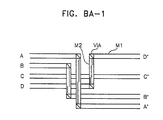
- a simple dual metal layout wherein vias are positioned at the locations of the desired direction changes is shown in Fig. BA - l, wherein the horizontal strips are typically a metal I layer, indicated as Ml, the vertical strips are typically a metal II layer, indicated as M2, and the vias interconnecting the two layers are labeled.
- the metal II layer overlies the metal I layer.
- Fig. BA - 2 In order to permit rapid customization of dual metal type integrated circuits, it is desired that such customization be solely produced by fuse disconnection rather than by applying metal across a gap. Accordingly, configurations such as that shown in Fig. BA - 2 were developed to combine the advantages of automatic routing with those of rapid customization, such that customization can be carried out by an automatic routing technique.
- the North-South strips are indicated to be metal I while the East-West strips are indicated to be metal II and a via connecting the metal I and metal II layers is disposed adjacent each crossing of the respective metal I and metal II strips.
- the via underlies the metal II strip and is joined to the metal I strip by means of a branch having a fuse formed thereon. Fuses are also provided along the metal II strips between adjacent vias and along the metal I strips between adjacent branches.
- Customization of the blank shown in Fig. BA - 2 takes place by traveling along the metal I strips and fusing all fuses on the branches which are not used. If a direction change is desired, a branch is used to establish a connection to the metal II layer. When traveling along the metal II strips, if the desired direction of the strip is, for example, West, the fuses lying to the East are fused or vice versa.
- Fig. BA - 3 illustrates the equivalent circuit to that shown in Fig. BA - l embodied in the structure of Fig. BA - 2, where /'s over the fuse indicate fused fuses.
- U.S. Patent 4,197,555 to Uehara describes a structure in which a relatively long strip of M1 is used. Although this structure is adequate for PAL configuration applications, it is relatively unsuitable for gate array applications, particularly if an automatic place-and-route program is used. Also, the length of the M1 strip acts to increase the line capacitance.
- the present invention seeks to provide selectably customizable semiconductor devices of the types described above which are compact and thus compatible with high-density architecture, and is useful inter alia in gate array technology and particularly in CMOS gate array technology.
- a selectably customizable semiconductor device including a first metal layer disposed in a first plane and including first elongate strips extending parallel to a first axis, a second metal layer disposed in a second plane generally parallel to and electrically insulated from the first plane and including second elongate strips extending parallel to a second axis, the second axis being generally perpendicular to the first axis, whereby a multiplicity of elongate strip overlap locations are defined at which the elongate strips of the first and second metal layers overlap in electrical insulating relationship, the first metal layer including a plurality of fusible conductive bridges joining adjacent pairs of the first elongate strips, the fusible conductive bridges including first and second fusible links, the first metal layer also including a plurality of branch strips, each branch strip connecting one of the fusible conductive bridges at a location intermediate the first and second fusible links to a branch overlap location spaced from the multiplicity of
- the selectably customizable semiconductor device also includes a fusible link formed on each strip of each of the pair of adjacent first elongate strips intermediate each pair of adjacent fusible conductive bridges.
- the selectably customizable semiconductor device also includes a fusible link formed on each of the second elongate strips intermediate each pair of adjacent branch overlap locations.
- a selectably customizable semiconductor device including a first metal layer disposed in a first plane and including first elongate strips extending parallel to a first axis, a second metal layer disposed in a second plane generally parallel to and electrically insulated from the first plane and including second elongate strips extending parallel to a second axis, the second axis being generally perpendicular to the first axis, whereby a multiplicity of elongate strip overlap locations are defined at which the elongate strips of the first and second metal layers overlap in electrical insulating relationship, the first metal layer including a plurality of fusible conductive bridges joining adjacent pairs of the first elongate strips, the fusible conductive bridges including first and second fusible links, an electrical connection being formed between the first metal layer and the second metal layer at a plurality of branch overlap locations, the branch overlap locations being disposed along a fusible conductive bridge intermediate the first and second fusible links and overlapping the second
- the first metal layer is a metal I layer and the second metal layer is a metal II layer.
- the first metal layer is a metal II layer and the second metal layer is a metal I layer.
- the selectably customizable semiconductor device also includes a fusible link formed on each strip of the pair of adjacent first elongate strips intermediate each pair of adjacent fusible conductive bridges.
- the selectably customizable semiconductor device also includes a fusible link formed on each of the second elongate strips intermediate each pair of adjacent branch overlap locations.
- a selectably customizable semiconductor device including a first metal layer disposed in a first plane and including first elongate strips extending parallel to a first axis, a second metal layer disposed in a second plane generally parallel to and electrically insulated from the first plane and including second elongate strips extending parallel to a second axis, the second axis being generally perpendicular to the first axis, whereby a multiplicity of elongate strip overlap locations are defined at which the elongate strips of the first and second metal layers overlap in electrical insulating relationship, the first metal layer including a plurality of fusible conductive bridges joining adjacent pairs of the first elongate strips, the fusible conductive bridges including first and second fusible links, an electrical connection being formed between the first metal layer and the second metal layer at a plurality of branch overlap locations, the branch overlap locations being disposed along a fusible conductive bridge intermediate the first and second fusible links and overlapping the second
- the selectably customizable semiconductor device also includes a third fusible link formed on each strip of the pair of adjacent first elongate strips intermediate each pair of adjacent fusible conductive bridges.
- a third link is formed on each strip of the pair of adjacent first elongate strips at each fusible conductive bridge. Additionally in this embodiment of the invention the third fusible link is disposed adjacent to each of the first and second fusible links.
- the selectably customizable semiconductor device also includes a fusible link formed on each of the second elongate strips intermediate each pair of adjacent branch overlap locations.
- all of the fusible links are formed in the second metal layer.
- the structure wherein all of the fusible links are formed in the second metal layer is suitable for gate array flexible routing.
- no prepatterning of the second metal layer is required to enable one step personalization to be carried out.
- the first and second elongate strips are arranged in a regular grid pattern.
- the first metal layer is a metal II layer and the second metal layer is a metal I layer.
- a method for selectably customizing a customizable semiconductor device including the steps of providing a selectably customizable semiconductor device as described above, and selectably fusing some of the plurality of fusible links.
- the selectably fusing step includes applying laser radiation to some of the plurality of fusible links.
- the selectably fusing step includes chemically etching some of the plurality of fusible links.
- the selectably fusing step includes ion milling some of the plurality of fusible links.
- the method of fusing includes the step of selectable fusing of fusible links on the second metal layer only. This technique does not require any holes to be formed in insulating layers underlying the second metal layer and enables personalization to be carried out without any change in the fabrication process.
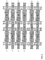
- FIG. 1 illustrates a metal on metal structure of a gate array constructed and operative in accordance with a preferred embodiment of the present invention.
- the structure of Fig. 1 is similar to that shown in Fig. BA - 2 but provides sharing of vias by two adjacent strips. This arrangement has been found to be highly effective in providing enhanced compactness. For convenience in description, directions East, West, North and South are defined on Fig. 1 and the remaining figures. These designations have no other significance and do not indicate any preferred orientation of the gate array or of the metal structure thereof.
- a first metal layer l0 typically metal I
- a second metal layer 14 typically metal II
- the second metal layer comprises a plurality of parallel elongate strips l6, extending East-West.
- Interconnecting adjacent pairs of elongate strips l2 are a plurality of branch strips 20. Formed on each of branch strips 20 are a pair of fusible links 22 and 24. Intermediate the fusible links 22 and 24 there is provided a branch link 25 which extends to a location underlying a strip l6, termed a branch overlap location and indicated by reference numeral 26. It is noted that branch overlap locations 26 are not found at elongate strip overlap locations l8.
- each branch overlap location 26 there is defined a via 28, providing electrical communication between the branch link 25 and the elongate strip 16.
- fusible links 30 are provided along strip 16 between adjacent pairs of strips l2.
- Fusible links 32 are provided along strips l2 between adjacent strips l6.
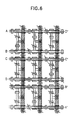
- FIG. 6 illustrates the structure of Fig. 1 which has been customized to correspond to the circuit layout of Fig. BA - l. Fuses which have been fused are shown with a superimposed /.
- a first metal layer 40 is disposed in the plane of the paper and comprises a plurality of parallel elongate strips 42, extending North-South.
- a second metal layer 44 is disposed in a plane generally parallel to the plane of the first metal layer and is electrically insulated therefrom.
- the second metal layer comprises a plurality of parallel elongate strips 46, extending East-West.
- Interconnecting adjacent pairs of elongate strips 46 are a plurality of branch strips 50. Unlike branch strips 20 of the embodiment of Fig. 1, here the branch strips are not straight but rather bend, defining a pair of bent arms extending across strips 42. Formed on each of branch strips 50 are a pair of fusible links 52 and 54. Intermediate the fusible links 52 and 54 is the location where the branch strip underlies a strip 42, this location being termed a branch overlap location and being indicated by reference numeral 56. It is noted that branch overlap locations 56 are not found at elongate strip overlap locations 48.
- each branch overlap location 56 there is defined a via 58, providing electrical communication between the branch 50 and the elongate strip 42.
- fusible links 60 are provided along strips 46 between adjacent pairs of strips 42.
- Fusible links 62 are provided along strips 42 between adjacent strips 46.
- branch overlap locations 56 overlapping adjacent parallel elongate strips are offset from each other such that they are not all aligned along a single line extending perpendicular to said parallel elongate strips.
- Fig. 2 The structure of Fig. 2 is particularly useful when, due to the requirements of fabrication technology, the size of the vias is relatively large. In such a case a particularly compact result is achieved by offsetting the adjacent vias.
- FIG. 5 illustrates the structure of Fig. 2 which has been customized to correspond to the circuit layout of Fig. BA - l. Fuses which have been fused are shown with a superimposed /.
- a first metal layer 70 typically metal II
- a second metal layer 74 typically metal I
- the second metal layer comprises a plurality of parallel elongate strips 76, extending East-West.
- Interconnecting adjacent pairs of elongate strips 72 are a plurality of branch strips 80. Unlike branch strips 20 of the embodiment of Fig. 1 and branch strips 60 of the embodiment of Fig. 3 here the branch strips are straight and extend in overlapping relationship with strips 76.
- branch strips 80 Formed on each of branch strips 80 are a pair of fusible links 82 and 84. Intermediate the fusible links 82 and 84 is a branch overlap location indicated by reference numeral 86. It is noted that branch overlap locations 86 are not found at elongate strip overlap locations 78.
- each branch overlap location 86 there is defined a via 88, providing electrical communication between the branch 80 and the elongate strip 76.
- fusible links 90 are provided along strip 76 between adjacent pairs of strips 72.
- Fusible links 92 are provided along strips 72 between adjacent strips 76.
- Fig. 3 The structure of Fig. 3 is highly compact but requires the ability to fuse a metal II fuse without disturbing an underlying metal I strip.
- FIG. 4 illustrates the structure of Fig. 3 which has been customized to correspond to the circuit layout of Fig. BA - l. Fuses which have been fused are shown with a superimposed /.
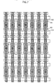
- FIG. 7 illustrates an even more compact grid array than that shown in Fig. 3.
- the arrangement is identical to that of Fig. 3 with the exception that fuses 92 are eliminated and replaced by fuses 102 which are located on strips 72 in overlying relationship with strips 76, adjacent to respective fuses 82 and 84. It will be appreciated that whenever a fuse 92 is fused, the adjacent fuse 82 or 84 will already have been fused.
- Fig. 7 has a number of advantages: All of the fusible links are aligned along strips 76.
- the elimination of fuses 92 enables the strips 76 to be brought closer to each other, so that the entire layout is more compact.
- the alignment of all of the fusible links along given lines enables relatively easy arrangement of a multi-metal layer arrangement.
- Fig. 7 also has a disadvantage in somewhat limiting the possible routing arrangements which can be realized by the layout, as compared with the embodiment of Fig. 3.
- FIG. 8 illustrates the structure of Fig. 7 which has been customized to correspond to the circuit layout of Fig. BA - l. Fuses which have been fused are shown with a superimposed /.
- Fig. 9 illustrates a somewhat simplified and less compact grid array than that shown in Fig. 3, wherein the shared vias of the configuration of Fig. 3 are eliminated and branches 80 do not interconnect adjacent strips 72. It is noted that the particular fuse arrangement of Fig. 7, wherein a fuse on one metal layer overlaps another metal layer, may be incorporated in the embodiment of Fig. 9. Every second strip 72 is eliminated. The arrangement of Fig. 9 has a disadvantage in somewhat decreased compactness, as compared with the embodiment of Fig. 3.
- FIG. 10 illustrates the structure of Fig. 9 which has been customized to correspond to the circuit layout of Fig. BA-1. Fuses which have been fused are shown with a superimposed /.
- Fig. 11 illustrates a structure wherein all of the fusible links normally used in personalization are formed on the metal II layer.
- the metal I layer is embodied in strips 150 extending vertically, which are not continuous but rather comprise a plurality of segments 180 disposed collinearly and in a mutually spaced relationship defining gaps 184 therebetween.
- the length of the segments l80 does not exceed about ten times the periodic spacing A of adjacent strips, as indicated in Fig. 11.
- the metal II layer comprises paired strips 152 extending generally perpendicularly to strips 150. Typically, each metal I segment 180 intersects with the projection onto the metal I plane of a single pair of strips 152. Each of paired strips 152 is connected to an adjacent strip 152 of an adjacent pair by metal II spurs 154 which overlie portions of the metal I strips 150.
- the metal I and metal II layers are interconnected by vias 156 extending between metal II spurs 154 and metal I segments 180.
- Fusible links in the metal II layer are indicated by reference numerals 158 and 160.
- each metal II spur 154 there are provided along each metal II spur 154 the following elements in the following order: a link 160, a via 156, a link 158 overlying a gap 184, another via 156, another link 160.
- Fusing of a link 158 thus prevents direct electrical communication between the metal I segments 180 on either side of the projection of link 158 onto the metal I plane.
- Fusing of a link 160 prevents direct electrical communication between the metal I segment 180 underlying the link 160 and the metal II strip adjacent the link 160.
- Fig. 12 illustrates the structure of Fig. 11 which has been customized to correspond to the circuit layout of Fig. BA - l. Fuses which have been fused are shown with a superimposed /. The resulting routing is shown by a thin line extending along the mid-line of the various strips of metal. When the routing is along metal I, the line is indicated as a solid line and when the routing is along metal II, the line is indicated as a dashed line.
- FIG. 13 illustrates a further alternative embodiment of the structure of Fig. 11 wherein a connection 170, provided with an additional fusible link 172 therealong, is interposed between adjacent collinear metal II spurs, thus linking the paired metal II strips 152 on either side of the link 172.
- Similar reference numbers are employed to show similar elements of the structure.
- This configuration is useful, as explained hereinbelow with reference to Fig. 14, in that it introduces redundancy along certain portions of the circuit layout, the transmission through which portions would otherwise be dependent upon passage through a via. This is advantageous because signals passing through vias involve higher resistivity and have lower yields.
- Fig. 14 illustrates the structure of Fig. 13 which has been customized to correspond to the circuit layout of Fig. BA - l. Fuses which have been fused are shown with a superimposed /. The resulting routing is shown by a thin line extending along the mid-line of the various strips, using the same format as described above in connection with Fig. 12. It may be seen that, e.g. in the final portion of the route of signal D from point D to point D′, the via dependent route of the signal along the metal I segment 180 on the far right is "backed up" by a parallel overlying non via-dependent route through a connection 170 adjacent the endpoint of the route of signal D.
- the present invention may be embodied by providing, preferably by mass production, metal I and metal II layers and a via layer therebetween, all patterned in accordance with a selected one of the configurations described hereinabove, and then personalizing the device for specific applications by a link-fusing process.
- metal I and metal II layers and a via layer therebetween all patterned in accordance with a selected one of the configurations described hereinabove, and then personalizing the device for specific applications by a link-fusing process.
- only the metal I layer and via layer may be provided, patterned in accordance with a selected one of the configurations described hereinabove, and may be covered with an unpatterned, uniform metal II layer.
- the fabrication up to this point is preferably effected by mass production techniques. Personalization for a particular desired application is then effected by patterning the metal II layer in accordance with the selected configuration described hereinabove.
- fusible links in the configuration which are to be fused need not be provided but rather may be replaced by gaps. It is appreciated that this alternative embodiment is only possible when the configurations of the metal I and metal II layers are such that no fusing of the metal I layer is required for personalization, as in the configurations disclosed herein with reference to Figs. 11, 13 and 15.
- metal I and metal II layers need not, in fact, be made specifically of metal, but rather may be formed from any suitable electrically conducting material.
Landscapes
- Design And Manufacture Of Integrated Circuits (AREA)
- Semiconductor Integrated Circuits (AREA)
Priority Applications (1)
| Application Number | Priority Date | Filing Date | Title |
|---|---|---|---|
| EP00102618A EP1011145A3 (de) | 1988-04-25 | 1989-04-24 | Abänderungsfähige Halbleiteranordnungen |
Applications Claiming Priority (4)
| Application Number | Priority Date | Filing Date | Title |
|---|---|---|---|
| IL86162 | 1988-04-25 | ||
| IL86162A IL86162A (en) | 1988-04-25 | 1988-04-25 | Customizable semiconductor devices |
| US222514 | 1988-07-21 | ||
| US07/222,514 US4933738A (en) | 1988-04-25 | 1988-07-21 | Customizable semiconductor devices |
Related Child Applications (1)
| Application Number | Title | Priority Date | Filing Date |
|---|---|---|---|
| EP00102618A Division EP1011145A3 (de) | 1988-04-25 | 1989-04-24 | Abänderungsfähige Halbleiteranordnungen |
Publications (2)
| Publication Number | Publication Date |
|---|---|
| EP0339534A2 true EP0339534A2 (de) | 1989-11-02 |
| EP0339534A3 EP0339534A3 (de) | 1990-11-07 |
Family
ID=26321794
Family Applications (1)
| Application Number | Title | Priority Date | Filing Date |
|---|---|---|---|
| EP19890107334 Ceased EP0339534A3 (de) | 1988-04-25 | 1989-04-24 | Abänderungsfähige Halbleiteranordnungen |
Country Status (2)
| Country | Link |
|---|---|
| EP (1) | EP0339534A3 (de) |
| JP (1) | JP2944100B2 (de) |
Cited By (4)
| Publication number | Priority date | Publication date | Assignee | Title |
|---|---|---|---|---|
| FR2718909A1 (fr) * | 1994-04-18 | 1995-10-20 | Transpac | Matrice de connexion configurable électriquement entre lignes d'au moins un port d'entrée-sortie de signaux électriques. |
| US5581098A (en) * | 1995-05-05 | 1996-12-03 | Circuit Integration Technology, Inc. | Circuit routing structure using fewer variable masks |
| US5907254A (en) * | 1996-02-05 | 1999-05-25 | Chang; Theodore H. | Reshaping periodic waveforms to a selected duty cycle |
| EP1063702A1 (de) * | 1999-05-21 | 2000-12-27 | International Business Machines Corporation | Sicherungsanordnung in einem Fenster mit doppelter Dichte |
Family Cites Families (8)
| Publication number | Priority date | Publication date | Assignee | Title |
|---|---|---|---|---|
| FR1503968A (fr) * | 1966-10-20 | 1967-12-01 | Constr Telephoniques | Perfectionnements aux matrices de circuits logiques intégrés |
| US4197555A (en) * | 1975-12-29 | 1980-04-08 | Fujitsu Limited | Semiconductor device |
| JPS5858809A (ja) * | 1981-09-30 | 1983-04-07 | 株式会社日立製作所 | ガス絶縁開閉装置 |
| JPS62165340A (ja) * | 1986-01-16 | 1987-07-21 | Toshiba Corp | 半導体装置の製造方法 |
| US4764800A (en) * | 1986-05-07 | 1988-08-16 | Advanced Micro Devices, Inc. | Seal structure for an integrated circuit |
| IL82113A (en) * | 1987-04-05 | 1992-08-18 | Zvi Orbach | Fabrication of customized integrated circuits |
| US4853758A (en) * | 1987-08-12 | 1989-08-01 | American Telephone And Telegraph Company, At&T Bell Laboratories | Laser-blown links |
| JPH01120843A (ja) * | 1987-11-05 | 1989-05-12 | Fujitsu Ltd | ウエーハスケール集積回路 |
-
1989
- 1989-04-24 EP EP19890107334 patent/EP0339534A3/de not_active Ceased
- 1989-04-25 JP JP1105735A patent/JP2944100B2/ja not_active Expired - Fee Related
Cited By (6)
| Publication number | Priority date | Publication date | Assignee | Title |
|---|---|---|---|---|
| FR2718909A1 (fr) * | 1994-04-18 | 1995-10-20 | Transpac | Matrice de connexion configurable électriquement entre lignes d'au moins un port d'entrée-sortie de signaux électriques. |
| EP0678948A1 (de) * | 1994-04-18 | 1995-10-25 | Transpac | Elektrisch konfigurierbare Matrix für Verbindungen zwischen Leitungen mit mindestens einem Ein/Ausgangstor für elektrische Signale |
| US5781124A (en) * | 1994-04-18 | 1998-07-14 | Transpac | Electrically configurable connection matrix between lines of at least one input/output port for electrical signals |
| US5581098A (en) * | 1995-05-05 | 1996-12-03 | Circuit Integration Technology, Inc. | Circuit routing structure using fewer variable masks |
| US5907254A (en) * | 1996-02-05 | 1999-05-25 | Chang; Theodore H. | Reshaping periodic waveforms to a selected duty cycle |
| EP1063702A1 (de) * | 1999-05-21 | 2000-12-27 | International Business Machines Corporation | Sicherungsanordnung in einem Fenster mit doppelter Dichte |
Also Published As
| Publication number | Publication date |
|---|---|
| JP2944100B2 (ja) | 1999-08-30 |
| JPH0215654A (ja) | 1990-01-19 |
| EP0339534A3 (de) | 1990-11-07 |
Similar Documents
| Publication | Publication Date | Title |
|---|---|---|
| US5049969A (en) | Customizable semiconductor devices | |
| US5619062A (en) | Personalizable gate array devices | |
| US5260597A (en) | Routing structure for a customizable integrated circuit | |
| US5679967A (en) | Customizable three metal layer gate array devices | |
| US4924287A (en) | Personalizable CMOS gate array device and technique | |
| US4568961A (en) | Variable geometry automated universal array | |
| US4197555A (en) | Semiconductor device | |
| TWI279882B (en) | Semi-custom-made semiconductor integrated circuit device, method for customization and method for redesign | |
| US20020024143A1 (en) | Semiconductor device | |
| US4720470A (en) | Method of making electrical circuitry | |
| JPH0572745B2 (de) | ||
| US4750027A (en) | Master slice semiconductor device | |
| JP3647323B2 (ja) | 半導体集積回路 | |
| US6093933A (en) | Method and apparatus for fabricating electronic device | |
| US5111273A (en) | Fabrication of personalizable integrated circuits | |
| EP0182222B1 (de) | Integrierte Halbleiterschaltungsanordnung in Polycell-Technik | |
| US5206184A (en) | Method of making single layer personalization | |
| EP0210397A1 (de) | LSI-Schaltungen, anwendbar bei kundenorientierten Entwurfsmethoden | |
| EP0339534A2 (de) | Abänderungsfähige Halbleiteranordnungen | |
| US5294754A (en) | Direct write EC single metal layer | |
| EP0021661A1 (de) | Masterslice-Halbleitervorrichtung | |
| EP0135019A2 (de) | Verbindung von Elementen auf ein Substrat mit integrierter Schaltung | |
| JPH04267553A (ja) | 半導体集積回路 | |
| EP0314376B1 (de) | Integriertes Schaltkreis-Bauelement vom Typ "Master Slice" und dessen Verwendung | |
| JPH0324763A (ja) | マスタスライス方式集積回路装置の形成方法 |
Legal Events
| Date | Code | Title | Description |
|---|---|---|---|
| PUAI | Public reference made under article 153(3) epc to a published international application that has entered the european phase |
Free format text: ORIGINAL CODE: 0009012 |
|
| AK | Designated contracting states |
Kind code of ref document: A2 Designated state(s): AT BE CH DE ES FR GB GR IT LI LU NL SE |
|
| RIN1 | Information on inventor provided before grant (corrected) |
Inventor name: AMIR, GIDEON Inventor name: JANAI, MEIR, I. Inventor name: YOELI, UZI Inventor name: ORBACH, ZVI |
|
| PUAL | Search report despatched |
Free format text: ORIGINAL CODE: 0009013 |
|
| AK | Designated contracting states |
Kind code of ref document: A3 Designated state(s): AT BE CH DE ES FR GB GR IT LI LU NL SE |
|
| 17P | Request for examination filed |
Effective date: 19910507 |
|
| RAP1 | Party data changed (applicant data changed or rights of an application transferred) |
Owner name: QUICK TECHNOLOGIES LTD. |
|
| 17Q | First examination report despatched |
Effective date: 19931201 |
|
| APAD | Appeal reference recorded |
Free format text: ORIGINAL CODE: EPIDOS REFNE |
|
| APAB | Appeal dossier modified |
Free format text: ORIGINAL CODE: EPIDOS NOAPE |
|
| APAB | Appeal dossier modified |
Free format text: ORIGINAL CODE: EPIDOS NOAPE |
|
| STAA | Information on the status of an ep patent application or granted ep patent |
Free format text: STATUS: THE APPLICATION HAS BEEN REFUSED |
|
| 18R | Application refused |
Effective date: 20000209 |
|
| APAF | Appeal reference modified |
Free format text: ORIGINAL CODE: EPIDOSCREFNE |