EP0339045B1 - Datenlimiter mit stromgesteuerter anlaufzeit - Google Patents
Datenlimiter mit stromgesteuerter anlaufzeit Download PDFInfo
- Publication number
- EP0339045B1 EP0339045B1 EP88900736A EP88900736A EP0339045B1 EP 0339045 B1 EP0339045 B1 EP 0339045B1 EP 88900736 A EP88900736 A EP 88900736A EP 88900736 A EP88900736 A EP 88900736A EP 0339045 B1 EP0339045 B1 EP 0339045B1
- Authority
- EP
- European Patent Office
- Prior art keywords
- signal
- analog
- output
- input
- data
- Prior art date
- Legal status (The legal status is an assumption and is not a legal conclusion. Google has not performed a legal analysis and makes no representation as to the accuracy of the status listed.)
- Expired - Lifetime
Links
- 230000004044 response Effects 0.000 title claims description 8
- 238000012545 processing Methods 0.000 claims abstract description 18
- 239000003990 capacitor Substances 0.000 claims description 28
- 238000004891 communication Methods 0.000 claims description 11
- 238000000034 method Methods 0.000 description 9
- 238000010586 diagram Methods 0.000 description 7
- 238000013459 approach Methods 0.000 description 6
- 230000006870 function Effects 0.000 description 6
- 230000001965 increasing effect Effects 0.000 description 4
- 230000008878 coupling Effects 0.000 description 3
- 238000010168 coupling process Methods 0.000 description 3
- 238000005859 coupling reaction Methods 0.000 description 3
- 230000009977 dual effect Effects 0.000 description 3
- 230000008901 benefit Effects 0.000 description 2
- 238000006243 chemical reaction Methods 0.000 description 2
- 238000012546 transfer Methods 0.000 description 2
- 230000007704 transition Effects 0.000 description 2
- 230000004913 activation Effects 0.000 description 1
- 230000015556 catabolic process Effects 0.000 description 1
- 230000008859 change Effects 0.000 description 1
- 230000003247 decreasing effect Effects 0.000 description 1
- 238000006731 degradation reaction Methods 0.000 description 1
- 230000001419 dependent effect Effects 0.000 description 1
- 238000013461 design Methods 0.000 description 1
- 230000000694 effects Effects 0.000 description 1
- 230000002708 enhancing effect Effects 0.000 description 1
- 238000005562 fading Methods 0.000 description 1
- 230000006872 improvement Effects 0.000 description 1
- 230000008569 process Effects 0.000 description 1
- 238000011084 recovery Methods 0.000 description 1
- 230000009467 reduction Effects 0.000 description 1
- 230000035945 sensitivity Effects 0.000 description 1
- 230000011664 signaling Effects 0.000 description 1
- 230000001360 synchronised effect Effects 0.000 description 1
Images


Classifications
-
- H—ELECTRICITY
- H03—ELECTRONIC CIRCUITRY
- H03M—CODING; DECODING; CODE CONVERSION IN GENERAL
- H03M1/00—Analogue/digital conversion; Digital/analogue conversion
- H03M1/12—Analogue/digital converters
- H03M1/124—Sampling or signal conditioning arrangements specially adapted for A/D converters
- H03M1/129—Means for adapting the input signal to the range the converter can handle, e.g. limiting, pre-scaling ; Out-of-range indication
- H03M1/1295—Clamping, i.e. adjusting the DC level of the input signal to a predetermined value
Definitions
- the present invention relates to communication receivers and more particularly to a data limiter circuit having a variable time constant for converting an analog signal to a digital signal.
- Communications systems in general and paging systems in particular using selective call signalling have attained widespread use for calling a selected paging system receiver by transmitting information from a base station transmitter to the paging receiver.
- Modern paging receivers have achieved multifunction capability through the use of microprocessors which allow the paging receiver to respond to information having various combinations of tone, tone and voice, or data messages. This information is transmitted using any number of paging coding schemes and message formats.
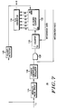
- FIG. 1 A block diagram of a prior art receiving system suitable for use in a synchronous paging system is illustrated in FIG. 1.
- the receiver comprises an antenna 10 which receives an RF signal and transmits it to a receiver 12 where the RF signal is amplified and converted into a first intermediate frequency (I.F.) signal by an RF amplifier and first mixer, respectively.
- I.F. intermediate frequency
- This I.F. signal is preferably directed to the receiver's backend where a first I.F. signal is converted to a second I.F. signal, in a dual conversion receiver, amplified, limited, demodulated, and filtered.
- the voltage level of the output signal at output 14 represents coded binary data or digital data.
- the output 14 of the receiver 12 is capacitively coupled to the input 15 of a data limiter 16 by way of a coupling capacitor 18 and bias resistor 17 connected between the differential inputs of the data limiter 16.
- the output 13 of the data limiter 16 is directed to a data processor 20 for further desired processing.
- the receiver system also includes one or more switches (normally transistors) connected between the various components of the receiver system and the power supply (B+).
- a switch 22 is periodically turned on and off under control of processor 20 by a battery saver routine 24 to provide a battery saving feature, which is a technique well known to those skilled in the art.
- a switch 26 (such as a transistor) is periodically closed to precharge the coupling capacitor 18, preferably by placing a resistor 27 in parallel with the limiter bias resistor 17 and input impedance, thereby reducing the overall RC time constant. Switch 26 is normally closed simultaneously with switch 22, but normally remains closed for a shorter time than switch 22 to provide this precharging.
- capacitor 18 will be a relatively large value in order to pass low frequency information and digital signals. Thus, a long time may be required to charge the capacitor 18, especially when it is connected to a high impedance such as the limiter bias resistor 17 for the data limiter 16. A long charge time necessitates the receiver "on" time being increased correspondingly to insure that capacitor 18 is charged to its correct bias point and that valid data is delivered to the data processor during the data decoding interval.
- the battery saver feature is clearly degraded by the extended receiver on time since this consumes more battery energy than is desirable.
- Switch 26 is used to alleviate this situation by providing a momentary low impedance charge path in parallel with the data limiter bias resistor 17 immediately upon receipt of power from the battery saver 24, that is, when the switch 22 is closed. This allows capacitor 18 to more rapidly charge to the bias voltage, depending upon the average value of the incoming data. If the incoming data can be depended upon to have no long strings of 1's or 0's, the charging of capacitor 18 will closely approximate the desired bias voltage. Data decoding of the received bit stream can begin more rapidly and continue until the battery voltage B+ is again removed by switch 22, thereby enhancing the battery saving feature.
- FIG. 2 there is shown, along with the battery saver strobe signal A, an input signal H, a threshold voltage G, and an output signal E of the prior art data limiter 16.
- the input signal H includes digital data modulated on the waveform.
- threshold signal G time t2
- data is detected and decoded as is illustrated in signal E. Note that even with precharging, data before time t2 is lost.
- the average voltage level at the output of the receiver will be at the desired carrier reference voltage, that is, the voltage level which corresponds to an undeviated RF signal.
- capacitor 18 will charge to a bias voltage which is consistent with this carrier reference voltage and proper data decoding will occur. If a long string of 1's or 0's is received immediately before the opening of switch 26, the average DC voltage of the receiver output 14 will be offset from the desired reference. The average DC voltage is increased if a large number of 1's are received or decreased if a large number of 0's are received.
- US-A-3 737 790 shows a noise-slicing device comprising a feedback loop with a comparator, an integrator for generating a reference signal and comprising a second comparator for producing the digital output depending on the analog input voltage and the reference signal.
- the gain in the loop is determined by a voltage divider at the output of the integrator.
- the present invention has been developed for the purpose of alleviating the above mentioned problems of the prior art. Accordingly, the invention has as one of its objects an apparatus and method for adjusting and controlling the time response of a data limiter in a communication receiver.
- a communication receiver for receiving coded information includes a receiving means, a data limiter, and a processing means.
- the receiving means receives the coded information including analog signals representative of digital data messages.
- the data limiter converts the analog signals to corresponding digital output signals to be applied to the processing means.
- the processing means receives and processes the digital data to provide data messages and alerts for the paging receiver's user.
- the processing means also controls the time constant of the data limiter and the storage of a comparison signal used for converting the analog signals to digital data.
- the data limiter having a variable time constant comprises an amplifying means, an integrating means, and a comparison means.
- the amplifying means having a variable bias current input, produces at its output terminal an analog reference signal from the analog input signal received at its input terminal, the analog reference signal being determined on the basis of the bias current input.
- the integrating means having a variable gain control produces at its output terminal an analog comparison signal from the analog reference signal, the analog comparison signal being determined on the basis of the gain.
- the comparison means responsive to the analog input signal and the analog comparison signal produces at its output a digital output signal depending on whether the amplitude of the analog input signal is larger or smaller than that of the analog comparison signal.
- the processing means produces a first, a second, and third control signals. The first control signal being applied to the amplifying means controls the bias current input.
- the second control signal being applied to the integrating means controls the gain.
- the third control signal being applied to the integrating means effects a storage of the analog comparison signal.
- FIG. 1 shows a battery saver receiver system of the prior art using a precharging technique to enhance response time.
- FIG. 2 shows waveforms useful in explaining the operation of the present invention and the prior art.
- FIG. 3 shows an overall block diagram of the present invention.
- FIG. 4 shows one embodiment of the data limiter of the present invention using only one transconductance amplifier.
- FIG. 5 shows a more detailed schematic of the diagram in FIG. 4.
- FIG. 6 shows a more detailed schematic of an analog circuit embodiment of the integrating means of the present invention.
- FIG. 7 shows a more detailed schematic of a digital circuit embodiment of the integrating means of the present invention.
- FIG. 8 shows another embodiment of the present invention including a transconductance amplifier and a comparator.
- FIG. 9 shows a more detailed schematic of the diagram of FIG. 8.
- an apparatus for providing a programmable data limiter having a variable current controlled response time While the present invention. is described hereinafter with particular reference to an FM communication receiver and in particular an FM paging receiver, it is to be understood at the outset of the description which follows that it is contemplated that the apparatus , in accordance with the present invention, may be used with other types of communication receivers.
- an antenna 10 provides receiver 12 with an input signal which is ultimately converted to a demodulated signal at receiver output 14 and delivered to data limiter 30.
- the output 14 from receiver 12 is applied to input 29 of the data limiter 30.
- Data limiter 30 includes at least one transconductance amplifier and integrating means 36.
- the output 31 from data limiter 30 is applied to an input 21 of a decoding means or processing means such as a data processor 20.
- Output 37 from data processor 20 is applied as a controlled input 39 to integrating means 36 of data limiter 30.
- the controlled input of integrating means includes a gain control 58 and a hold control 60.
- Gain control 58 controls the gain of integrating means 36.
- Hold control 60 effectively stores the output of integrating means 36.
- Another output from data processor 20 is applied to a digital to analog converter 32.
- the output 33 from digital to analog converter 32 controls bias current input 35 of a transconductance amplifier.
- digital data lines from processor 20 can replace analog output 33 to control the bias current of the transconductance amplifier.
- the data limiter circuit 30 can be controlled by output 33 or output 37 to control data limiter's 30 time constant (T1).
- T1 time constant
- the output 33 and 37 are programmed by the data processor 20 for tailoring the data limiter's 30 time constant to the particular bit pattern being received.
- input 35 can be set to zero, resulting in the comparison voltage D applied to the non-inverting input of the transconductance amplifier being stored in the integrating means 36.
- the comparison voltage can be stored by activation of a separate hold control 60.
- FIG. 2 illustrates waveforms which are helpful in explaining the operation of the data limiter circuit 30. It is to be understood that the waveforms are not exact but representative only.
- FIG. 2 shows the waveforms for a battery saver implementation of the present invention in which the paging receiver has been powered up and all power up transients have dissipated.
- Signal A is produced by the battery saver operation of the data processor.
- the decoding means or processor is operated in two modes; a high power drain mode when the battery saver strobe signal A is in the high "on” state; and a reduced power drain when the battery saver strobe signal A is in the low "off” state.
- the processor During the high state, the processor is in a fully operational mode in which it can decode signals in real time.
- the low portion of the battery saver strobe signal corresponds to a reduced computational ability mode in the data processor in which the data processor merely times the interval to the next transition to the high powered state.
- the time the data processor is fully operational or in a reduced power state depends upon the particular paging scheme employed by the paging system.
- Signal B illustrates data being received by the paging receiver during the "on" time of the battery saving strobe signal.
- the analog input signal B corresponds to the output 14 of receiver 12 which is applied to input 29 of data limiter 30.
- data is modulated on waveform B in a manner well known in the art.
- Signal H corresponds to the input voltage of data limiter 16 and signal G represents the data limiter 16 threshold voltage for the prior art shown in FIG. 1.
- Signal E corresponds to the output of the prior art data limiter. Since signal G decays each time the battery strobe is low and the prior art capacitor must be charged, the data is not detected until a time t2 for each battery saver strobe.
- One method to compensate for this is to start the battery saver strobe earlier at (-t2). However, this is undesired because it increases the drain on the battery.
- Signal D corresponds to the second input or analog comparison signal of data limiter 30 of the present invention. Since analog comparison signal D can be stored during the "off" interval, the data is decoded at an early time t1. As is evident, time t1 is a significant improvement over the prior art decoding of the data at time t2 (signal E). Additionally, since the time constant is programmable in data limiter 30, the time constant can be changed to cause comparison voltage D to track signal B for effectively decoding data during the battery saver strobe "on” interval. Thus, comparing output signal E and signal F which are the digital output signal of the decoded data of signal B, the advantages of the present invention are clearly seen.
- the time constant of the data limiter of the present invention can be controlled, the data can be decoded earlier during the operation of the paging receiver.
- the controlling of the time constant for the data limiter also allows an extremely long string of 1's or 0's to be decoded.
- the data limiter circuit 30 is adapted to have the time constant of the circuit controlled by an external means, such as data processor 20 also known as a decoding means.
- the integrating function performed by integrating means 36 can be performed by either analog or digital circuitry.
- the bias current input 35 or control input 39 can be programmed by decoding means 20 or other means for tailoring the data limiter time constant to the particular bit pattern being received. This optimizes performance by allowing an appropriate time constant to be used for each bit pattern and a resulting fast recovery from DC voltage shifts in the receiver output.
- bias current input 35 can be set to zero or alternatively the integrating means 36 can be programmed into a hold mode, resulting in the comparison voltage D being stored in the integrating means 36.
- the data limiter comparison voltage D is held during the time that the transmitted bit pattern is being decoded. This allows an extremely long string of 1's or 0's to be decoded.
- An example is an alphanumeric display paging receiver where a predetermined time constant is used until the paging receiver address is decoded, and then the comparison voltage D is stored by command from the processor means 20 for allowing a long alphanumeric message to be decoded. This message could be worst case all 1's or all 0's with no degradation due to loss of correct data limiter comparison voltage D. Also, the loss of data due to RF signal fading or channel interference is minimized.
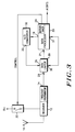
- FIG. 3 there is shown a schematic diagram for a paging receiver using the data limiter 30 of the present invention.
- An antenna 10 provides receiver 12 with an input signal which is ultimately converted to a demodulated signal at receiver output 14 and applied as input signal B to input 29 of data limiter 30.
- Data limiter 30 is adapted to have a programmable time constant which allows a comparison signal D to maintain an appropriate level for effectively decoding data of input signal B.
- the output 31 of data limiter 30 is applied to input 21 of data processor 20 for further processing.
- the receiver system includes one or more switches such as switch 22 connected between the various components of the receiver system and the power supply B+.
- a switch 22 is periodically turned on and off under control of processor 20 by a battery saver routine 24 to provide a battery saving feature, which is a technique well known to those skilled in the art.
- Another output from data processor 20 is applied to a digital to analog converter 32.
- the output 33 from digital to analog converter 32 controls the bias current input 35 of the data limiter 30.
- the data limiter circuit 30 can be controlled by the output 33 generated by the digital to analog converter 32 for controlling the data limiter 30 time constant (T1).
- T1 time constant
- the output 33 is programmed by the data processor for tailoring the data limiter time constant to the particular bit pattern being received.
- Another output 37 from data processor 20 is applied to an input 39 of data limiter 30.
- the input 39 includes a gain control and a hold control for the data limiter 30.
- the gain control provides a further controlling of the data limiter time constant as will be explained with reference to FIG. 4.
- the hold control allows the data limiter to selectively store the voltage comparison signal D for permitting the data limiter to effectively
- Data limiter 30 includes a differential input dual output transconductance amplifier 34 with a transconductance gain (gm) controlled by bias current Ibias applied to input 35.
- the output 14 of receiver 12 is applied to the non-inverting input 29 of amplifier 34.
- One current output 23 (I1) of amplifier 34 is applied to a high gain limiting transresistance amplifier 38.
- Amplifier 38 functions to convert the output current I1 to a limited voltage which is the digital output signal F of data limiter 30.
- the output of data limiter 30 is applied to an input 21 of data processor 20.
- the second output 25 (reference signal I2) of amplifier 34 is applied to one input 52 of integrating means 36. Integrating means 36 generates an output voltage (comparison signal D) which is the time integral of the input current I2.
- T1 is varied by means of Ibias or the integrating means gain to be large in comparison with the longest string of 1's or 0's in the binary bit pattern to be detected by the data limiter. If a binary bit pattern is applied to the data limiter input B, the limiter comparison voltage D attempts to track the input signal level but never reaches that level (except during transitions) due to the long time constant T1.
- the average current I2 into the integrating means 36 approaches zero. Since I1 and I2 are directly proportional, the average current into limiting amplifier 38 must also approach zero. Therefore, the data limiter circuit 30 input comparison voltage D is forced to a level which results in limiting about the average DC value of the incoming signal B. The limited output signal F appears at the output of amplifier 38. At any time, the comparison voltage D can be held and stored in the integrating means 36 by setting bias current Ibias to zero or by programming the integrating means 36 to a hold mode.
- the digital to analog converter 32 converts a digital output of data processor 20 to the bias current Ibias which controls transconductance amplifier 34 through a current source reference 120 in a manner well known in the art. In the simplest application, the digital to analog converter 32 can be a resistor connected to a digital voltage output of the data processor 20.
- Data processor 20 includes control lines 37 having a gain control output 54 and a hold control output 56.
- the gain control output 54 is applied to input 58 of integrating means 36 to control the gain of integrating means 36.
- the hold control signal 56 is applied to another input 60 of integrating means 36 for effecting a storage of the comparison voltage D from output 55 which is applied to the inverting input 27 of amplifier 34.
- data processor 20 controls the integrating means gain and the Ibias of transconductance amplifier 34, the data processor can effectively control the time constant of the data limiter 30 by varying the bias current Ibias or the integrating means gain.
- the hold control allows data processor 20 to effectively hold a comparison voltage D on input 27 of amplifier 34.
- data processor 20 programmably controls the time constant and the storing of the comparison voltage D of data limiter 30.
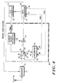
- FIG. 5 a more detailed representation of FIG. 4 is shown using integrated circuit design techniques.
- the voltage input B connected to input 29 is applied to the base of PNP transistor 100.
- the emitter of transistor 100 is connected to the emitter of PNP transistor 102, forming a differential amplifier configuration of amplifier 34.
- the bias current Ibias for amplifier 34 is connected to the emitters of transistor 100 and 102.
- a PNP transistor 104 having four collectors, has two of the collectors coupled to the emitters of transistors 100 and 102 for supplying the bias current.
- the emitter of transistor 104 is connected to B+, and the base is connected to a current source reference 120 which is connected to an output of the digital to analog converter 32.
- transistor 104 the remaining two collectors are connected to the bases of NPN transistors 106, 108, 110, and 112.
- the connection of transistor 104 forms a controllable current supply for the differential amplifier configuration of transistors 100 and 102 and the DC biased circuits formed by transistors 106 and 108 and transistors 110 and 112.
- Transistor 106 has its collector tied to its base and the emitter tied to ground.
- the collector of transistor 108 is connected to the collector of transistor 100 and further connected to the base of transistor 118.
- the emitter of transistor 108 is connected to ground.
- transistors 106 and 108 form a current mirror configuration providing a DC bias for transistor 100.
- transistor 110 one-fourth of the current from the collectors of 104 is applied to the bases of transistor 110 and 112.
- the collector of 110 is tied back to its base while the emitter is connected to ground.
- the collector is connected to the collector of transistor 102 while the emitter is connected to ground.
- Transistors 110 and 112 form a current mirror which provides a DC bias for transistor 102.
- the collectors of transistors 102 and 112 are further connected to a capacitor 114.
- the other end of capacitor 114 is connected to ground.
- the integrator in its simplest form includes the capacitor 114.
- the collectors of transistor 102 and 112 are further connected to the base of transistor 102. It is important to note that the base of transistor 102 is the inverting input 27 (comparison signal D) of amplifier 34.
- the collector of 118 is connected in series with a resistor 116 to the battery saver strobe, also known as signal A.
- the emitter of transistor 118 is connected to ground.
- the output of the data limiter 30 is connected to the collector of 118.
- transistor 118 is turned off, the output F is pulled toward the battery saver strobe voltage by resistor 116.
- the transistor is turned on, the output is coupled to ground, thereby pulling the output low.
- Transistor 118 is controlled by current I1 generated between the collectors of transistor 100 and 108.
- the transconductance amplifier includes the transistors 100-102, 106-112 transistors 100 and 102 forming a differential amplifier with transistors 106-112 providing biasing currents.
- the integrating means 36 comprises capacitor 114 for performing the integrating function.
- the transresistance amplifier 38 includes transistor 118 and resistor 116.
- the voltage input B is applied to the base of transistor 100 and the digital output voltage F is taken from the collector of 118.
- the current source reference 120 controls the currents sourced by transistor 104 and the time constant of the data limiter.
- T1 4 (K) (T) (C) (q) ( Ibias)
- C Capacitance of capacitor 114
- K Boltzmann's constant
- T Temperature in degrees Kelvin
- q Electron charge
- the sensitivity of the data limiter circuit 30 to variations in PNP transistor beta can be reduced by taking output current I1 from transistor 102 instead of 100. This is accomplished by splitting the collector of transistor 102 into two collectors and using the added collector to drive the base of transistor 118. The collector of transistor 100 is then attached to ground and the collector of 108 is connected to the base of transistor 118. For a given current Ibias, the bias circuits being sinked by transistors 108 and 112 would require reduction by 50 percent when this change is made. The data limiter time constant would then be increased by a factor of 2.
- the analog integrator circuit shown in FIG. 6 includes capacitor 114 for integrating the input current I2 and generating the comparison voltage D.
- a buffer amplifier 122 having a fixed or variable gain (K2) may be connected between capacitor 114 and output 55.
- the buffer amplifier 122 improves performance of the circuit by minimizing loading on capacitor 114.
- the variable gain buffer amplifier 122 allows the gain of integrating means 36 to be controlled by data processor 20.
- the digital integrating circuit of FIG. 7 includes an absolute value circuit 124 connected to the output 25 of amplifier 34.
- the absolute value circuit 124 is connected to a current controlled oscillator 126.
- the absolute value circuit 124 is used to transform a positive or negative input current I2 into a positive current for driving the current controlled oscillator 126.
- the input current I2 could be converted to a voltage before being applying to the absolute value circuit 124.
- a voltage controlled oscillator would then be used.
- the oscillator 126 generates an output frequency which is directly proportional to the input current I2. To optimize performance, the oscillator digital output signal is latched at the last level whenever the input current is zero or near zero.
- the output from the oscillator 126 is applied to one input of an AND gate 128.
- the other input of the AND gate 128 is tied to the hold control signal from the data processor means.
- the output from AND gate 128 is applied to an input of a programmable divide by N counter 130.
- the AND gate 128 causes the integrator output voltage (comparison voltage D) to be stored whenever the hold signal is activated from the data processor.
- the programmable counter 130 controls the integrator gain with one or more inputs from an external source.
- the AND gate 128 and programmable counter 130 are optional and not required for the basic operation of the integrating means.
- the output of the programmable counter 130 drives the up/down counter 132 which in turn drives the digital to analog converter 134.
- the direction that the up/down counter will count is controlled by the digital signal derived from a polarity detector 125 responsive to the integrator input current I2.
- the polarity detector 125 causes the counter 132 to count in a direction that results in an increasing digital to analog converter output voltage D.
- FIG. 7 illustrates a 6 bit digital to analog converter, other size converters can be used.
- a digital value for comparison voltage D can be maintained in counter 132 even though power is removed from the other circuitry of integrating means 36.
- the up/down counter 132 can also be powered down if the binary pattern in the up/down counter 132 is temporarily stored elsewhere such as in the data processor.
- K3 Gain of integrator not including programmable counter
- the digital integrator circuit of FIG. 7 shows one method for providing a programmable gain for the integrating means to control the time constant of the data limiter.
- the time constant of the data limiter can be easily controlled through programming the data processor 20.
- FIG. 8 a second embodiment of the data limiter circuit is shown.
- the circuit of FIG. 8 is similar to the data limiter circuit in FIG. 4.
- the dual output transconductance amplifier 34 and amplifier 38 of FIG. 4 has been replaced by a voltage comparator 40 and a single ended transconductance amplifier 42.
- the input voltage B is applied simultaneously to the non-inverting input 47 of comparator 40 and the non-inverting input 41 of transconductance amplifier 42.
- the output from integrating means 36 is connected to the inverting input 44 of transconductance amplifier 42 and the inverting input 46 of comparator 40.
- the output from comparator 40 is the binary output signal F which is applied to input 21 of data processor 20.
- the digital to analog converter 32 controls the bias current (Ibias) for transconductance amplifier 42.
- the circuit in FIG. 8 allows the data limiter control current Ibias to be reduced to zero or near zero without losing the data limiter output signal F. Before in FIG. 4, when the Ibias current was reduced to zero, this eliminated the driving current 11 for the transresistance amplifier 38 with a resultant loss in data limiter output signal F. It is important to note that in FIG. 4, Ibias is turned to zero only when the battery saver strobe signal is turned "off". However, the data limiter circuit of FIG. 8 allows the data limiter control current Ibias to be reduced to zero or near zero without losing the data limiter output signal F.
- the input signal B is compared to voltage comparison signal D at voltage comparator 40. If voltage B is greater than voltage D, the output 31 from comparator 40 is at a high level. If voltage B is less than voltage D, the output 31 from comparator 40 is at a low level.
- To generate voltage comparison signal D input signal B is applied to the non-inverting input 41 while the output 55 of integrating means 36 is applied to the inverting input 44 of amplifier 42.
- the output 55 (comparison voltage D) tracks the input signal B with an exponential time constant T1 as described in reference to FIG. 4.
- the comparison signal D is then fed back to the amplifier 42 and used as a comparison signal in comparator 40.
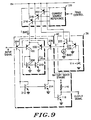
- FIG. 9 there is shown a detailed schematic diagram of the data limiter as shown in FIG. 8.
- the phantom lines show the components of the comparator 40, amplifier 42, integrating means 36, and current source reference 120. It is to be understood that the phantom lines showing the components of amplifier 42 are not included in the components for comparator 40.
- the transconductance amplifier 42 includes PNP transistors 200 and 202 and NPN transistors 208 and 210.
- the voltage comparator 40 includes PNP transistors 204 and 206 and NPN transistors 118, 212, and 214 in addition to resistor 116.
- the integrating means for generating comparison voltage D includes capacitor 114, NPN transistor 222, and PNP transistor 224.
- the voltage input B is applied to the base of transistors 204 and 200.
- the comparison voltage D is applied to the base of transistors 202 and 206.
- the output from the data limiter is taken from the collector of transistor 118.
- the current source reference 120 controls the bias current (Ibias) applied to the transconductance amplifier 42 by way of PNP transistor 216, to the voltage comparator 40 by way of PNP transistor 218, and to the integrator by way of PNP transistor 220.
- the emitters for transistors 216-220 are connected to B+.
- the collector for transistor 216 is connected to the emitters of transistors 200 and 202.
- the collector for transistor 218 is connected to the emitters of transistors 204 and 206.
- the collector of transistor 220 is connected to the emitter of transistor 224 and the base of 222.
- transistor 216 provides the bias for the transconductance amplifier 42.
- Transistor 218 provides the bias current for the voltage comparator.
- Transistor 220 provides bias current for the integrating means 36.
- the collector of transistor 200 is connected to the base of transistor 208 and transistor 210.
- the collector of 208 is connected back to the base of 208.
- the emitter of transistor 208 is connected to ground.
- the emitter of transistor 210 is connected to ground with the collector of transistor 210 connected to the collector of transistor 202 and the capacitor 114 and the base of transistor 224.
- the other end of capacitor 114 is connected to ground.
- transistors 208 and 210 form a current mirror circuit for the transconductance amplifier 42.
- the output of the transconductance amplifier 42 is formed at the junctions of the collectors 210 and 202 and is applied to the capacitor 114 and to the base of transistor 224.
- the collector of transistor 224 is connected to ground and the emitter is connected to the collector of 220 and the base of transistor 222.
- the collector of transistor 222 is connected to B+ with the emitter connected to the base of transistor 206 and a current source 226.
- transistors 222 and 224 form a high input impedance buffer amplifier which minimizes loading on capacitor 114.
- the collector of transistor 204 is connected to the bases of transistor 212 and 214, transistor 212 having its collector connected back to its base and its emitter connected to ground.
- Transistor 214 has its emitter connected to ground and its collector connected to the collector of transistor 206.
- the collectors of transistors 206 and 214 are connected to the base of transistor 118.
- the connection of transistor 118 has been previously explained with reference to FIG. 5 and is not repeated here.
- the output of comparator 40 is the collector of transistor 118.
- the output of the comparator 40 is voltage output F which is applied to the data processor 20. The operation of the transconductance amplifier and the voltage comparator circuit have been explained with reference to FIG. 8 and will not be repeated here.
- the circuit of FIG. 9 provides the ability to control the bias currents individually for the voltage comparator 40, the transconductance amplifier 42, and the buffer of integrating means 14.
- the transistors 216-220 can be switched off during battery saver off interval for minimizing current drain.
- Transistor 216 providing the bias current for the transconductance amplifier, can be switched off during the battery saver on interval for storing the comparison voltage C while maintaining a valid data limiter output signal F.
- T1 (2) (K) (T) (C) (q) (Ibias)
Landscapes
- Engineering & Computer Science (AREA)
- Theoretical Computer Science (AREA)
- Circuits Of Receivers In General (AREA)
- Mobile Radio Communication Systems (AREA)
- Control Of Ac Motors In General (AREA)
- Control Of Amplification And Gain Control (AREA)
Claims (10)
- Datenlimiter in einem Kommunikationsempfänger, wobei der Kommunikationsempfänger eine Verarbeitungseinrichtung (20) aufweist, und der Datenlimiter eine variable Zeitkonstante aufweist, um ein analoges Eingangssignal in ein digitales Ausgangssignal (F) umzuwandeln, und der Datenlimiter umfaßt:
eine Verstärkungseinrichtung (42), welche einen variablen Vorspannungsstromeingang (35) aufweist, um an ihrer Ausgangsanschlußklemme (25) ein analoges Bezugssignal aus dem analogen Eingangssignal (B), welches an ihrer ersten Eingangsklemme (41) empfangen wird, und aus einem analogen Vergleichssignal (D), welches an ihrer zweiten Eingangsklemme (44) empfangen wird, zu erzeugen, wobei das analoge Bezugssignal auf der Grundlage des Vorspannungsstrom-Eingangssignals (35) festgelegt wird;
eine Integriereinrichtung (36), die einen Steuereingang (58) mit variabler Verstärkung aufweist, um an ihrer Ausgangsklemme (55) das analoge Vergleichssignal (D) aus dem analogen Bezugssignal zu erzeugen, wobei das analoge Vergleichssignal (D) auf der Grundlage der Verstärkung der Integriereinrichtung (36) festgelegt wird; und
eine Vergleichseinrichtung (40) zur Erzeugung des digitalen Ausgangssignals (F) an ihrem Ausgang, abhängig von der Differenz zwischen dem analogen Vergleichssignal (D) und dem analogen Eingangssignal (B),
wobei die Verarbeitungseinrichtung (20) ein erstes Steuersignal und ein zweites Steuersignal (GAIN) erzeugt, die Verstärkungseinrichtung (42) auf das erste Steuersignal reagiert, um das Vorspannungsstrom-Eingangssignal zu modifizieren, und die Integriereinrichtung (36) auf das zweite Steuersignal reagiert, um die Verstärkung zu modifizieren, wodurch das analoge Bezugssignal durch das Vorspannungsstrom-Eingangssignal (35) und das Verstärkungseingangssignal (58) geändert wird. - Datenlimiter nach Anspruch 1, bei welchem die Vergleichseinrichtung ein digitales Ausgangssignal erzeugt, abhängig davon, ob die Amplitude des analogen Eingangssignals größer oder kleiner als die des analogen Vergleichssignals ist.
- Datenlimiter nach Anspruch 2, bei welchem die Integriereinrichtung eine Speichereinrichtung zum Speichern des analogen Vergleichssignals aufweist.
- Datenlimiter nach Anspruch 3, bei welchem die Verarbeitungseinrichtung ein drittes Steuersignal (HOLD) aufweist, welches an die Integriereinrichtung angelegt wird, um das Speichern des analogen Vergleichssignals zu steuern.
- Datenlimiter nach Anspruch 3, bei welchem die Speichereinrichtung einen Kondensator (114) aufweist.
- Datenlimiter nach Anspruch 3, bei welchem die Integriereinrichtung eine digitale Integrierschaltung aufweist.
- Datenlimiter nach Anspruch 6, bei welchem die digitale Integrierschaltung aufweist:
eine Absolutwertschaltung (124), die auf das analoge Bezugssignal reagiert, um einen Absolutwert des analogen Bezugssignals zu erzeugen;
einen Oszillator (126), der auf das absolute analoge Bezugssignal reagiert, um das absolute analoge Bezugssignal in eine entsprechende Frequenz umzuwandeln;
einen Zähler (130; 132), der auf das Ausgangssignal des Oszillators zur Erzeugung eines digitalen Zählwertes reagiert; und
einen Digital/Analog-Wandler (134) zur Umwandlung des digitalen Zählwertes des Zählers in das analoge Vergleichssignal. - Datenlimiter nach Anspruch 7, bei welchem der Zähler aufweist:
eine Gate-Einrichtung (128), die auf das Ausgangssignal des Oszillators und das dritte Steuersignal reagiert, um selektiv das Ausgangssignal des Oszillators anzulegen;
einen programmierbaren Zähler (130), der auf das Ausgangssignal der Gate-Einrichtung reagiert, um einen Taktimpuls zu erzeugen, wobei der programmierbare Zähler weiterhin auf das zweite Steuersignal (GAIN) reagiert, um selektiv den Taktimpuls anzulegen; und
einen zweiten Zähler (132), der auf die Taktimpulse reagiert, um einen digitalen Zählwert abhängig von einer Polarität des analogen Bezugssignals zu erzeugen. - Datenlimiter nach Anspruch 4, bei welchem das analoge Vergleichssignal in Reaktion auf die Beendigung der Stromversorgung gespeichert wird.
- Datenlimiter in einem Kommunikationsempfänger, wobei der Kommunikationsempfänger eine Verarbeitungseinrichtung (20) aufweist, und der Datenlimiter ein analoges Eingangssignal (B) in ein digitales Ausgangssignal (F) umwandelt, und der Datenlimiter umfaßt:
eine Verstärkungseinrichtung (42), die auf das analoge Eingangssignal (B) und ein Vergleichssignal (D) reagiert, um ein Ausgangsbezugssignal zu erzeugen, welches auf der Grundlage eines variablen Vorspannungsstroms festgelegt wird;
eine Integriereinrichtung (36), die auf das Ausgangsbezugssignal reagiert, um das Vergleichssignal (D) zu erzeugen, welches auf der Grundlage einer Verstärkung festgelegt wird; und
eine Vergleichseinrichtung (40), die auf das Vergleichssignal (D) und auf das analoge Eingangssignal (B) reagiert, um das digitale Ausgangssignal (F) zu erzeugen, abhängig von der Differenz zwischen dem analogen Eingangssignal (B) und dem Vergleichssignal (D),
wobei die Verarbeitungseinrichtung (20) ein Steuersignal erzeugt, wobei die Verstärkungseinrichtung (42), an welche der variable Vorspannungsstrom angelegt wird, auf das Steuersignal reagiert, um den variablen Vorspannungsstrom zu ändern, und
wobei die Verarbeitungseinrichtung (20) ein Verstärkungssignal erzeugt, um die Verstärkung der Integriereinrichtung (36) zu ändern, wodurch das Ausgangsbezugssignal durch den variablen Vorspannungsstrom und die Verstärkungssignale geändert wird.
Applications Claiming Priority (3)
| Application Number | Priority Date | Filing Date | Title |
|---|---|---|---|
| US27787A | 1987-01-02 | 1987-01-02 | |
| PCT/US1987/003294 WO1988005229A1 (en) | 1987-01-02 | 1987-12-14 | Data limiter with current controlled response time |
| US277 | 1995-06-16 |
Publications (3)
| Publication Number | Publication Date |
|---|---|
| EP0339045A1 EP0339045A1 (de) | 1989-11-02 |
| EP0339045A4 EP0339045A4 (en) | 1991-07-03 |
| EP0339045B1 true EP0339045B1 (de) | 1994-08-24 |
Family
ID=21690778
Family Applications (1)
| Application Number | Title | Priority Date | Filing Date |
|---|---|---|---|
| EP88900736A Expired - Lifetime EP0339045B1 (de) | 1987-01-02 | 1987-12-14 | Datenlimiter mit stromgesteuerter anlaufzeit |
Country Status (5)
| Country | Link |
|---|---|
| EP (1) | EP0339045B1 (de) |
| JP (1) | JPH02500076A (de) |
| AT (1) | ATE110501T1 (de) |
| DE (1) | DE3750429T2 (de) |
| WO (1) | WO1988005229A1 (de) |
Families Citing this family (1)
| Publication number | Priority date | Publication date | Assignee | Title |
|---|---|---|---|---|
| RU2195767C1 (ru) * | 2001-05-25 | 2002-12-27 | ОАО "Ульяновское конструкторское бюро приборостроения" | Устройство для преобразования напряжения переменного тока в код |
Family Cites Families (6)
| Publication number | Priority date | Publication date | Assignee | Title |
|---|---|---|---|---|
| US3214700A (en) * | 1961-03-17 | 1965-10-26 | Trw Inc | Variable threshold signal detection system |
| US3550018A (en) * | 1968-09-11 | 1970-12-22 | Bendix Corp | Digital integrator-synchronizer having low noise susceptibility |
| US3737790A (en) * | 1971-12-21 | 1973-06-05 | Us Navy | Noise-riding slicer |
| JPS58168314A (ja) * | 1982-03-30 | 1983-10-04 | Nec Corp | 自動利得制御増巾回路 |
| US4575863A (en) * | 1983-12-22 | 1986-03-11 | Motorola, Inc. | Fast recovery bias circuit |
| US4590394A (en) * | 1984-03-13 | 1986-05-20 | Motorola, Inc. | Signal processing circuit with voltage clamped input |
-
1987
- 1987-12-14 WO PCT/US1987/003294 patent/WO1988005229A1/en not_active Ceased
- 1987-12-14 JP JP63500958A patent/JPH02500076A/ja active Granted
- 1987-12-14 AT AT88900736T patent/ATE110501T1/de not_active IP Right Cessation
- 1987-12-14 EP EP88900736A patent/EP0339045B1/de not_active Expired - Lifetime
- 1987-12-14 DE DE3750429T patent/DE3750429T2/de not_active Expired - Fee Related
Also Published As
| Publication number | Publication date |
|---|---|
| DE3750429D1 (de) | 1994-09-29 |
| ATE110501T1 (de) | 1994-09-15 |
| JPH0522409B2 (de) | 1993-03-29 |
| JPH02500076A (ja) | 1990-01-11 |
| DE3750429T2 (de) | 1995-03-09 |
| EP0339045A4 (en) | 1991-07-03 |
| EP0339045A1 (de) | 1989-11-02 |
| WO1988005229A1 (en) | 1988-07-14 |
Similar Documents
| Publication | Publication Date | Title |
|---|---|---|
| US4866261A (en) | Data limiter having current controlled response time | |
| US5426389A (en) | System for DC restoration of serially transmitted binary signals | |
| US4929851A (en) | Data limiter for a radio pager | |
| EP0381371A2 (de) | Digitaler Datenempfänger mit Burst-Mode | |
| EP0326940B1 (de) | Phasenregelschleife mit einer Schaltung zur schnellen Verriegelung durch Verringerung und Begrenzung des Stromes | |
| US3986125A (en) | Phase detector having a 360 linear range for periodic and aperiodic input pulse streams | |
| US4590394A (en) | Signal processing circuit with voltage clamped input | |
| JPH06232917A (ja) | デジタルデータ受信機 | |
| KR100186859B1 (ko) | 데이터 복호회로, 전압 제어 발진회로, 데이터 복호장치 및 전자기기 | |
| KR860001241B1 (ko) | 직류 모우터 구동 집적회로 | |
| US4500844A (en) | Ringing signal generator employing delta-modulation power amplification techniques | |
| US4419760A (en) | Augmented phase-locked loop for very wide range acquisition and method therefor | |
| US4635280A (en) | Bit synchronizer for decoding data | |
| JPS6324572B2 (de) | ||
| US6219380B1 (en) | Pulse position modulation based transceiver architecture with fast acquisition slot-locked-loop | |
| US4156871A (en) | Analog-to-pulse density converter | |
| US3746990A (en) | Coder-decoder for use in a delta-transmission system | |
| EP0339045B1 (de) | Datenlimiter mit stromgesteuerter anlaufzeit | |
| US4881042A (en) | Automatically tunable phase locked loop FM detection system | |
| JPH07105118B2 (ja) | スレッショルドトラッキング方式 | |
| US3387296A (en) | Telemetering system | |
| US5365120A (en) | Data slicer with hold | |
| US5712475A (en) | Light receiving circuit with variable threshold circuit | |
| US5502746A (en) | Dual stage differential adaptive peak detector for data communications receivers | |
| EP0325391A3 (en) | Pseudo-ternary code transmitter |
Legal Events
| Date | Code | Title | Description |
|---|---|---|---|
| PUAI | Public reference made under article 153(3) epc to a published international application that has entered the european phase |
Free format text: ORIGINAL CODE: 0009012 |
|
| 17P | Request for examination filed |
Effective date: 19890626 |
|
| AK | Designated contracting states |
Kind code of ref document: A1 Designated state(s): AT BE CH DE FR GB IT LI LU NL SE |
|
| A4 | Supplementary search report drawn up and despatched |
Effective date: 19910515 |
|
| AK | Designated contracting states |
Kind code of ref document: A4 Designated state(s): AT BE CH DE FR GB IT LI LU NL SE |
|
| 17Q | First examination report despatched |
Effective date: 19930401 |
|
| ITF | It: translation for a ep patent filed | ||
| GRAA | (expected) grant |
Free format text: ORIGINAL CODE: 0009210 |
|
| AK | Designated contracting states |
Kind code of ref document: B1 Designated state(s): AT BE CH DE FR GB IT LI LU NL SE |
|
| PG25 | Lapsed in a contracting state [announced via postgrant information from national office to epo] |
Ref country code: NL Effective date: 19940824 |
|
| REF | Corresponds to: |
Ref document number: 110501 Country of ref document: AT Date of ref document: 19940915 Kind code of ref document: T |
|
| REF | Corresponds to: |
Ref document number: 3750429 Country of ref document: DE Date of ref document: 19940929 |
|
| PGFP | Annual fee paid to national office [announced via postgrant information from national office to epo] |
Ref country code: FR Payment date: 19941024 Year of fee payment: 8 |
|
| PGFP | Annual fee paid to national office [announced via postgrant information from national office to epo] |
Ref country code: CH Payment date: 19941027 Year of fee payment: 8 |
|
| PG25 | Lapsed in a contracting state [announced via postgrant information from national office to epo] |
Ref country code: SE Effective date: 19941124 |
|
| ET | Fr: translation filed | ||
| PGFP | Annual fee paid to national office [announced via postgrant information from national office to epo] |
Ref country code: BE Payment date: 19941209 Year of fee payment: 8 |
|
| PGFP | Annual fee paid to national office [announced via postgrant information from national office to epo] |
Ref country code: AT Payment date: 19941223 Year of fee payment: 8 |
|
| PG25 | Lapsed in a contracting state [announced via postgrant information from national office to epo] |
Ref country code: LU Free format text: LAPSE BECAUSE OF NON-PAYMENT OF DUE FEES Effective date: 19941231 |
|
| NLV1 | Nl: lapsed or annulled due to failure to fulfill the requirements of art. 29p and 29m of the patents act | ||
| PLBE | No opposition filed within time limit |
Free format text: ORIGINAL CODE: 0009261 |
|
| STAA | Information on the status of an ep patent application or granted ep patent |
Free format text: STATUS: NO OPPOSITION FILED WITHIN TIME LIMIT |
|
| 26N | No opposition filed | ||
| PG25 | Lapsed in a contracting state [announced via postgrant information from national office to epo] |
Ref country code: AT Effective date: 19951214 |
|
| PG25 | Lapsed in a contracting state [announced via postgrant information from national office to epo] |
Ref country code: LI Effective date: 19951231 Ref country code: CH Effective date: 19951231 Ref country code: BE Effective date: 19951231 |
|
| BERE | Be: lapsed |
Owner name: MOTOROLA INC. Effective date: 19951231 |
|
| REG | Reference to a national code |
Ref country code: CH Ref legal event code: PL |
|
| PG25 | Lapsed in a contracting state [announced via postgrant information from national office to epo] |
Ref country code: FR Effective date: 19960830 |
|
| REG | Reference to a national code |
Ref country code: FR Ref legal event code: ST |
|
| PGFP | Annual fee paid to national office [announced via postgrant information from national office to epo] |
Ref country code: GB Payment date: 19970930 Year of fee payment: 11 |
|
| PGFP | Annual fee paid to national office [announced via postgrant information from national office to epo] |
Ref country code: DE Payment date: 19971023 Year of fee payment: 11 |
|
| PG25 | Lapsed in a contracting state [announced via postgrant information from national office to epo] |
Ref country code: GB Free format text: LAPSE BECAUSE OF NON-PAYMENT OF DUE FEES Effective date: 19981214 |
|
| GBPC | Gb: european patent ceased through non-payment of renewal fee |
Effective date: 19981214 |
|
| PG25 | Lapsed in a contracting state [announced via postgrant information from national office to epo] |
Ref country code: DE Free format text: LAPSE BECAUSE OF NON-PAYMENT OF DUE FEES Effective date: 19991001 |
|
| PG25 | Lapsed in a contracting state [announced via postgrant information from national office to epo] |
Ref country code: IT Free format text: LAPSE BECAUSE OF NON-PAYMENT OF DUE FEES;WARNING: LAPSES OF ITALIAN PATENTS WITH EFFECTIVE DATE BEFORE 2007 MAY HAVE OCCURRED AT ANY TIME BEFORE 2007. THE CORRECT EFFECTIVE DATE MAY BE DIFFERENT FROM THE ONE RECORDED. Effective date: 20051214 |
|
| P01 | Opt-out of the competence of the unified patent court (upc) registered |
Effective date: 20230520 |