EP0338412B2 - Farbflüssigkristall-Anzeigevorrichtung und ihr Ansteuerungsverfahren - Google Patents
Farbflüssigkristall-Anzeigevorrichtung und ihr Ansteuerungsverfahren Download PDFInfo
- Publication number
- EP0338412B2 EP0338412B2 EP19890106561 EP89106561A EP0338412B2 EP 0338412 B2 EP0338412 B2 EP 0338412B2 EP 19890106561 EP19890106561 EP 19890106561 EP 89106561 A EP89106561 A EP 89106561A EP 0338412 B2 EP0338412 B2 EP 0338412B2
- Authority
- EP
- European Patent Office
- Prior art keywords
- color filters
- display
- light shielding
- display region
- shielding layers
- Prior art date
- Legal status (The legal status is an assumption and is not a legal conclusion. Google has not performed a legal analysis and makes no representation as to the accuracy of the status listed.)
- Expired - Lifetime
Links
Images

Classifications
-
- G—PHYSICS
- G02—OPTICS
- G02F—OPTICAL DEVICES OR ARRANGEMENTS FOR THE CONTROL OF LIGHT BY MODIFICATION OF THE OPTICAL PROPERTIES OF THE MEDIA OF THE ELEMENTS INVOLVED THEREIN; NON-LINEAR OPTICS; FREQUENCY-CHANGING OF LIGHT; OPTICAL LOGIC ELEMENTS; OPTICAL ANALOGUE/DIGITAL CONVERTERS
- G02F1/00—Devices or arrangements for the control of the intensity, colour, phase, polarisation or direction of light arriving from an independent light source, e.g. switching, gating or modulating; Non-linear optics
- G02F1/01—Devices or arrangements for the control of the intensity, colour, phase, polarisation or direction of light arriving from an independent light source, e.g. switching, gating or modulating; Non-linear optics for the control of the intensity, phase, polarisation or colour
- G02F1/13—Devices or arrangements for the control of the intensity, colour, phase, polarisation or direction of light arriving from an independent light source, e.g. switching, gating or modulating; Non-linear optics for the control of the intensity, phase, polarisation or colour based on liquid crystals, e.g. single liquid crystal display cells
- G02F1/133—Constructional arrangements; Operation of liquid crystal cells; Circuit arrangements
- G02F1/1333—Constructional arrangements; Manufacturing methods
- G02F1/1335—Structural association of cells with optical devices, e.g. polarisers or reflectors
- G02F1/133509—Filters, e.g. light shielding masks
- G02F1/133512—Light shielding layers, e.g. black matrix
-
- G—PHYSICS
- G02—OPTICS
- G02F—OPTICAL DEVICES OR ARRANGEMENTS FOR THE CONTROL OF LIGHT BY MODIFICATION OF THE OPTICAL PROPERTIES OF THE MEDIA OF THE ELEMENTS INVOLVED THEREIN; NON-LINEAR OPTICS; FREQUENCY-CHANGING OF LIGHT; OPTICAL LOGIC ELEMENTS; OPTICAL ANALOGUE/DIGITAL CONVERTERS
- G02F1/00—Devices or arrangements for the control of the intensity, colour, phase, polarisation or direction of light arriving from an independent light source, e.g. switching, gating or modulating; Non-linear optics
- G02F1/01—Devices or arrangements for the control of the intensity, colour, phase, polarisation or direction of light arriving from an independent light source, e.g. switching, gating or modulating; Non-linear optics for the control of the intensity, phase, polarisation or colour
- G02F1/13—Devices or arrangements for the control of the intensity, colour, phase, polarisation or direction of light arriving from an independent light source, e.g. switching, gating or modulating; Non-linear optics for the control of the intensity, phase, polarisation or colour based on liquid crystals, e.g. single liquid crystal display cells
- G02F1/133—Constructional arrangements; Operation of liquid crystal cells; Circuit arrangements
- G02F1/1333—Constructional arrangements; Manufacturing methods
- G02F1/1335—Structural association of cells with optical devices, e.g. polarisers or reflectors
- G02F1/133509—Filters, e.g. light shielding masks
- G02F1/133514—Colour filters
-
- G—PHYSICS
- G02—OPTICS
- G02F—OPTICAL DEVICES OR ARRANGEMENTS FOR THE CONTROL OF LIGHT BY MODIFICATION OF THE OPTICAL PROPERTIES OF THE MEDIA OF THE ELEMENTS INVOLVED THEREIN; NON-LINEAR OPTICS; FREQUENCY-CHANGING OF LIGHT; OPTICAL LOGIC ELEMENTS; OPTICAL ANALOGUE/DIGITAL CONVERTERS
- G02F1/00—Devices or arrangements for the control of the intensity, colour, phase, polarisation or direction of light arriving from an independent light source, e.g. switching, gating or modulating; Non-linear optics
- G02F1/01—Devices or arrangements for the control of the intensity, colour, phase, polarisation or direction of light arriving from an independent light source, e.g. switching, gating or modulating; Non-linear optics for the control of the intensity, phase, polarisation or colour
- G02F1/13—Devices or arrangements for the control of the intensity, colour, phase, polarisation or direction of light arriving from an independent light source, e.g. switching, gating or modulating; Non-linear optics for the control of the intensity, phase, polarisation or colour based on liquid crystals, e.g. single liquid crystal display cells
- G02F1/133—Constructional arrangements; Operation of liquid crystal cells; Circuit arrangements
- G02F1/1333—Constructional arrangements; Manufacturing methods
- G02F1/1343—Electrodes
- G02F1/134309—Electrodes characterised by their geometrical arrangement
- G02F1/134336—Matrix
Definitions
- the present invention relates to a liquid crystal color display (LCD) device adapted for high density display in colors, and also to a method for driving such a display device in accordance with the preamble of Claim 1.
- LCD liquid crystal color display
- an active matrix LCD device where an active matrix element such as TFT (Thin Film Transistor)or MIM (Metal-Insulator-Metal) used practically in a liquid crystal television receiver and so forth is provided for each of pixels.
- TFT Thin Film Transistor
- MIM Metal-Insulator-Metal
- each pixel is driven in a static or similar mode, so that the requirement for gap control of the liquid crystal layer is not exactly strict.
- TN twisted nematic
- the TN type dot matrix LCD device is so constituted that an active matrix element is not privided for each of the pixels, it becomes possible to manufacture a large-sized high density display device with facility, whereas a problem arises with regard to deterioration of the display quality.
- the driving duty factor reaches 1/200 or so to eventually bring about some disadvantages that the viewing angle is extremely narrow and the contrast is rendered very low. Consequently, there are achievable merely eight colors at most with R-G-B in color display, and it has been substantially impossible in practical use to realize display with gray scales.
- STN super-twisted nematic
- the value of ⁇ n.d which is product of the birefringence ⁇ n of the liquid crystal and the thickness d of the liquid crystal layer in the LCD device, is substantially in a range of 0.8 to 1.2 microns, and a high contrast is obtainable merely in the combination of specific hues alone such as yellowish green and dark blue, bluish purple and light yellow, and so forth.
- the present invention has been accomplished in an attempt to solve the problems observed in the aforementioned prior art. And its object resides in providing an improved color LCD device with light shielding layers and color filters formed on the inner surface of a cell, wherein similar light shielding layers and color filters are arranged also in the periphery of a display region where groups of electrodes are opposed to each other to perform visual representation. This object is achieved by the device of Claim 1.
- a color LCD device employing thin-film light shielding layers and thick-film color filters.
- color filters are disposed in pixel portions while light shielding layers are disposed between the pixels.
- light shielding layers similar to those disposed between the pixels of the display region are disposed on the entire surface of the peripheral region, and also there are disposed color filters which are structurally similar to those in the pixel portions of the display region and have an area corresponding to 50 to 100% of the filter area in the pixel portions.
- a color LCD device employing thick-film light shielding layers and thick-film color filters.
- color filters are disposed in the pixel portions while light shielding layers are disposed between the pixels.
- the outer periphery of the display region is entirely furnished with light shielding layers similar to those between the pixels in the display region, and also with color filters which are similar to those in the display region and have an area corresponding to 5 to 50% of the filter area in the display region.
- the constitution of the color filters and the light shielding layers in the periphery of the display region can be changed by the thickness of the color filters and the light shielding layers disposed in the display region, hence maintaining further higher uniformity with respect to the thickness of the whole liquid crystal layer in the cell.
- the LCD device of the present invention is so constituted that the liquid crystal material is contained in the gap between a pair of substrates aligned and furnished with groups of electrodes, and color filters and light shielding layers are arranged on the inner surface of its cell.
- a dot matrix LCD device comprising striped row electrode groups disposed on one substrate and striped column electrode groups disposed on another substrate orthogonally and opposite thereto, and a liquid crystal material is contained and sealed between the substrates.
- the present invention is applied to an an STN type LCD device where high uniformity is required with regard to the thickness of the liquid crystal layer, particularly to a monochromatic STN type LCD device which employs a retardation compensator to achieve black-and-white display without the provision of any color filter.
- this monochromatic STN type LCD device there may be used a combination of an ordinary STN type LC cell where a layer of liquid crystal molecules having a twist angle of 160 to 300° is contained between electrodes furnished substrates, with a retardation compensating LC cell where a layer of liquid crystal molecules having an inverse twist angle of a value substantially equal to the above or having an angular deviation of 60 to 120° therefrom is contained between substrates, or with a birefringence compensator which is composed of a plate capable of performing birefringence compensation similarly to such retardation compensator.
- a pair of polarizing plates are disposed outside of the display LC cell and the birefringence compensator. In this case, the twist angle, aligning direction, direction of polarizing axis and so forth may be adjusted properly in such a manner as to render the display similar to monochromatic one.
- the elliptical polarized light having passed through the display LC cell is compensated with regard to the retardation, so that the display can be rendered substantially monochromatic without any color filter.
- both the color filters and the light shielding layers are disposed on the inner surface of the display LC cell.
- the color filter may be composed of a film having a thickness of one to several microns and formed by the known method of dyeing, color ink printing, photoeching with optosetting color ink, electrodeposition or the like.
- the light shielding layer may be composed or either a thick film having a thickness of 0.8 to several microns and formed by the known method of black dyeing, black ink printing, photoetching with optosetting black ink, electrodeposition or the like; or a thin metallic film having a thickness less than 0.5 micron and formed by nickel plating, chromium deposition or the like.
- Such color filter and light shielding layer may be interposed between the substrate and the electrode, or between the electrode and the aligning film; or one may be disposed below the electrode while another above the electrode.
- such light shielding layers and color filters are arranged in the display region where electrode groups are mutually opposed to perform visual representation; and furthermore, similar light shielding layers and color filters are arranged in the peripheral region which is outside of the display region and inside of the seal.
- pixels are formed with electrodes opposed to each other. More specifically, in the aforementioned dot matrix type LCD device, groups of striped row electrodes and groups of striped column electrodes orthogonal thereto are superposed on each other to form pixels.
- the pattern of the color filters is so determined as to become larger than the pattern of the openings in the light shielding layers so that the periphery of each color filter overlaps the light shielding layer between the pixels. Consequently, in the display region, there are formed overlaps where the light shielding layers are superposed partially on the color filters.
- the thickness of the light shielding layer In case such thick-film light shielding layers are used, due to the overlap between the light shielding layer and the color filter, the thickness tends to become nonuniform despite the provision of a leveling layer thereon. For the purpose of the reducing such nonuniformity, it is desired that the thickness of the light shielding layer be made smaller than that of the color filter.
- the layer thickness in the peripheral region comes to be smaller than that in the display region, so that it is difficult to retain the inter-substrate gap uniform on the entire surface of the cell.
- the inter-substrate gap is controllable to be uniform with facility on the entire surface of the cell.
- the layer thickness can be rendered further uniform by providing electrodes in the peripheral region as well as in the display region, hence enabling control of the inter-substrate gap with accuracy. Since the electrodes are so formed as to have a low resistance, it is preferred that the above constitution be adopted particularly when the thickness thereof ranges from 100 to 400 nm.
- the present invention is adapted to be applied to a color LC optical device with color filters and light shielding layers formed between substrates and electrodes, it is also applicable to a device of a different constitution where color filters and light shielding layers are formed on electrodes.
- the reason is based on the fact that the provision of color filters and light shielding layers under the electrodes brings about a better result, since the display quality is deteriorated if thick color filters and light shielding layers are existent on the electrodes.
- Figure 1 is a plan view illustrating the patterns of light shielding layers and color filters in the vicinity of the boundary between a display region and a peripheral region in an exemplary constitution of the present invention applied to a color LCD device where thin-film light shielding layers and thick-film color filters are arranged on the inner surface of its cell.
- a similar constitution is adopted also in each of its right upper corner part, left lower corner part and right lower corner prat, and a peripheral region is formed around the display region.
- Such partial illustration is taken in each of other examples as well, with the left upper corner part alone shown in an enlarged view.
- FIG. 1 there are included a display region 1 where electrode groups are opposed to each other to perform visual representation, color filters 3 disposed in pixel portions 2, and light shielding layers 4 disposed between the pixels. Meanwhile, in a peripheral region 5 outside of the display region 1, light shielding layers 6 similar to those between the pixels in the display region 1 are disposed on the entire surface, and there are also disposed color filters 7 which are similar to the color filters 3 in the pixel portions of the display region 1 and have an area corresponding to 50 to 100% of the area of the color filters 3.
- the pattern of the color filters 3 is larger than the pattern of openings in the light shielding layers 4 so that the pixel portions 2 in the display region of the substrate 8 are sufficiently covered with the color filters 3, whereby the peripheries of the color filters 4 overlap the light shielding layers between the pixels. Therefore, in the display region, some partial overlaps are formed with regard to the color filters 3 and the light shielding layers 4.
- a substrate 8 a leveling layer 9 formed on both the color filters 3 and the light shielding layers 4, and electrodes 10 formed on the leveling layer 9.
- the present invention there are arranged, on the entire surface of the peripheral region 5 outside of the display region 1, light shielding layers 6 similar to those between the pixels in the display region 1, and also color filters 7 which are similar to those in the pixel portions of the display region and have an area corresponding to 50 to 100% of the area of the color filters 3.
- the light shielding layers 6 partially overlap the color filters 7 as in the display region 1 to consequently facilitate control of the gap uniformity when a cell is constituted with spacers disposed on its inner surface.
- the light shielding layers are thinner than the color filters, so that the area of the color filters 7 in the peripheral region is equalized to 50 to 100% of the area of the color filters 3 in the pixel portions.
- the area of the color filters 7 in the peripheral region may be the same as that of the color filters 3 in the pixel portions, whereby the mask, printing plate or the like used for forming the color filters in the display region can be utilized also for those in the peripheral region, so that only one kind of such mask or the like is needed to consequently enhance the productivity.
- pixels in the display region may be provided in accordance with individual requirements, as 1920 x 400 dots or 1920 x 480 dots, for example.
- the peripheral region also, there are illustrated merely one pixel on the upper side and three pixels on the left side (or one set of three colors).
- the number of pixels in the peripheral region may be determined adequately in conformity with the width of the peripheral region. Practically, since the peripheral region has a width of several to twenty-and-odd millimeters or so, the number of pixels may be in a range of several to several tens.
- electrodes be provided in the portions corresponding to pixels in the peripheral region similarly to those in the display region, whereby the thickness difference between the display region and the peripheral region is further reduced to obtain a better result.
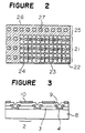
- Figure 2 is a plan view illustrating the patterns of light shielding layers and color filters in the vicinity of the boundary between a display region and a peripheral region in a further example of applying the present invention to a color LCD device where thick-film light shielding layers and thick-film color filters are arranged on the inner surface of its cell.
- color filters 23 are disposed in pixel portions 22, and also light shielding layers 24 are disposed between pixels.
- light shielding layers 26 similar to those between the pixels in the display region, and also color filters 27 which are similar to those in the pixel portions of the display region and have an area corresponding to 5 to 50% of the area of the color filters 23 in the display region.
- the pattern of the color filters 23 is larger than the pattern of openings in the light shielding layers 24 so that the pixel portions 22 in the display region are sufficiently covered with the color filters 23, whereby the peripheries of the color filters 21 overlap the light shielding layers between the pixels. Consequently, in the display region, some overlaps are formed with regard to the color filters 23 and the light shielding layers 24.
- the present invention there are formed, on the entire surface of the peripheral region 25 outside of the display region, light shielding layers 26 similar to those between the pixels in the display region, and also color filters 27 which are similar to those in the pixel portions of the display region and have an area corresponding to 5 to 50% of the area of the aforementoined color filters 23 in the display region.
- the area of the color filters 27 overlapped with the light shielding layers in the peripheral region is reduced to 5 to 50% of the area of the color filters 23 in the pixel portions of the display region, whereby the above disadvantage is diminished and therefore control of the gap uniformity can be facilitated when a cell is produced with spacers disposed on the inner surface of the cell.
- the color filters in the peripheral region may be so arranged as to have the same pattern in a condition where the pixels are arrayed similarly in the peripheral region as well.
- the mask, printing plate or the like used for the color filters in the display region can be utilized also for those in the peripheral region, hence ensuring enhanced productivity.
- the pixels in the peripheral region may be arrayed with the same pitch as that of the pixels in the display region on condition that the pixel arrangement in the peripheral region is the same as in the display region.
- the color filters may be formed with a pitch wider than that of the pixels in the display region.
- the present invention is applied to an STN type LCD device where extremely strict control of the inter-substrate gap uniformity is requisite and monochromatic display can be effected without using any color filter.
- the substrates constituting a liquid crystal cell may be optically isotropic ones and are composed usually of transparent glass, plastic or like material.
- Electrodes are formed on such substrates, and a voltage is selectively applied between desired electrodes to drive the liquid crystal for display.
- the electrodes are composed usually of transparent material such as ITO (In 2 O 3 -SnO 2 ), SnO 2 or the like, and low-resistance leads of Al, Cr or Ti may be combined therewith in accordance with the individual requirements. And a desired patterning process is executed.
- a typical one is a dot matrix LCD device where a multiplicity of row and column electrode groups are existent. For example, striped 1920 electrodes are formed on one substrate while striped 400 electrodes are formed orthogonally thereto on another substrate, whereby a display capacity of 1920 x 400 dots is obtained.
- electrodes are to be disposed in the peripheral region also, for example, striped 2040 electrodes are formed on one substrate while striped 440 electrodes are formed on another substrate to provide 2040 x 440 dots.
- any of the known rubbing, oblique evaporation and other methods may be utilized for aligning the liquid crystal molecules.
- the aligning treatment may be executed after the electrodes are coated with a film of inorganic material such as SiO 2 , TiO 2 or Al 2 O 3 and/or a film of organic material such as polyimide or polyamide in conformity with the individual requirements.
- any suitable ones of the known LCD elements may be employed for the spacer, sealing material, polarizing plate, reflecting plate, illumination means, driving circuit and so forth.
- the color LCD device of the present invention is adapted for use in personal computers, word processors and work stations as well as in any of various color display apparatus as such as liquid crystal television receivers, fish finders, radars, oscilloscopes and dot matrix display units.
- color filters and light shielding layers partially overlap each other in both the display region and the peripheral region, so that when a cell is produced with spacers disposed on its inner surface, the inter-substrate gap can be maintained substantially uniform in each of the display and peripheral regions, hence attaining satisfactory uniformity in the gap between the substrates throughout the cell.
- the light shielding layers alone are disposed in the peripheral region, there are formed, in the display region, some portions which are partially higher than the peripheral region due to the mutual overlaps of the color filters and the light shielding layers, so that the inter-substrate gap in the display region becomes wider than that in the peripheral region to eventually form portions where the inter-substrate gap is gradually varied in the vicinity of the boundary between the display region and the peripheral region, whereby nonuniformity of the background color is prone to occur.
- the display region is also furnished with color filters and light shielding layers which are similar to those in the display region or have some adequate dimensions within a predetermined range.
- mutual overlaps of the color filters and the light shielding layers having substantially the same area as in the display region are formed also in the peripheral region, so that when spacers are disposed, the inter-substrate gap in the peripheral region is rendered substantially uniform and equal to that in the display region.
- the inter-substrate gap can be controlled with a higher accuracy by the provision of electrodes in the peripheral region as well. Consequently there are formed, in the peripheral region also, mutual overlaps of the color filters, the light shielding layers and the electrodes having substantially the same area as that in the display region, so that any variation caused in the inter-substrate gap with disposal of spacers is suppressed in the vicinity of the boundary between the peripheral region and the display region, whereby the inter-substrate gap is rendered substantially uniform even in the outermost portion of the display region to eventually avert nonuniformity of the background color.
- thin-film light shielding layers of chromium were formed to a thickness of 100 nm on a glass substrate, and thick-film color filters (1056 x 272 dots ) were formed by R-G-B three color dyeing process to a thickness of 2.0 ⁇ m on electrode portions corresponding to pixels, in such a manner that the peripheries of the color filters were overlapped with the light shielding layers. And further an overcoat film (leveling layer) of polyimide was formed thereon.
- the surface leveling was executed by forming the overcoat film of polyimide on the color filters and the light shielding layers, but is was difficuit to attain complete flatness of the surface.
- fine irregularities on the color filters were mostly leveled due to the existence of such overcoat film, and some large irregularities resulting from mutual overlaps of the color filters and the light shielding layers in the peripheries of the pixels were considerably eliminated in comparison with the conventional example using none of such overcoat film.
- striped 240 row electrodes were formed on another glass substrate orthogonally to the column electrodes, and an insulator film of SiO 2 -TiO 2 was formed to a thickness of 300 nm on the entire surface. Then, a layer of polyimide was deposited thereon to a thickness of 70 nm or so, and a rubbing process was executed to form an aligning film, thereby constituting a row-electrode substrate in such a manner that liquid crystal molecules have a twist angle of 240° at the time of completion of a cell by combining the row-electrode substrate with the aforementioned column-electrode substrate.
- striped electrodes similar to those in the display region were formed also in the peripheral region surrounding the display region.
- the column-electrode substrate and the row-electrode substrate were so arranged that the twist angle of liquid crystal molecules become 240°, and a cell was constituted by sealing up the peripheries of the substrates. And a dot matrix LC cell was produced with supply of nematic liquid crystal material therein.
- a layer of polyimide was deposited to a thickness of 70 nm on a glass substrate, and it was processed by rubbing to form an aligning film. Two of such substrates were so arranged that liquid crystal molecules have a twist angle of 240° in the reverse direction with respect to the dot matrix LC cell and, after sealing at the peripheries, nematic liquid crystal material was poured therein to produce an LC cell for retardation compensation.
- the dot matrix LC cell was superposed on such retardation compensating LC cell to constitute a laminated structure, and a pair of polarizing plates were disposed on the two sides thereof to manufacture a negative type LCD device.
- the LCD device of such constitution is modified into a positive display type with adequate adjustment of the relationship among the birefringence anisotropy ( ⁇ n) of the liquid crystal material, the aligning direction and the axis of polarization thereof, since any region other than the pixel portion is covered with the light shielding layer, it is still usable as a negative type LCD device when driven by the application of a voltage to desired segments to be darkened, in a manner contrary to driving the ordinary negative type LCD device.
- this LCD device is usable apparently for negative type display regardless of whether it is produced as a negative type or positive type structurally.
- Example 2 In a conventional LCD device having the same constitution as that of Example 1 with the exception that no color filter was provided on any light shielding layer in the peripheral region, the contrast was reduced in the shape of a frame with a width of about 5 mm inside the edge of the display region, and the display quality was deteriorated.
- Modified color LCD devices were manufactured by changing the area of the color filters on the light shielding layer in the peripheral region of Example 1 to 80% (in Example 2) and 60% (in Example 3), respectively.
- Example 2 the inter-substrate gap was substantially uniform in both the display region and the peripheral region, and visually satisfactory color display was attained. However, in Example 3, the uniformity of the inter-substrate gap was slightly lower than that in Examples 1 or 2.
- Light shielding layers having a thickness of about 1.2 ⁇ m were formed by a dyeing process in place of the light shielding layers used in Example 1, and also color filters having a thickness of about 1.8 ⁇ m were formed by a dyeing process.
- Light shielding layers similar to those used in Reference Example 1 were formed on the entire surface of the peripheral region as illustrated in Figure 2, and also color filters similar to those in Reference Example 1 were formed partially (in the area corresponding to about 15% of the color filters in the display region).
- the inter-substrate gap was substantially uniform in both the display region and the peripheral region to consequently realize visually satisfactory display.
- a glass substrate was coated with ITO and then patterned as illustrated in Figure 1 to form striped 960 column electrodes, and an insulator film of SiO 2 -TiO 2 was formed to a thickness of 300 nm on the entire surface.
- Further thin-film light shielding layers of chromium were fromed thereon to a thickness of 100 nm, and thereafter color filters were formed by R-G-B three color dyeing process to a thickness of 2.0 ⁇ m.
- a layer of polyimide was deposited thereon to a thickness of 70 nm or so, and it was processed by rubbing to form an aligning layer, thereby constituting a column-electrode substrate.
- striped 240 row electrodes were formed on another glass substrate orthogonally to the column electrodes, and an insulator film of SiO 2 -TiO 2 was formed to a thickness of 300 nm on the entire surface. Then a layer of polyimide was deposited thereon to a thicknessof 70 nm or so, and a rubbing process was executed to form an aligning film, thereby constituting a row-electrode substrate in such a manner that liquid crystal molecules have a twist angle of 240° at the time of completion of a cell by combining the row-electrode substrate with the aforementioned column-electrode substrate.
- Such row-electrode substrate and column-electrode substrate were assembled as in the foregoing examples to produce a dot matrix LC cell. Subsequently an LC cell for retardation compensation was superposed thereon as in Example 1, and a pair of polarizing plates were disposed on the two sides to manufacture a negative type LCD device.
- the inter-substrate gap was rendered more uniform than that in Comparative Example 1.
- the surface irregularities became greater than those in Example 1 due to the structure where the color filters and the light shielding layers were disposed on the electrodes, so that the uniformity of the inter-substrate gap was slightly inferior to that in Example 1.
- Thin-film light shielding layers of chromium were formed to a thickness of 100 nm on a glass substrate, and thick-film color filters were formed by R-G-B three color dyeing process to a thickness of 2.0 ⁇ m on electrode portions corresponding to pixels, in such a manner that the peripheries of the color filters were overlapped with the light shielding layers. And further an overcoat film (leveling layer) of transparent acrylic resin was formed thereon.
- the surface leveling was thus executed by forming such overcoat film of transparent acrylic resin on the color filters and the light shielding layers, but it was difficult to attain complete flatness of the surface.
- fine irregularities on the color filters were mostly leveled due to the existence of such overcoat film, and some large irregularities resulting from mutual overlaps of the color filters and the light shielding layers in the peripheries of the pixels were eliminated considerably in comparison with the conventional example using none of such overcoat film.
- striped 1056 column electrodes were formed on another glass substrate orthogonally to the row electrodes, and an insulator film of SiO 2 -TiO 2 was formed to a thickness of 50 nm on the entire surface. Then a layer of polyimide was deposited thereon to a thickness of 70 nm or so, and a rubbing process was executed to form an aligning film, thereby constituting a column-electrode substrate in such a manner that liquid crystal molecules have a twist angle of 240° at the time of completion of a cell by combining the column-electrode substrate with the aforementioned row-electrode substrate.
- the row-electrode substrate and the column-electrode substrate were so arranged that the twist angle of liquid crystal molecules became 240°, and a cell was constituted by sealing up the peripheries of the substrates. And a dot matrix LC cell was produced with supply of nematic liquid crystal material therein.
- a layer of polyimide was deposited to a thickness of 70 nm on a glass substrate, and it was processed by rubbing to form and aligning film Two of such substrates were so arranged that liquid crystal molecules have a twist angle of 240° in the reverse direction with respect to the dot matrix LC cell and, after sealing at the peripheries, nematic liquid crystal material was poured therein to produce an LC cell for retardation compensation.
- the dot matrix LC cell was superposed on such retardation compensating LC cell to constitute a laminated structure, and a pair of polarizing plates were disposed on the two sides thereof to manufacture a negative type LCD device.
- Electrodes of ITO equal in pitch to striped 1056 column electrodes for color filters were electrodeposited on a glass substrate, and R-G-B three color filters having a thickness of 2.0 ⁇ m were formed by electrodeposition. And light shielding layers equal in thickness thereto were formed by printing in the space between the color filters.
- An overcoat film of transparent acrylic resin was formed on the color filters, and further it was coated with ITO to a thickness of 240 nm and then patterned to form striped 272 row electrode groups. Subsequently a layer of polyimide was deposited to a thickness of 70 nm or so, and a rubbing process was executed to form an aligning film thereby constituting a row-electrode substrate.
- striped 1056 column electrode groups were formed on another glass substrate orthogonally to the aforementioned row electrode groups, and an insulator film of SiO 2 -TiO 2 was formed on the entire surface to a thickness of 50 nm.
- a layer of polyimide was deposited thereon to a thickness of 70 nm or so, and a rubbing process was executed to form an aligning film, thereby constituting a column-electrode substrate in such as manner that liquid crystal molecules have a twist angle of 240° at the time of completion of a cell of combining the column-electrode substrate with the aforesaid row-electrode substrate.
- the row-electrode substrate and the column-electrode substrate were combined with each other to manufacture an LCD device as in Reference Example 2.
- the device thus assembled had a capability of display with 960 x 240 dots.
- both the display region and the peripheral region are furnished with the color filters, light shielding layers and electrodes having the same pattern (same area) respectively, so that the inter-substrate gap in the display region becomes substantially uniform to consequently attain visually satisfactory color display.
- a glass substrate was coated with ITO and then patterned to form striped 240 row electrode groups and thick-film light shielding layers were formed to a thickness of 1.2 ⁇ m by a dyeing process. Subsequently R-G-B three color filters having a thickness of 2.0 ⁇ m were formed by a dyeing method. Then, a layer of polyimide was deposited thereon to a thickness of 70 nm or so, and a rubbing process was executed to form an aligning layer, thereby constituting a column-electrode substrate.
- striped 960 column electrode groups were formed on another glass substrate in a manner to be orthogonal to the row electrode groups, and an insulator film of SiO 2 -TiO 2 was formed to a thickness of 50 nm on the entire surface. Then a layer of polyimide was deposited thereon to a thickness of 70 nm or so, and a rubbing process was executed to form an aligning film, thereby constituting a row-electrode substrate in such a manner that liquid crytal molecules have a twist angle of 240° at the time of completion of a cell by combining the column-electrode substrate with the aforementioned row-electrode substrate.
- Such row-electrode substrate and column-electrode substrate were assembled as in Reference Example 2 to produce a dot matrix LC cell. Subsequently an LC cell for retardation compensation was superposed thereon as in Example 2, and a pair of polarizing plates were disposed on the two sides to manufacture a negative type LCD device having a display capacity of 912 x 208 dots.
- an optical compensating sheet composed of a uniaxial polymer film of polycarbonate was superposed on each of the two surfaces of the dot matrix LC cell to manufacture an LCD device.
- Such LCD device was connected to a driving circuit and then was driven in the same manner as Examples 1 to 7.
- the resultant effects attained were similar to those in the foregoing examples.
- Such LCD device was connected to a driving circuit and then was driven in the same manner as Examples 1-7.
- the resultant effects attained were similar to those in Examples 1-7.
- the gap between the substrates can be maintained uniform with facility to eventually realize visually satisfactory color display.
- color-filters for both the display region and the peripheral region can be produced by using the same mask or printing plate, hence realizing high productivity.
- any variation in the inter-substrate gap is suppressed in the vicinity of the boundary between the peripheral region and the display region, whereby such inter-substrate gap is retained substantially uniform even at the outermost periphery of the display region, hence averting nonuniformity of the background color.
Landscapes
- Physics & Mathematics (AREA)
- Nonlinear Science (AREA)
- Mathematical Physics (AREA)
- Chemical & Material Sciences (AREA)
- Crystallography & Structural Chemistry (AREA)
- General Physics & Mathematics (AREA)
- Optics & Photonics (AREA)
- Liquid Crystal (AREA)
Claims (10)
- Farb-Flüssigkristallanzeige-Vorrichtung mit einem Anzeigebereich (1;21) und einem den Anzeigebereich (1;21) umgebenden Umfangsbereich (5;15), wobei der Anzeigebereich (1;21) Lichtabschirmungsschichten (4;24) und Farbfilter (3;23) auf der Innenflache einer Zelle aufweist, und mit einander gegenüberstehenden Gruppen von Elektroden (10) zum Vornehmend der Anzeige, dadurch gekennzeichnet, dass(a) die Anzeigevorrichtung eine vom Punktmatrixtyp ist, wobei die Farbfilter (3;23) in Pixel-Abschnitten ausgebildet sind;(b) die Anzeigevorrichtung eine vom STN-Typ ist, die zur schwarzen und weißen Anzeige in der Lage ist;(c) die Lichtabschirmungsschichten (6;26) im Anzeigebereich (1;21) in wechselseitiger teilweiser Überlappung mit den Pixel-Abschnitten der Farbfilter (3;23) angeordnet sind, wahrend(d1) Lichtabschirmungsschichten (6;26) über der gesamten Oberfläche des Umfangsbereiches (5;25) angeordnet sind und(d2) Farbfilter (7;27) ähnlich denen des Anzeigebereiches (1;21) auch im Umfangsbereich (1;21) angeordnet sind.
- Vorrichtung nach Anspruch 1, worin der Anzeigebereich einer vom Punktmatrixtyp ist, wobei streifenförmige Elektrodengruppen einander gegenüberstehen, um einzelne Pixel zu bilden, und sie Farbfilter von mindestens zwei Farben aufweist, und die benachbarten Pixel unterschiedlicher Farben als ein Satz zum Vornehmen der Anzeige dienen.
- Vorrichtung nach Anspruch 2, worin die Lichtabschirmungsschichten aus dünnen Filmen zusammengesetzt sind, während die Farbfilter aus dicken Filmen zusammengesetzt sind, wobei die Farbfilter eine Fläche aufweisen, die 50 bis 100% der Fläche der Farbfilter im Anzeigebereich entspricht.
- Vorrichtung nach Anspruch 1, worin sowohl die Lichtabschirmungsschichten als auch die Farbfilter aus Dickfilmen bestehen.
- Vorrichtung nach Anspruch 2, worin sowohl die Lichtabschirmungsschichten als auch die Farbfilter aus Dickfilmen bestehen, wobei die Farbfilter eine Fläche aufweisen, die 5 bis 50% der Fläche der Farbfilter im Anzeigebereich entspricht.
- Vorrichtung nach einem der Ansprüche 1 bis 4, worin die in dem Umfangsbereich benutzten Substrate mit Elektroden ähnlich denen im Anzeigebreich versehen sind.
- Vorrichtung nach Anspruch 1, worin deren Flüssigkristallschicht einen Verdrillungswinkel von 160° bis 300° aufweist, und ein Verzögerungskompensator der Flüssigkristallschicht überlagert ist, um die von dieser Schicht herrührende elliptische Polarisation zu kompensieren.
- Vorrichtung nach Anspruch 7, worin der Verzögerungskompensator aus einer Flüssigkristallschicht besteht.
- Vorrichtung nach Anspruch 7, worin der Verzögerungskompensator aus einem Verzögerungsfilm besteht.
- Verfahren zur Anwendung der Farb-Flüssigkristallanzeige-Vorrichtung nach den Ansprüchen 1 bis 9, bei dem auf der rückwärtigen Seite der Vorrichtung ein Hinterlicht geschaffen wird, um die Funktion der Vorrichtung als ein Negativtyp zu ermöglichen.
Applications Claiming Priority (6)
| Application Number | Priority Date | Filing Date | Title |
|---|---|---|---|
| JP96856/88 | 1988-04-21 | ||
| JP9685688 | 1988-04-21 | ||
| JP63096856A JP2901063B2 (ja) | 1988-04-21 | 1988-04-21 | カラー液晶表示素子 |
| JP274462/88 | 1988-11-01 | ||
| JP27446288 | 1988-11-01 | ||
| JP63274462A JPH02123325A (ja) | 1988-11-01 | 1988-11-01 | カラー液晶表示装置 |
Publications (4)
| Publication Number | Publication Date |
|---|---|
| EP0338412A2 EP0338412A2 (de) | 1989-10-25 |
| EP0338412A3 EP0338412A3 (de) | 1991-01-02 |
| EP0338412B1 EP0338412B1 (de) | 1995-03-29 |
| EP0338412B2 true EP0338412B2 (de) | 2000-05-10 |
Family
ID=26438017
Family Applications (1)
| Application Number | Title | Priority Date | Filing Date |
|---|---|---|---|
| EP19890106561 Expired - Lifetime EP0338412B2 (de) | 1988-04-21 | 1989-04-13 | Farbflüssigkristall-Anzeigevorrichtung und ihr Ansteuerungsverfahren |
Country Status (2)
| Country | Link |
|---|---|
| EP (1) | EP0338412B2 (de) |
| DE (1) | DE68921910T3 (de) |
Cited By (1)
| Publication number | Priority date | Publication date | Assignee | Title |
|---|---|---|---|---|
| CN1320377C (zh) * | 2001-06-25 | 2007-06-06 | 精工爱普生株式会社 | 滤色器、基板、电光装置、电子仪器、成膜方法和装置 |
Families Citing this family (12)
| Publication number | Priority date | Publication date | Assignee | Title |
|---|---|---|---|---|
| US5420708A (en) * | 1990-08-31 | 1995-05-30 | Idemitsu Kosan Co., Ltd. | Color filters, including taking out electrodes or post-ito layer |
| JPH04120511A (ja) * | 1990-09-11 | 1992-04-21 | Sharp Corp | 液晶表示装置 |
| JPH04269713A (ja) | 1991-02-25 | 1992-09-25 | Seiko Instr Inc | 多色パターンの製造方法 |
| JPH0540258A (ja) * | 1991-08-06 | 1993-02-19 | Nippon Paint Co Ltd | 多色表示装置の製造方法 |
| EP1703317B1 (de) * | 1992-02-27 | 2008-08-06 | Canon Kabushiki Kaisha | Flüssigkristallanzeigevorrichtung |
| GB9211282D0 (en) * | 1992-05-28 | 1992-07-15 | Philips Electronics Uk Ltd | Liquid crystal display devices |
| JPH08122767A (ja) * | 1994-10-28 | 1996-05-17 | Nec Kagoshima Ltd | カラー液晶ディスプレイ |
| US5936694A (en) * | 1995-04-26 | 1999-08-10 | Canon Kabushiki Kaisha | Liquid crystal device and process for producing same |
| JPH09138390A (ja) * | 1995-09-14 | 1997-05-27 | Canon Inc | 液晶表示装置 |
| US6348959B1 (en) * | 1998-12-21 | 2002-02-19 | Philips Electronics North America Corporation | Reflective LCD with dark borders |
| CN111338119B (zh) * | 2018-12-19 | 2023-01-03 | 上海仪电显示材料有限公司 | 彩色滤光基板及色度测量方法 |
| CN114035362B (zh) | 2021-11-15 | 2023-10-13 | 惠州华星光电显示有限公司 | 液晶显示面板与显示装置 |
Family Cites Families (3)
| Publication number | Priority date | Publication date | Assignee | Title |
|---|---|---|---|---|
| FR2595155B1 (fr) * | 1986-02-28 | 1988-04-29 | Commissariat Energie Atomique | Procede de realisation de filtres colores en bandes et d'electrodes en bandes auto-alignes pour une cellule d'affichage polychrome a film liquide et cellule correspondante |
| JPS62269928A (ja) * | 1986-05-19 | 1987-11-24 | Toppan Printing Co Ltd | カラ−フイルタ− |
| DE3752219T2 (de) * | 1986-05-19 | 1999-02-18 | Seiko Epson Corp., Tokio/Tokyo | Flüssigkristall-Anzeigevorrichtung |
-
1989
- 1989-04-13 EP EP19890106561 patent/EP0338412B2/de not_active Expired - Lifetime
- 1989-04-13 DE DE1989621910 patent/DE68921910T3/de not_active Expired - Lifetime
Cited By (1)
| Publication number | Priority date | Publication date | Assignee | Title |
|---|---|---|---|---|
| CN1320377C (zh) * | 2001-06-25 | 2007-06-06 | 精工爱普生株式会社 | 滤色器、基板、电光装置、电子仪器、成膜方法和装置 |
Also Published As
| Publication number | Publication date |
|---|---|
| DE68921910T3 (de) | 2000-08-17 |
| EP0338412B1 (de) | 1995-03-29 |
| EP0338412A3 (de) | 1991-01-02 |
| DE68921910D1 (de) | 1995-05-04 |
| DE68921910T2 (de) | 1995-12-14 |
| EP0338412A2 (de) | 1989-10-25 |
Similar Documents
| Publication | Publication Date | Title |
|---|---|---|
| US5617230A (en) | Color liquid crystal display device with peripheral pixels in a light-shielded state | |
| KR100269196B1 (ko) | 액정표시장치 | |
| EP0715202B1 (de) | Anzeigevorrichtung | |
| US7209198B2 (en) | Color filter array substrate and fabricating method thereof | |
| US6515727B2 (en) | Color LCD device | |
| EP0338412B2 (de) | Farbflüssigkristall-Anzeigevorrichtung und ihr Ansteuerungsverfahren | |
| JP3242114B2 (ja) | カラー液晶表示装置 | |
| EP0707232B1 (de) | Flüssigkristall-Farbanzeigetafel | |
| US20100302482A1 (en) | Color filter substrate, liquid crystal display panel, liquid crystal display device, and production method of color filter substrate | |
| JPWO1997006463A1 (ja) | カラー液晶表示装置 | |
| JPH1048640A (ja) | アクティブマトリクス型液晶表示装置 | |
| KR20040107048A (ko) | 액정표시장치 및 이의 제조 방법 | |
| US20060103789A1 (en) | Liquid crystal display panel and liquid crystal display device | |
| KR20040081387A (ko) | 액정 표시 장치 및 전자 기기 | |
| JP2901063B2 (ja) | カラー液晶表示素子 | |
| JP3536447B2 (ja) | カラー液晶表示素子 | |
| JP2005215115A (ja) | 液晶表示装置 | |
| JPH11271757A (ja) | カラー液晶表示素子及びその製造方法 | |
| JPH02123325A (ja) | カラー液晶表示装置 | |
| JPH1152351A (ja) | 液晶表示装置 | |
| KR20020091454A (ko) | 액정표시장치 | |
| JP2003121833A (ja) | カラー液晶表示装置 | |
| JPH10160917A (ja) | 液晶表示装置 | |
| JPH06265877A (ja) | 液晶表示素子 | |
| JPH07287220A (ja) | 液晶装置およびその製造方法 |
Legal Events
| Date | Code | Title | Description |
|---|---|---|---|
| PUAI | Public reference made under article 153(3) epc to a published international application that has entered the european phase |
Free format text: ORIGINAL CODE: 0009012 |
|
| AK | Designated contracting states |
Kind code of ref document: A2 Designated state(s): CH DE FR GB LI NL |
|
| PUAL | Search report despatched |
Free format text: ORIGINAL CODE: 0009013 |
|
| AK | Designated contracting states |
Kind code of ref document: A3 Designated state(s): CH DE FR GB LI NL |
|
| 17P | Request for examination filed |
Effective date: 19901221 |
|
| 17Q | First examination report despatched |
Effective date: 19921126 |
|
| GRAA | (expected) grant |
Free format text: ORIGINAL CODE: 0009210 |
|
| AK | Designated contracting states |
Kind code of ref document: B1 Designated state(s): CH DE FR GB LI NL |
|
| PG25 | Lapsed in a contracting state [announced via postgrant information from national office to epo] |
Ref country code: CH Effective date: 19950329 Ref country code: LI Effective date: 19950329 Ref country code: FR Free format text: LAPSE BECAUSE OF NON-PAYMENT OF DUE FEES Effective date: 19950329 Ref country code: NL Free format text: LAPSE BECAUSE OF FAILURE TO SUBMIT A TRANSLATION OF THE DESCRIPTION OR TO PAY THE FEE WITHIN THE PRESCRIBED TIME-LIMIT Effective date: 19950329 |
|
| REF | Corresponds to: |
Ref document number: 68921910 Country of ref document: DE Date of ref document: 19950504 |
|
| ET | Fr: translation filed | ||
| REG | Reference to a national code |
Ref country code: CH Ref legal event code: PL |
|
| NLV1 | Nl: lapsed or annulled due to failure to fulfill the requirements of art. 29p and 29m of the patents act | ||
| PLAV | Examination of admissibility of opposition |
Free format text: ORIGINAL CODE: EPIDOS OPEX |
|
| PLBQ | Unpublished change to opponent data |
Free format text: ORIGINAL CODE: EPIDOS OPPO |
|
| PLBI | Opposition filed |
Free format text: ORIGINAL CODE: 0009260 |
|
| PLAV | Examination of admissibility of opposition |
Free format text: ORIGINAL CODE: EPIDOS OPEX |
|
| 26 | Opposition filed |
Opponent name: CANON KABUSHIKI KAISHA Effective date: 19951229 |
|
| PLBF | Reply of patent proprietor to notice(s) of opposition |
Free format text: ORIGINAL CODE: EPIDOS OBSO |
|
| PLBF | Reply of patent proprietor to notice(s) of opposition |
Free format text: ORIGINAL CODE: EPIDOS OBSO |
|
| PLBF | Reply of patent proprietor to notice(s) of opposition |
Free format text: ORIGINAL CODE: EPIDOS OBSO |
|
| RDAH | Patent revoked |
Free format text: ORIGINAL CODE: EPIDOS REVO |
|
| APAC | Appeal dossier modified |
Free format text: ORIGINAL CODE: EPIDOS NOAPO |
|
| APAE | Appeal reference modified |
Free format text: ORIGINAL CODE: EPIDOS REFNO |
|
| PGFP | Annual fee paid to national office [announced via postgrant information from national office to epo] |
Ref country code: FR Payment date: 19980409 Year of fee payment: 10 |
|
| APAC | Appeal dossier modified |
Free format text: ORIGINAL CODE: EPIDOS NOAPO |
|
| APAC | Appeal dossier modified |
Free format text: ORIGINAL CODE: EPIDOS NOAPO |
|
| PLAW | Interlocutory decision in opposition |
Free format text: ORIGINAL CODE: EPIDOS IDOP |
|
| REG | Reference to a national code |
Ref country code: FR Ref legal event code: ST |
|
| PUAH | Patent maintained in amended form |
Free format text: ORIGINAL CODE: 0009272 |
|
| STAA | Information on the status of an ep patent application or granted ep patent |
Free format text: STATUS: PATENT MAINTAINED AS AMENDED |
|
| 27A | Patent maintained in amended form |
Effective date: 20000510 |
|
| AK | Designated contracting states |
Kind code of ref document: B2 Designated state(s): CH DE FR GB LI NL |
|
| EN | Fr: translation not filed | ||
| REG | Reference to a national code |
Ref country code: GB Ref legal event code: IF02 |
|
| APAH | Appeal reference modified |
Free format text: ORIGINAL CODE: EPIDOSCREFNO |
|
| REG | Reference to a national code |
Ref country code: GB Ref legal event code: 732E |
|
| PGFP | Annual fee paid to national office [announced via postgrant information from national office to epo] |
Ref country code: DE Payment date: 20080417 Year of fee payment: 20 |
|
| PGFP | Annual fee paid to national office [announced via postgrant information from national office to epo] |
Ref country code: GB Payment date: 20080416 Year of fee payment: 20 |
|
| REG | Reference to a national code |
Ref country code: GB Ref legal event code: PE20 Expiry date: 20090412 |
|
| PG25 | Lapsed in a contracting state [announced via postgrant information from national office to epo] |
Ref country code: GB Free format text: LAPSE BECAUSE OF EXPIRATION OF PROTECTION Effective date: 20090412 |