EP0337540A1 - Combination of a support and a semiconductor body and method of manufacturing such a combination - Google Patents
Combination of a support and a semiconductor body and method of manufacturing such a combination Download PDFInfo
- Publication number
- EP0337540A1 EP0337540A1 EP89200844A EP89200844A EP0337540A1 EP 0337540 A1 EP0337540 A1 EP 0337540A1 EP 89200844 A EP89200844 A EP 89200844A EP 89200844 A EP89200844 A EP 89200844A EP 0337540 A1 EP0337540 A1 EP 0337540A1
- Authority
- EP
- European Patent Office
- Prior art keywords
- support
- semiconductor body
- metal layer
- combination
- projection
- Prior art date
- Legal status (The legal status is an assumption and is not a legal conclusion. Google has not performed a legal analysis and makes no representation as to the accuracy of the status listed.)
- Granted
Links
Images
Classifications
-
- H—ELECTRICITY
- H01—ELECTRIC ELEMENTS
- H01L—SEMICONDUCTOR DEVICES NOT COVERED BY CLASS H10
- H01L24/00—Arrangements for connecting or disconnecting semiconductor or solid-state bodies; Methods or apparatus related thereto
- H01L24/80—Methods for connecting semiconductor or other solid state bodies using means for bonding being attached to, or being formed on, the surface to be connected
- H01L24/83—Methods for connecting semiconductor or other solid state bodies using means for bonding being attached to, or being formed on, the surface to be connected using a layer connector
-
- G—PHYSICS
- G01—MEASURING; TESTING
- G01L—MEASURING FORCE, STRESS, TORQUE, WORK, MECHANICAL POWER, MECHANICAL EFFICIENCY, OR FLUID PRESSURE
- G01L9/00—Measuring steady of quasi-steady pressure of fluid or fluent solid material by electric or magnetic pressure-sensitive elements; Transmitting or indicating the displacement of mechanical pressure-sensitive elements, used to measure the steady or quasi-steady pressure of a fluid or fluent solid material, by electric or magnetic means
- G01L9/0041—Transmitting or indicating the displacement of flexible diaphragms
- G01L9/0042—Constructional details associated with semiconductive diaphragm sensors, e.g. etching, or constructional details of non-semiconductive diaphragms
-
- H—ELECTRICITY
- H01—ELECTRIC ELEMENTS
- H01L—SEMICONDUCTOR DEVICES NOT COVERED BY CLASS H10
- H01L24/00—Arrangements for connecting or disconnecting semiconductor or solid-state bodies; Methods or apparatus related thereto
- H01L24/01—Means for bonding being attached to, or being formed on, the surface to be connected, e.g. chip-to-package, die-attach, "first-level" interconnects; Manufacturing methods related thereto
- H01L24/26—Layer connectors, e.g. plate connectors, solder or adhesive layers; Manufacturing methods related thereto
-
- H—ELECTRICITY
- H01—ELECTRIC ELEMENTS
- H01L—SEMICONDUCTOR DEVICES NOT COVERED BY CLASS H10
- H01L24/00—Arrangements for connecting or disconnecting semiconductor or solid-state bodies; Methods or apparatus related thereto
- H01L24/80—Methods for connecting semiconductor or other solid state bodies using means for bonding being attached to, or being formed on, the surface to be connected
- H01L24/81—Methods for connecting semiconductor or other solid state bodies using means for bonding being attached to, or being formed on, the surface to be connected using a bump connector
-
- H—ELECTRICITY
- H01—ELECTRIC ELEMENTS
- H01L—SEMICONDUCTOR DEVICES NOT COVERED BY CLASS H10
- H01L2224/00—Indexing scheme for arrangements for connecting or disconnecting semiconductor or solid-state bodies and methods related thereto as covered by H01L24/00
- H01L2224/80—Methods for connecting semiconductor or other solid state bodies using means for bonding being attached to, or being formed on, the surface to be connected
- H01L2224/81—Methods for connecting semiconductor or other solid state bodies using means for bonding being attached to, or being formed on, the surface to be connected using a bump connector
- H01L2224/8119—Arrangement of the bump connectors prior to mounting
- H01L2224/81191—Arrangement of the bump connectors prior to mounting wherein the bump connectors are disposed only on the semiconductor or solid-state body
-
- H—ELECTRICITY
- H01—ELECTRIC ELEMENTS
- H01L—SEMICONDUCTOR DEVICES NOT COVERED BY CLASS H10
- H01L2224/00—Indexing scheme for arrangements for connecting or disconnecting semiconductor or solid-state bodies and methods related thereto as covered by H01L24/00
- H01L2224/80—Methods for connecting semiconductor or other solid state bodies using means for bonding being attached to, or being formed on, the surface to be connected
- H01L2224/81—Methods for connecting semiconductor or other solid state bodies using means for bonding being attached to, or being formed on, the surface to be connected using a bump connector
- H01L2224/818—Bonding techniques
- H01L2224/81801—Soldering or alloying
-
- H—ELECTRICITY
- H01—ELECTRIC ELEMENTS
- H01L—SEMICONDUCTOR DEVICES NOT COVERED BY CLASS H10
- H01L2224/00—Indexing scheme for arrangements for connecting or disconnecting semiconductor or solid-state bodies and methods related thereto as covered by H01L24/00
- H01L2224/80—Methods for connecting semiconductor or other solid state bodies using means for bonding being attached to, or being formed on, the surface to be connected
- H01L2224/83—Methods for connecting semiconductor or other solid state bodies using means for bonding being attached to, or being formed on, the surface to be connected using a layer connector
- H01L2224/8319—Arrangement of the layer connectors prior to mounting
-
- H—ELECTRICITY
- H01—ELECTRIC ELEMENTS
- H01L—SEMICONDUCTOR DEVICES NOT COVERED BY CLASS H10
- H01L2224/00—Indexing scheme for arrangements for connecting or disconnecting semiconductor or solid-state bodies and methods related thereto as covered by H01L24/00
- H01L2224/80—Methods for connecting semiconductor or other solid state bodies using means for bonding being attached to, or being formed on, the surface to be connected
- H01L2224/83—Methods for connecting semiconductor or other solid state bodies using means for bonding being attached to, or being formed on, the surface to be connected using a layer connector
- H01L2224/838—Bonding techniques
- H01L2224/8385—Bonding techniques using a polymer adhesive, e.g. an adhesive based on silicone, epoxy, polyimide, polyester
-
- H—ELECTRICITY
- H01—ELECTRIC ELEMENTS
- H01L—SEMICONDUCTOR DEVICES NOT COVERED BY CLASS H10
- H01L2924/00—Indexing scheme for arrangements or methods for connecting or disconnecting semiconductor or solid-state bodies as covered by H01L24/00
- H01L2924/01—Chemical elements
- H01L2924/01013—Aluminum [Al]
-
- H—ELECTRICITY
- H01—ELECTRIC ELEMENTS
- H01L—SEMICONDUCTOR DEVICES NOT COVERED BY CLASS H10
- H01L2924/00—Indexing scheme for arrangements or methods for connecting or disconnecting semiconductor or solid-state bodies as covered by H01L24/00
- H01L2924/01—Chemical elements
- H01L2924/01014—Silicon [Si]
-
- H—ELECTRICITY
- H01—ELECTRIC ELEMENTS
- H01L—SEMICONDUCTOR DEVICES NOT COVERED BY CLASS H10
- H01L2924/00—Indexing scheme for arrangements or methods for connecting or disconnecting semiconductor or solid-state bodies as covered by H01L24/00
- H01L2924/01—Chemical elements
- H01L2924/01033—Arsenic [As]
-
- H—ELECTRICITY
- H01—ELECTRIC ELEMENTS
- H01L—SEMICONDUCTOR DEVICES NOT COVERED BY CLASS H10
- H01L2924/00—Indexing scheme for arrangements or methods for connecting or disconnecting semiconductor or solid-state bodies as covered by H01L24/00
- H01L2924/06—Polymers
- H01L2924/078—Adhesive characteristics other than chemical
- H01L2924/07802—Adhesive characteristics other than chemical not being an ohmic electrical conductor
-
- H—ELECTRICITY
- H01—ELECTRIC ELEMENTS
- H01L—SEMICONDUCTOR DEVICES NOT COVERED BY CLASS H10
- H01L2924/00—Indexing scheme for arrangements or methods for connecting or disconnecting semiconductor or solid-state bodies as covered by H01L24/00
- H01L2924/15—Details of package parts other than the semiconductor or other solid state devices to be connected
- H01L2924/151—Die mounting substrate
- H01L2924/1515—Shape
- H01L2924/15151—Shape the die mounting substrate comprising an aperture, e.g. for underfilling, outgassing, window type wire connections
-
- Y—GENERAL TAGGING OF NEW TECHNOLOGICAL DEVELOPMENTS; GENERAL TAGGING OF CROSS-SECTIONAL TECHNOLOGIES SPANNING OVER SEVERAL SECTIONS OF THE IPC; TECHNICAL SUBJECTS COVERED BY FORMER USPC CROSS-REFERENCE ART COLLECTIONS [XRACs] AND DIGESTS
- Y10—TECHNICAL SUBJECTS COVERED BY FORMER USPC
- Y10T—TECHNICAL SUBJECTS COVERED BY FORMER US CLASSIFICATION
- Y10T29/00—Metal working
- Y10T29/49—Method of mechanical manufacture
- Y10T29/49002—Electrical device making
- Y10T29/49117—Conductor or circuit manufacturing
- Y10T29/49124—On flat or curved insulated base, e.g., printed circuit, etc.
- Y10T29/4913—Assembling to base an electrical component, e.g., capacitor, etc.
- Y10T29/49139—Assembling to base an electrical component, e.g., capacitor, etc. by inserting component lead or terminal into base aperture
- Y10T29/4914—Assembling to base an electrical component, e.g., capacitor, etc. by inserting component lead or terminal into base aperture with deforming of lead or terminal
-
- Y—GENERAL TAGGING OF NEW TECHNOLOGICAL DEVELOPMENTS; GENERAL TAGGING OF CROSS-SECTIONAL TECHNOLOGIES SPANNING OVER SEVERAL SECTIONS OF THE IPC; TECHNICAL SUBJECTS COVERED BY FORMER USPC CROSS-REFERENCE ART COLLECTIONS [XRACs] AND DIGESTS
- Y10—TECHNICAL SUBJECTS COVERED BY FORMER USPC
- Y10T—TECHNICAL SUBJECTS COVERED BY FORMER US CLASSIFICATION
- Y10T29/00—Metal working
- Y10T29/49—Method of mechanical manufacture
- Y10T29/49002—Electrical device making
- Y10T29/49117—Conductor or circuit manufacturing
- Y10T29/49124—On flat or curved insulated base, e.g., printed circuit, etc.
- Y10T29/49147—Assembling terminal to base
- Y10T29/49151—Assembling terminal to base by deforming or shaping
- Y10T29/49153—Assembling terminal to base by deforming or shaping with shaping or forcing terminal into base aperture
Definitions
- the invention relates to a combination of a support and a semiconductor body, in which a deformable metal layer is disposed between the semiconductor body and the support and the semiconductor body is connected to the support by pressing the semiconductor body and the support against each other other under pressure after heating the metal layer.
- Such a combination of a semiconductor body and a support is known from Netherlands Patent Application 7415668.
- the metal layer is enclosed between two parallel extending boundary surfaces of the support and the semiconductor body.
- connection is satisfactory, but in certain cases it may be desirable to realize a more rigid connection between the support and the semiconductor body.
- the semiconductor body is provided at its surface facing the support with at least one projecting part, which is embedded in the metal layer.
- the projection then has a closed contour, by means of this projection a particularly satisfactory vacuum-tight connection can further be obtained between the semiconductor body and the support, which may be important, for example, in pressure sensors and the like.
- a further aspect of the invention relates to a method of connecting a semiconductor body to a support, in which a deformable metal layer is provided between the semiconductor body and the support and the semiconductor body is connected to the support by pressing the semiconductor body and the support against each other under pressure at an elevated temperature.
- a projecting part integral with the semiconductor body is formed on the semiconductor body on the side to face the support and this projecting part is pressed into the metal layer when providing the semiconductor.
- a semiconductor body to be manufactured in a simple manner can be secured very firmly to a support.
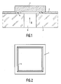
- a semiconductor body 1 is provided on a support 3 with the interposition of a metal layer 2.
- the insulating support 3 may be made, for example, of glass.
- the metal layer 2 will consist of aluminium and will generally have a thickness of the order of 10 ⁇ m.
- the semiconductor body 1 is provided on its side facing the support 3 with a projection, which is constituted in the embodiment shown by a continuous projecting edge 4 having a cross-section of triangular form.
- the height of this projection projecting beyond the boundary surface of the semiconductor body is about half the thickness of the metal layer 2 in the non-deformed state.
- the projection 4 can be formed in a simple and efficacious manner by removing parts of the starting material located around the projection by etching.
- the metal layer 2 is arranged between the support and the semiconductor body 1, after which, whilst heating the metal layer 2, the semiconductor body 1 and the support 3 are pressed towards each other, the continuous projection 4 penetrating in the manner shown in Figure 1 into the metal layer.
- the metal layer 2 may be applied to the support 3, for example by vapour deposition.
- the projection 4 it is not necessary for the projection 4 to have a closed contour, while it is also possible that several projections located at a certain relative distance are provided.
- a projection having a closed contour is particularly advantageous, however, if the projection, as is the case in the embodiment shown in Figure 2, surrounds a recess 5 provided in the support 3 and different pressures prevail on either side of the support. In fact it has been found that by the use of a projection having a closed contour a particularly satisfactory gas-tight connection can be obtained between the support and the semiconductor body.
- the form of the cross-section of the projection 4 may also be different from the triangular form shown; for example, viewed in cross-section the projection may have the form of a truncated cone.
- the projection is provided with an aluminium coating so that, when the semiconductor body is contacted with the metal layer consisting of aluminium, a connection of aluminium on aluminium is obtained.
- the projection may then also be provided with a silicon oxide layer, on which the aluminium coating is formed.
Abstract
Description
- The invention relates to a combination of a support and a semiconductor body, in which a deformable metal layer is disposed between the semiconductor body and the support and the semiconductor body is connected to the support by pressing the semiconductor body and the support against each other other under pressure after heating the metal layer.
- Such a combination of a semiconductor body and a support is known from Netherlands Patent Application 7415668. In this known combination, the metal layer is enclosed between two parallel extending boundary surfaces of the support and the semiconductor body.
- In general, such a connection is satisfactory, but in certain cases it may be desirable to realize a more rigid connection between the support and the semiconductor body.
- According to the invention, this can be achieved in that the semiconductor body is provided at its surface facing the support with at least one projecting part, which is embedded in the metal layer.
- In practice it has been found that by the use of one or several projecting parts engaging into the metal layer provided between the support and the semiconductor a considerable improvement of the adhesion between the semiconductor body and the support is obtained.
- If the projection then has a closed contour, by means of this projection a particularly satisfactory vacuum-tight connection can further be obtained between the semiconductor body and the support, which may be important, for example, in pressure sensors and the like.
- A further aspect of the invention relates to a method of connecting a semiconductor body to a support, in which a deformable metal layer is provided between the semiconductor body and the support and the semiconductor body is connected to the support by pressing the semiconductor body and the support against each other under pressure at an elevated temperature.
- According to the invention, before the semiconductor body is provided on the support, a projecting part integral with the semiconductor body is formed on the semiconductor body on the side to face the support and this projecting part is pressed into the metal layer when providing the semiconductor.
- By the use of the method according to the invention, a semiconductor body to be manufactured in a simple manner can be secured very firmly to a support.
- The invention will now be described more fully with reference to an embodiment of the combination according to the invention shown in the accompanying Figures.
- Figure 1 shows in sectional view a combination of a support and a semiconductor body provided thereon with the interposition of a metal layer;
- Figure 2 is an elevation of the semiconductor body taken on the arrow II in Figure 1.
- As shown diagrammatically in Figure 1, a
semiconductor body 1 is provided on asupport 3 with the interposition of ametal layer 2. - The
insulating support 3 may be made, for example, of glass. - Preferably, the
metal layer 2 will consist of aluminium and will generally have a thickness of the order of 10 µm. - As will further appear from Figures 1 and 2, the
semiconductor body 1 is provided on its side facing thesupport 3 with a projection, which is constituted in the embodiment shown by a continuous projectingedge 4 having a cross-section of triangular form. The height of this projection projecting beyond the boundary surface of the semiconductor body is about half the thickness of themetal layer 2 in the non-deformed state. - The
projection 4 can be formed in a simple and efficacious manner by removing parts of the starting material located around the projection by etching. - Before the connection between the
support 3 and thesemiconductor body 1 is established, themetal layer 2 is arranged between the support and thesemiconductor body 1, after which, whilst heating themetal layer 2, thesemiconductor body 1 and thesupport 3 are pressed towards each other, thecontinuous projection 4 penetrating in the manner shown in Figure 1 into the metal layer. Themetal layer 2 may be applied to thesupport 3, for example by vapour deposition. - It has been found that the adhesion between the semiconductor body and the metal layer is considerably more satisfactory than in the embodiment in which the boundary surface of the semiconductor body facing the
support 3 is flat. - As a matter of course, variations of and or additions to the embodiment of the construction according to the invention described above are conceivable within the scope of the invention.
- For example, it is not necessary for the
projection 4 to have a closed contour, while it is also possible that several projections located at a certain relative distance are provided. A projection having a closed contour is particularly advantageous, however, if the projection, as is the case in the embodiment shown in Figure 2, surrounds arecess 5 provided in thesupport 3 and different pressures prevail on either side of the support. In fact it has been found that by the use of a projection having a closed contour a particularly satisfactory gas-tight connection can be obtained between the support and the semiconductor body. - The form of the cross-section of the
projection 4 may also be different from the triangular form shown; for example, viewed in cross-section the projection may have the form of a truncated cone. - Another possibility consists in that, before the semiconductor body is arranged on the support, the projection is provided with an aluminium coating so that, when the semiconductor body is contacted with the metal layer consisting of aluminium, a connection of aluminium on aluminium is obtained. The projection may then also be provided with a silicon oxide layer, on which the aluminium coating is formed.
Claims (7)
Applications Claiming Priority (2)
| Application Number | Priority Date | Filing Date | Title |
|---|---|---|---|
| NL8800901A NL8800901A (en) | 1988-04-08 | 1988-04-08 | COMBINATION OF A CARRIER AND A SEMICONDUCTOR BODY AND METHOD FOR PRODUCING SUCH COMBINATION. |
| NL8800901 | 1988-04-08 |
Publications (2)
| Publication Number | Publication Date |
|---|---|
| EP0337540A1 true EP0337540A1 (en) | 1989-10-18 |
| EP0337540B1 EP0337540B1 (en) | 1994-10-12 |
Family
ID=19852089
Family Applications (1)
| Application Number | Title | Priority Date | Filing Date |
|---|---|---|---|
| EP89200844A Expired - Lifetime EP0337540B1 (en) | 1988-04-08 | 1989-04-03 | Combination of a support and a semiconductor body and method of manufacturing such a combination |
Country Status (5)
| Country | Link |
|---|---|
| US (2) | US4929999A (en) |
| EP (1) | EP0337540B1 (en) |
| JP (1) | JPH01310545A (en) |
| DE (1) | DE68918741T2 (en) |
| NL (1) | NL8800901A (en) |
Families Citing this family (13)
| Publication number | Priority date | Publication date | Assignee | Title |
|---|---|---|---|---|
| JPH0770806B2 (en) * | 1990-08-22 | 1995-07-31 | 株式会社エーユーイー研究所 | Electronic circuit by ultrasonic welding and manufacturing method thereof |
| US5585282A (en) * | 1991-06-04 | 1996-12-17 | Micron Technology, Inc. | Process for forming a raised portion on a projecting contact for electrical testing of a semiconductor |
| US5385869A (en) * | 1993-07-22 | 1995-01-31 | Motorola, Inc. | Semiconductor chip bonded to a substrate and method of making |
| US5478779A (en) * | 1994-03-07 | 1995-12-26 | Micron Technology, Inc. | Electrically conductive projections and semiconductor processing method of forming same |
| US5326428A (en) | 1993-09-03 | 1994-07-05 | Micron Semiconductor, Inc. | Method for testing semiconductor circuitry for operability and method of forming apparatus for testing semiconductor circuitry for operability |
| DE4409068C2 (en) * | 1994-03-14 | 1998-05-28 | Hartmann & Braun Ag | Bonding process and bond connection produced therewith |
| DE4433689C2 (en) * | 1994-09-21 | 1996-07-11 | Siemens Ag | Chip configuration and use of a corresponding chip |
| FR2738395B1 (en) * | 1995-08-31 | 1997-10-10 | Commissariat Energie Atomique | SELF-SUPPORTING DEVICE FOR THE PROPAGATION OF MICROWAVE WAVES AND METHODS OF MAKING SUCH A DEVICE |
| JPH10270496A (en) | 1997-03-27 | 1998-10-09 | Hitachi Ltd | Electronic device, information processor, semiconductor device, semiconductor chip, and mounting method thereof |
| FR2775810B1 (en) * | 1998-03-09 | 2000-04-28 | Gemplus Card Int | NON-CONTACT CARD MANUFACTURING PROCESS |
| US6078103A (en) * | 1998-10-29 | 2000-06-20 | Mcdonnell Douglas Corporation | Dimpled contacts for metal-to-semiconductor connections, and methods for fabricating same |
| JP4159778B2 (en) * | 2001-12-27 | 2008-10-01 | 三菱電機株式会社 | IC package, optical transmitter and optical receiver |
| US9076674B2 (en) * | 2012-09-25 | 2015-07-07 | Intermolecular, Inc. | Method and apparatus for improving particle performance |
Citations (4)
| Publication number | Priority date | Publication date | Assignee | Title |
|---|---|---|---|---|
| US3888708A (en) * | 1972-02-17 | 1975-06-10 | Kensall D Wise | Method for forming regions of predetermined thickness in silicon |
| FR2293704A1 (en) * | 1974-12-02 | 1976-07-02 | Philips Nv | PRESSURE INDICATOR |
| US4125820A (en) * | 1975-10-06 | 1978-11-14 | Honeywell Inc. | Stress sensor apparatus |
| EP0142692A1 (en) * | 1983-10-12 | 1985-05-29 | Siemens Aktiengesellschaft | Mounting of semiconductor components on a circuit board |
Family Cites Families (20)
| Publication number | Priority date | Publication date | Assignee | Title |
|---|---|---|---|---|
| DE45437C (en) * | J. ROGGY in Saarlouis | Security money box | ||
| US2352640A (en) * | 1942-11-03 | 1944-07-04 | Fed Telephone & Radio Corp | Plate rectifier |
| US3363308A (en) * | 1962-07-30 | 1968-01-16 | Texas Instruments Inc | Diode contact arrangement |
| US3422320A (en) * | 1965-12-23 | 1969-01-14 | Gen Motors Corp | Sealing technique for composite ferrous-copper base alloy capsules for semiconductor devices |
| US3492545A (en) * | 1968-03-18 | 1970-01-27 | Westinghouse Electric Corp | Electrically and thermally conductive malleable layer embodying lead foil |
| US3611064A (en) * | 1969-07-14 | 1971-10-05 | Gen Electric | Ohmic contact to n-type silicon carbide, comprising nickel-titanium-gold |
| GB1297046A (en) * | 1969-08-25 | 1972-11-22 | ||
| JPS538872B2 (en) * | 1971-10-23 | 1978-04-01 | ||
| GB1426874A (en) * | 1972-05-03 | 1976-03-03 | Mullard Ltd | Method of sealing electrical component envelopes |
| US4024627A (en) * | 1974-04-29 | 1977-05-24 | Amp Incorporated | Package mounting of electronic chips, such as light emitting diodes |
| JPS53119693A (en) * | 1977-03-29 | 1978-10-19 | Toshiba Corp | Semiconductor pressure transducer |
| US4185378A (en) * | 1978-02-10 | 1980-01-29 | Chuo Meiban Mfg. Co., LTD. | Method for attaching component leads to printed circuit base boards and printed circuit base board advantageously used for working said method |
| US4754316A (en) * | 1982-06-03 | 1988-06-28 | Texas Instruments Incorporated | Solid state interconnection system for three dimensional integrated circuit structures |
| JPS599976A (en) * | 1982-07-09 | 1984-01-19 | Toshiba Corp | Absolute pressure type semiconductor pressure sensor |
| US4753601A (en) * | 1983-10-14 | 1988-06-28 | Amp Incorporated | Circuit board thickness compensator |
| US4640438A (en) * | 1986-03-17 | 1987-02-03 | Comienco Limited | Cover for semiconductor device packages |
| GB2194477A (en) * | 1986-08-28 | 1988-03-09 | Stc Plc | Solder joint |
| DE3788263T2 (en) * | 1986-09-25 | 1994-03-24 | Toshiba Kawasaki Kk | Method for electrically connecting two objects. |
| JPH07101747B2 (en) * | 1987-03-05 | 1995-11-01 | 日本電装株式会社 | Semiconductor pressure sensor |
| US4970624A (en) * | 1990-01-22 | 1990-11-13 | Molex Incorporated | Electronic device employing a conductive adhesive |
-
1988
- 1988-04-08 NL NL8800901A patent/NL8800901A/en not_active Application Discontinuation
-
1989
- 1989-04-03 DE DE68918741T patent/DE68918741T2/en not_active Expired - Fee Related
- 1989-04-03 EP EP89200844A patent/EP0337540B1/en not_active Expired - Lifetime
- 1989-04-04 US US07/334,063 patent/US4929999A/en not_active Expired - Lifetime
- 1989-04-05 JP JP1084914A patent/JPH01310545A/en active Pending
-
1990
- 1990-01-23 US US07/468,679 patent/US5057458A/en not_active Expired - Fee Related
Patent Citations (4)
| Publication number | Priority date | Publication date | Assignee | Title |
|---|---|---|---|---|
| US3888708A (en) * | 1972-02-17 | 1975-06-10 | Kensall D Wise | Method for forming regions of predetermined thickness in silicon |
| FR2293704A1 (en) * | 1974-12-02 | 1976-07-02 | Philips Nv | PRESSURE INDICATOR |
| US4125820A (en) * | 1975-10-06 | 1978-11-14 | Honeywell Inc. | Stress sensor apparatus |
| EP0142692A1 (en) * | 1983-10-12 | 1985-05-29 | Siemens Aktiengesellschaft | Mounting of semiconductor components on a circuit board |
Non-Patent Citations (1)
| Title |
|---|
| ELECTRONIC COMPONENTS AND APPLICATIONS, vol. 6, no. 3, 1984, pages 149-154; G. KEITEL: "The KP100A monolithic pressure sensor" * |
Also Published As
| Publication number | Publication date |
|---|---|
| US4929999A (en) | 1990-05-29 |
| JPH01310545A (en) | 1989-12-14 |
| DE68918741D1 (en) | 1994-11-17 |
| NL8800901A (en) | 1989-11-01 |
| EP0337540B1 (en) | 1994-10-12 |
| DE68918741T2 (en) | 1995-04-27 |
| US5057458A (en) | 1991-10-15 |
Similar Documents
| Publication | Publication Date | Title |
|---|---|---|
| EP0337540A1 (en) | Combination of a support and a semiconductor body and method of manufacturing such a combination | |
| US4761518A (en) | Ceramic-glass-metal packaging for electronic components incorporating unique leadframe designs | |
| US6083578A (en) | Design improvements to vacuum glazing | |
| AU4949200A (en) | Solid electrolytic capacitor and method of manufacture thereof | |
| US4278195A (en) | Method for low temperature bonding of silicon and silicon on sapphire and spinel to nickel and nickel steel and apparatus using such _a bonding technique | |
| CA2184161A1 (en) | Robust bond for micromachined sensor | |
| US20020062552A1 (en) | Multilayered ceramic substrate and production method therefor | |
| CA1058878A (en) | Ceramic to metal seal | |
| CA1063732A (en) | Semiconductor device with pressure electrical contacts having irregular surfaces | |
| KR970076948A (en) | Sheathed end seals for vacuum breakers | |
| EP3645821B1 (en) | Use of a gasket and sealing system for a vig unit production | |
| US4795866A (en) | Vacuum tube switch which uses low temperature solder | |
| JPH06105787B2 (en) | High pressure resistant pressure sensor | |
| EP0341964A3 (en) | Silicon micro sensor and manufacturing method therefor | |
| US4290080A (en) | Method of making a strain buffer for a semiconductor device | |
| US20040246551A1 (en) | Window | |
| JPH06181276A (en) | Lead for semiconductor device | |
| CA2143641A1 (en) | Process for producing miniature components | |
| US6756138B1 (en) | Micro-electromechanical devices | |
| US5417584A (en) | Flat cable/connector strain relief connection and method thereof | |
| US4249668A (en) | Envelope for camera tube | |
| JPH10508805A (en) | Method of manufacturing a layer structure on a substrate | |
| WO1997003784A2 (en) | Component assembly | |
| EP0670667A1 (en) | Direct copper bonded substrates | |
| EP0498713B1 (en) | Process of mounting miniature electronic components with solderable leads on a flexible substrate |
Legal Events
| Date | Code | Title | Description |
|---|---|---|---|
| PUAI | Public reference made under article 153(3) epc to a published international application that has entered the european phase |
Free format text: ORIGINAL CODE: 0009012 |
|
| AK | Designated contracting states |
Kind code of ref document: A1 Designated state(s): DE FR GB |
|
| 17P | Request for examination filed |
Effective date: 19900417 |
|
| 17Q | First examination report despatched |
Effective date: 19920409 |
|
| GRAA | (expected) grant |
Free format text: ORIGINAL CODE: 0009210 |
|
| AK | Designated contracting states |
Kind code of ref document: B1 Designated state(s): DE FR GB |
|
| REF | Corresponds to: |
Ref document number: 68918741 Country of ref document: DE Date of ref document: 19941117 |
|
| ET | Fr: translation filed | ||
| REG | Reference to a national code |
Ref country code: FR Ref legal event code: CD |
|
| PLBE | No opposition filed within time limit |
Free format text: ORIGINAL CODE: 0009261 |
|
| STAA | Information on the status of an ep patent application or granted ep patent |
Free format text: STATUS: NO OPPOSITION FILED WITHIN TIME LIMIT |
|
| 26N | No opposition filed | ||
| PGFP | Annual fee paid to national office [announced via postgrant information from national office to epo] |
Ref country code: GB Payment date: 19970401 Year of fee payment: 9 |
|
| PGFP | Annual fee paid to national office [announced via postgrant information from national office to epo] |
Ref country code: FR Payment date: 19970422 Year of fee payment: 9 |
|
| PGFP | Annual fee paid to national office [announced via postgrant information from national office to epo] |
Ref country code: DE Payment date: 19970624 Year of fee payment: 9 |
|
| PG25 | Lapsed in a contracting state [announced via postgrant information from national office to epo] |
Ref country code: GB Free format text: LAPSE BECAUSE OF NON-PAYMENT OF DUE FEES Effective date: 19980403 |
|
| PG25 | Lapsed in a contracting state [announced via postgrant information from national office to epo] |
Ref country code: FR Free format text: THE PATENT HAS BEEN ANNULLED BY A DECISION OF A NATIONAL AUTHORITY Effective date: 19980430 |
|
| GBPC | Gb: european patent ceased through non-payment of renewal fee |
Effective date: 19980403 |
|
| PG25 | Lapsed in a contracting state [announced via postgrant information from national office to epo] |
Ref country code: DE Free format text: LAPSE BECAUSE OF NON-PAYMENT OF DUE FEES Effective date: 19990202 |
|
| REG | Reference to a national code |
Ref country code: FR Ref legal event code: ST |