EP0332313A2 - Wärmesenken-Zusammenbau für Halbleiter - Google Patents
Wärmesenken-Zusammenbau für Halbleiter Download PDFInfo
- Publication number
- EP0332313A2 EP0332313A2 EP89301617A EP89301617A EP0332313A2 EP 0332313 A2 EP0332313 A2 EP 0332313A2 EP 89301617 A EP89301617 A EP 89301617A EP 89301617 A EP89301617 A EP 89301617A EP 0332313 A2 EP0332313 A2 EP 0332313A2
- Authority
- EP
- European Patent Office
- Prior art keywords
- heat sink
- semiconductor device
- resin
- base
- blocks
- Prior art date
- Legal status (The legal status is an assumption and is not a legal conclusion. Google has not performed a legal analysis and makes no representation as to the accuracy of the status listed.)
- Withdrawn
Links
Images
Classifications
-
- H—ELECTRICITY
- H10—SEMICONDUCTOR DEVICES; ELECTRIC SOLID-STATE DEVICES NOT OTHERWISE PROVIDED FOR
- H10W—GENERIC PACKAGES, INTERCONNECTIONS, CONNECTORS OR OTHER CONSTRUCTIONAL DETAILS OF DEVICES COVERED BY CLASS H10
- H10W40/00—Arrangements for thermal protection or thermal control
- H10W40/60—Securing means for detachable heating or cooling arrangements, e.g. clamps
Definitions
- This invention relates to heat sink assemblies for semiconductor devices.
- semiconductor devices have been provided with heat sinks, to dissipate thermal energy produced by the devices in use, and thereby reduce the risk of damage to the devices, due to overheating.
- Typical heat sink and/or connector arrangements for high power semiconductor devices comprise an assembly of various parts, which are usually connected together by nuts, bolts, etc.
- Such assemblies have a high metal content, to provide satisfactory heat sinks, and it will be appreciated that such metal parts will have an appreciable coefficient of thermal expansion, which is certainly much different to that of the semiconductor device itself.
- problems can arise of potential mechanical damage to the semiconductor device, as the metal parts move with changes in temperature.
- Considerable design work is usually entailed, to meet the design problems.
- the present invention aims to provide a semiconductor heat sink assembly of generally improved and relatively simple design.
- a semiconductor heat sink assembly comprising a heat sink base, a semiconductor device, and a heat sink clamping block, the clamping block being secured to the base by means of a cured resin of good electrical resistance and good thermal conductivity, in such a position as to bear against one face of the semiconductor thereby to clamp it in a desired position.
- heat sink clamping blocks as aforesaid, each secured to the base by said resin to bear against opposite faces of the semiconductor device, and thereby clamp the device between said blocks.
- said base defines a channel within which the or each said block is secured.
- the channel is preferably open ended, either at one or both ends.
- the invention provides a method of securing a semiconductor device to a heat sink, comprising the steps of positioning a heat sink clamping block on a heat sink base with a resin of good electrical resistance and good thermal conductivity disposed between said block and base, and allowing the resin to cure so as to secure said block in said base in such a position as to bear against one face of the semiconductor device to clamp it in a desired position.
- two bases as aforesaid are disposed in said heat sink base with said resin between said blocks and said base, and the resin is allowed to cure with said blocks in such a position as to bear against opposite faces of the semiconductor device and thereby clamp the semiconductor device between said blocks. It is further preferred that the or each block is clamped in its desired position by clamping means, during setting of the resin.
- the resin is allowed to cure with the or each said block bearing against a spacer, the or each said block is forced away from its clamping position after setting of the resin, the spacer is thereafter removed, and the semiconductor device is inserted in place of the spacer.
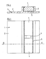
- the illustrated heat sink assembly comprises a heat sink base 1 which is formed as an extrusion of a metal of good thermal conductivity (e.g. aluminium).
- the base has a substantially flat mounting/heat dissipation area 2, and a generally C-shaped channel 3, which is open at both ends.
- Disposed within the channel 3 are a pair of heat sink blocks 4, which are also extruded of metal of good thermal conductivity, and are secured within the channel 3 by means of a thin layer of resin 5, which is interposed between the blocks 4 and the channel 3, thereby to isolate the blocks from the channel.
- the resin 5 is preferably of high electrical resistivity and high thermal conductivity (for example, of at least 4 Kw/m°C).
- the heat sink blocks 4 are so secured in the channel 3 by means of the resin 5, as to clamp therebetween a semiconductor device 6, opposing faces of which are borne against by contacting faces of the heat sink blocks 4.
- the blocks 4 make good electrical and thermal contact with the semiconductor device 6. Therefore, the blocks 4 may serve not only to conduct heat away from the semiconductor device 6, but also to afford reliable electrical connectors therefor. To this end, the blocks 4 may be formed or provided with suitable means for affording external electrical connections.
- Heat that is transferred to the blocks 4 from the semiconductor device 6 is subsequently dissipated into the heat sink base, via the resin layer 5.
- the surface area of the resin layer 5 is substantial, whereas its thickness is relatively small (e.g. 2 mm). Thus, any relative thermal impedance presented by the resin layer may be kept to a minimum.
- the resin preferably has a relatively high thermal conductivity, this may typically be significantly less than that of the thermal conductivity of the metal base 2 and blocks 4.
- the layer of resin 5 serves to mount the blocks 4 securely within the channel 3 of the base 2, whilst retaining a significant clamping force against the opposite faces of the semiconductor device 6.
- the heat sink base 2 and blocks 4 will tend to expand.
- the characteristics of this layer e.g. thickness, components of resin, filler size, catalyst,etc
- the semiconductor device 6 is placed in the channel 3 of the heat sink base 2.
- the two blocks 4 are then engaged within the channel 3, and brought to bear against the opposite faces of the semiconductor device 6 where they are then held in place by external clamps. Resin is applied between the blocks 4 and the inner walls of the channel 3, and this may be applied either before insertion of the blocks, or after.
- the resin is then allowed to cure, whilst the external clamps are maintained in place. Upon full curing of the resin, the clamps are released, and the semiconductor device is then clamped in place between the blocks 4, due to the securing of the blocks 4 within the channel 3, by means of the resin.
- the layer of resin 5 may permit a small amount of relative movement between the blocks 4. As indicated above, the characteristics of the resin 5 will determine how much variation in clamping force may be expected, upon removing the clamping means.
- a spacer is initially disposed between the two blocks 4, which are again held in position by external clamps, until the resin 5 has fully cured. At this point, the two blocks 4 are spaced apart, the spacer is removed, the semiconductor device 6 is inserted between the blocks 4, and the blocks 4 are released, to clamp the semiconductor device firmly in position.
- the illustrated apparatus and above described methods afford a means for readily clamping a semiconductor device in a heat sink assembly, whilst at the same time affording simple and reliable connections to the opposing faces of the semiconductor device.
Landscapes
- Cooling Or The Like Of Semiconductors Or Solid State Devices (AREA)
Applications Claiming Priority (2)
| Application Number | Priority Date | Filing Date | Title |
|---|---|---|---|
| GB8803991A GB2215127A (en) | 1988-02-20 | 1988-02-20 | Semiconductor heat sink assembly |
| GB8803991 | 1988-02-20 |
Publications (2)
| Publication Number | Publication Date |
|---|---|
| EP0332313A2 true EP0332313A2 (de) | 1989-09-13 |
| EP0332313A3 EP0332313A3 (de) | 1990-09-05 |
Family
ID=10632079
Family Applications (1)
| Application Number | Title | Priority Date | Filing Date |
|---|---|---|---|
| EP19890301617 Withdrawn EP0332313A3 (de) | 1988-02-20 | 1989-02-20 | Wärmesenken-Zusammenbau für Halbleiter |
Country Status (2)
| Country | Link |
|---|---|
| EP (1) | EP0332313A3 (de) |
| GB (1) | GB2215127A (de) |
Family Cites Families (3)
| Publication number | Priority date | Publication date | Assignee | Title |
|---|---|---|---|---|
| GB1486745A (en) * | 1976-07-28 | 1977-09-21 | Aei Semiconductors Ltd | Mounting assemblies for electronic components |
| US4092697A (en) * | 1976-12-06 | 1978-05-30 | International Business Machines Corporation | Heat transfer mechanism for integrated circuit package |
| US4564885A (en) * | 1984-09-10 | 1986-01-14 | General Instrument Corporation | Rectifier with slug construction and mold for fabricating same |
-
1988
- 1988-02-20 GB GB8803991A patent/GB2215127A/en not_active Withdrawn
-
1989
- 1989-02-20 EP EP19890301617 patent/EP0332313A3/de not_active Withdrawn
Also Published As
| Publication number | Publication date |
|---|---|
| EP0332313A3 (de) | 1990-09-05 |
| GB2215127A (en) | 1989-09-13 |
| GB8803991D0 (en) | 1988-03-23 |
Similar Documents
| Publication | Publication Date | Title |
|---|---|---|
| US4899255A (en) | Heat sink clip and assembly and method of manufacture | |
| US5920249A (en) | Protective method of support for an electromagnetic apparatus | |
| CA2097097C (en) | Heat sink mounting system for semiconductor devices | |
| CA2396652A1 (en) | Method and apparatus for electrically heating a screed assembly in a paving machine | |
| US9530750B2 (en) | Method of clamping a semiconductor assembly | |
| KR20100110346A (ko) | 히트싱크 및 히트싱크 형성 방법 | |
| JP2018522408A (ja) | 車両バッテリのための仮圧縮性圧縮リミッタを備える熱電モジュール | |
| US5168425A (en) | Mounting arrangements for high voltage/high power semiconductors | |
| EP0332313A2 (de) | Wärmesenken-Zusammenbau für Halbleiter | |
| GB2201123A (en) | Electrical conductor | |
| US20240113397A1 (en) | Busbar assembly, vehicle battery, and method for producing a busbar assembly | |
| US4040085A (en) | Power semiconductor assembly and the method and apparatus for assembly thereof | |
| JP2002355835A (ja) | 熱伝導性基板の製造方法 | |
| CN217388147U (zh) | 一种线缆固定装置 | |
| US3946353A (en) | Mounting system for infrared tubes | |
| US5417584A (en) | Flat cable/connector strain relief connection and method thereof | |
| CN119426911B (zh) | 一种新能源汽车电机铝端盖的生产设备及生产方法 | |
| CN215903352U (zh) | 一种用于电动汽车热管的固化成型夹具 | |
| SU848217A1 (ru) | Устройство дл создани давлени пРи диффузиОННОй CBAPKE | |
| CN114345985B (zh) | 一种直线电机校直方法 | |
| US7257001B2 (en) | Device and method for fastener-free connection via a heat-shrinkable insert | |
| JP2979488B2 (ja) | 積層ゴム体の製造装置 | |
| EP0913841A1 (de) | Trägermechanismus für ein elektromagnetisches Gerät | |
| JP2000294069A (ja) | 樹脂モールド電気機器の製造方法 | |
| JP3289600B2 (ja) | フィルム打ち抜き貼り付け装置およびその組み立て方法 |
Legal Events
| Date | Code | Title | Description |
|---|---|---|---|
| PUAI | Public reference made under article 153(3) epc to a published international application that has entered the european phase |
Free format text: ORIGINAL CODE: 0009012 |
|
| AK | Designated contracting states |
Kind code of ref document: A2 Designated state(s): DE FR IT |
|
| PUAL | Search report despatched |
Free format text: ORIGINAL CODE: 0009013 |
|
| AK | Designated contracting states |
Kind code of ref document: A3 Designated state(s): DE FR IT |
|
| STAA | Information on the status of an ep patent application or granted ep patent |
Free format text: STATUS: THE APPLICATION IS DEEMED TO BE WITHDRAWN |
|
| 18D | Application deemed to be withdrawn |
Effective date: 19910306 |