EP0332297B1 - Asynchroner Zähler mit Preset - Google Patents
Asynchroner Zähler mit Preset Download PDFInfo
- Publication number
- EP0332297B1 EP0332297B1 EP89301340A EP89301340A EP0332297B1 EP 0332297 B1 EP0332297 B1 EP 0332297B1 EP 89301340 A EP89301340 A EP 89301340A EP 89301340 A EP89301340 A EP 89301340A EP 0332297 B1 EP0332297 B1 EP 0332297B1
- Authority
- EP
- European Patent Office
- Prior art keywords
- bit
- flip
- output
- counter
- flop
- Prior art date
- Legal status (The legal status is an assumption and is not a legal conclusion. Google has not performed a legal analysis and makes no representation as to the accuracy of the status listed.)
- Expired - Lifetime
Links
- 230000000295 complement effect Effects 0.000 claims description 13
- 238000003491 array Methods 0.000 claims description 4
- 101000685663 Homo sapiens Sodium/nucleoside cotransporter 1 Proteins 0.000 description 5
- 101000821827 Homo sapiens Sodium/nucleoside cotransporter 2 Proteins 0.000 description 5
- 102100023116 Sodium/nucleoside cotransporter 1 Human genes 0.000 description 5
- 102100021541 Sodium/nucleoside cotransporter 2 Human genes 0.000 description 5
- 230000007704 transition Effects 0.000 description 2
- 238000000034 method Methods 0.000 description 1
- 238000004377 microelectronic Methods 0.000 description 1
Images
Classifications
-
- H—ELECTRICITY
- H03—ELECTRONIC CIRCUITRY
- H03K—PULSE TECHNIQUE
- H03K23/00—Pulse counters comprising counting chains; Frequency dividers comprising counting chains
- H03K23/58—Gating or clocking signals not applied to all stages, i.e. asynchronous counters
-
- H—ELECTRICITY
- H03—ELECTRONIC CIRCUITRY
- H03K—PULSE TECHNIQUE
- H03K23/00—Pulse counters comprising counting chains; Frequency dividers comprising counting chains
- H03K23/64—Pulse counters comprising counting chains; Frequency dividers comprising counting chains with a base or radix other than a power of two
- H03K23/66—Pulse counters comprising counting chains; Frequency dividers comprising counting chains with a base or radix other than a power of two with a variable counting base, e.g. by presetting or by adding or suppressing pulses
- H03K23/665—Pulse counters comprising counting chains; Frequency dividers comprising counting chains with a base or radix other than a power of two with a variable counting base, e.g. by presetting or by adding or suppressing pulses by presetting
Definitions
- the present invention relates to loadable ripple counters.
- Counters count sequential input pulses, providing a parallel output indicating the counted value.
- Ripple counters routinely employ flip-flops configured to alternate their outputs upon each clock pulse.
- An N-bit ripple counter employs N flip-flops connected in a chain so that each flip-flop output both clocks the next flip-flop and is used as a bit of the N-bit parallel output of the counter.
- a ripple counter having this configuration is described in Millman, Microelectronics , (McGraw-Hill 1979), pp. 220-222.
- a divide-by-n counter employing a plurality of sub-circuits each employing a flip-flop and a gate that is inputted with the output of a preceding flip-flop corresponding to a next less significant bit, and a data input providing a divisor value.
- Loadable N-bit ripple counters are configured to be loaded with an N-bit parallel input so that counting begins at the loaded number.
- An example of a common prior art loadable ripple counter is shown in Fig. 1 and described in detail below.
- the invention features a loadable N-bit ripple counter having N bit subcircuits, each employing a flip-flop and a bit loading element.
- the flip-flop is configured to alternate its flip-flop output every time that it receives a clock pulse and has means to control its output to a known state when a flip-flop control signal is asserted.
- the bit loading element is inputted with the flip-flop output and a bit input of a multibit number being loaded into the counter and outputs a bit output of the counter.
- the bit output is controlled by the states of the flip-flop output and the bit input.
- the bit loading element is a gate (most preferably an exclusive-NOR gate); and in some other preferred embodiments, the bit loading element is a multiplexer having two signal inputs connected to receive true and complement flip-flop outputs and a control input that determines whether the true output or the complement output is provided as the multiplexer output.
- the bit output except for the most significant bit, serves as a clock for the next more significant bit subcircuit; the flip-flops are set to known states by clearing them; and the flip-flop output is connected to its D-input to cause its output to alternate state.
- the savings in space may permit use of a smaller die size.
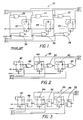
- Fig. 1 labeled prior art, is a schematic of a known loadable three-bit ripple counter.
- Fig. 2 is a schematic of a loadable three-bit ripple counter according to the invention.
- Fig. 3 is a schematic of an alternative embodiment of a loadable three-bit ripple counter according to the invention.
- Fig. 1 is shown common prior art loadable ripple counter 20 that employs NAND gates 28-38 to control the set and clear functions of D-flip-flops 22, 24, 26 to load counter 20 with a three-bit number indicated by the LD0H, LD1H, LD2H, LD0L, LD1L, and LD2L inputs.
- Counter 20 counts INC H pulses provided to flip-flop 22, the least significant bit flip-flop. The complement output of each flip-flop clocks the next flip-flop (except for flip-flop 26), is used as a bit of the three-bit counter output (CN0, CN1, CN2), and is provided to its D input (causing each flip-flop 22, 24, 26 to alternate its output every clock period).
- a counter of this configuration has twelve gates and eight nets, i.e., connections between components, for each output bit when implemented in a gate array using a DEC15GA gate array library.
- ripple counter 40 utilizes clearable D-flip-flops 42, 44, and 46 and exclusive-NOR gates 48, 50, 52.
- Counter 40 counts pulses provided as the INC H input, provides a three-bit parallel output (CNT0, CNT1, CNT2), and is loaded with a three-bit parallel input (LD0H, LD1H, LD2H).
- Flip-flops 42, 44, 46 are connected to be cleared by a flip-flop control signal, LOAD L. The complement output of each flip-flop 42, 44, 46 is connected to its corresponding D input, causing each flip-flop to alternate its output every clock pulse.
- the true output of flip-flop 42 is inputted to exclusive-NOR gate 48, which is also inputted with the least significant bit, LD0H, of the loaded number
- the output of gate 48 is outputted as CNT0 and clocks flip-flop 44.
- the true output of flip-flop 44 is inputted to gate 50, which is also inputted with the second bit, LD1H, of the loaded number.
- the output of gate 50 is outputted as CNT1 and clocks flop-flop 46.
- the true output of flip-flop 46 is inputted to gate 52, which is also inputted with the third bit, LD2H, of the loaded number.
- the output of gate 52 is outputted as CNT2.
- a counter of this configuration utilizes eleven gates and five nets for each output bit when implemented in a gate array using a DEC15GA gate array library.
- ripple counter 60 utilizes clearable D-flip-flops 62, 64, 66 and two-to-one multiplexers 68, 70, 72. Like counter 40, counter 60 counts pulses provided as the INC H input, provides a three-bit parallel output (CNT0, CNT1, CNT2), and is loaded with a three-bit parallel input (LD0H, LD1H, LD2H). Flip-flops 62, 64, 66 are connected to be cleared by a flip-flop control signal, LOAD L. The true outputs of flip-flops 62, 64, and 66 are inputted to the A inputs of multiplexers 68, 70, and 22.
- the complement outputs of flip-flops 62, 64, 66 are inputted to their own D inputs (to provide alternating flip-flop outputs) and are inputted to the B inputs of multiplexers 68, 70, 72, respectively.
- the three-bit parallel inputs, LD0H, LD1H, and LD2H, of the loaded number are inputted to the control inputs, S, of multiplexers 68, 70, and 72, respectively.
- the output of multiplexer 68 is outputted as CNTO and inputted as the clock for flip-flop 64.
- the output of multiplexer 70 is outputted as CNT1 and inputted as the clock for flip-flop 66.
- the output of multiplexer 72 is outputted as CNT2.
- a counter of this configuration utilizes ten gates and six nets for each output bit when implemented as a gate array using a DEC15GA gate array library
- counter 40 is loaded with the loaded number indicated by the gates of LD0H, LD1H, LD2H by asserting the flip-flop control signal, LOAD L.
- This clears the outputs of flip-flops 42, 44, and 46, in turn causing the outputs of gates 48, 50, 52, and thus the three bits of the counter output, CNT0, CNT1, CNT2, to be determined by the gates of LD0H, LD1H and LD2H.
- LOAD L is deasserted
- counter 40 counts INC H pulses. As each INC H pulse is received, the CNTO bit of counter 40 transitions to the logical NOT of its current gate.
- counter 60 is loaded by asserting the flip-flop control signal, LOAD L, which clears the true outputs and sets the complement outputs of flip-flops 62, 64, and 66.
- the counter output which is the output of multiplexers 68, 70, and 72, is now determined by the states of LD0H, LD1H, and LD2H, which are fed to the S multiplexer inputs. If the S input is high, multiplexers 68, 70, and 72 output the true input; if the S input is low, multiplexers 68, 70, 72 output the complement input.
- Loadable ripple counters 40, 60 are advantageous in that they use fewer gates and nets than the prior art, thereby saving space. In integrated circuits employing a plurality of ripple counters according to the invention, the savings in space may permit use of a smaller die size. Ripple counters according to the invention also do not require settable flip-flops but can employ simpler, less-expensive flip-flops.
- the invention is applicable to both up counters, as in Figs. 2 and 3, and to down counters.
Landscapes
- Logic Circuits (AREA)
Claims (9)
- Voreinstellbarer N-Bit Asynchronzähler (40,60), der N Bit-Unterschaltungen umfaßt, wobei jede Unterschaltung einen einzelnen Bit-Ausgang des N-Bit-Zählerausgangs (CHT0-CHT2) aufweist, das Zählerausgangssignal eine Funktion eines voreingestellten binären Worts mit N Bit ist, das auf jeden der 2N Werte einstellbar ist, und jede Bit-Unterschaltung folgendes umfaßt:
ein Flipflop (42-46;62-66), das so konfiguriert ist, um seinen Flipflop-Ausgang zu jeder Zeit zu ändern, zu der es einen Takt empfängt, wobei das Flipflop, das dem niedrigstwertigen Bit zugeordnet ist, einen Takt von außerhalb des Asynchronzählers empfängt, und das Flipflop eine Einrichtung besitzt, um den Flipflop-Ausgang in einen bekannten Zustand zurückzusetzen, wenn ein Flipflop-Steuersignal (LOAD L) aktiviert ist, wobei der bekannte Zustand solange erhalten bleibt, bis das Steuersignal deaktiviert ist; und
ein Bit-Voreinstellungselement (48-52;68-72), das so geschaltet ist, daß es das Flipflop-Ausgangssignal (Q) und ein entsprechendes Bit-Eingangssignal (LD0H-LD2H) des vorher eingestellten N-Bitworts empfängt und ein Bit-Ausgangssignal (CNT0-CNT2) des Zählers ausgibt, wobei das Bit-Ausgangssignal durch die Zustände des Flipflop-Ausgangs und des entsprechenden Bit-Eingangs gesteuert wird und das Bit-Ausgangssignal des Bit-Voreinstellungselements, mit Ausnahme der dem höchstwertigen Bit zugeordneten Unterschaltung, ebenfalls so geschaltet ist, daß es als Takt für eine nächst höherwertige Bit-Unterschaltung dient. - Zähler nach Anspruch 1, bei dem das Bit-Voreinstellungselement (48-52) Verknüpfungsglied aufweist.
- Zähler nach Anspruch 2, bei dem das Bit-Voreinstellungselement (48-52) ein Exklusiv-NOR-Glied umfaßt.
- Zähler nach Anspruch 1, bei dem
das Flipflop (62-66) einen echten Ausgang (Q) und einen komplementären Ausgang (QN) besitzt;
und
das Bit-Voreinstellungselement (68-72) einen Multiplexer aufweist, der zwei Signaleingänge (A,B) besitzt, die so geschaltet sind, daß sie wahre Ausgangssignale (Q) bzw. komplementäre Ausgangssignale (QN) empfangen, und einen Steuereingang (S), der so geschaltet ist, daß er das Bit-Eingangssignal empfängt, wobei der Multiplexer entweder das wahre Ausgangssignal oder das komplementäre Ausgangssignal als sein Ausgangssignal (Z) abhängig vom Zustand seines Bit-Eingangs ausgibt. - Zähler nach Anspruch 1, bei dem die Einrichtung zum Betreiben des Flipflop-Ausgangs eine Einrichtung zum Zurücksetzen des Flipflops umfaßt, wodurch bewirkt wird, daß der Flipflop-Ausgang LOW wird.
- Zähler nach Anspruch 1, bei dem ein komplementärer Ausgang (QN) des Flipflops (48-52;62-66) mit einem D-Eingang des Flipflops verbunden ist, um zu bewirken, daß seine wahren und komplementären Ausgänge (Q,QN) einen alternierenden Zustand annehmen.
- Zähler nach Anspruch 1, bei dem die Flipflops (42-46;62-66) und die Bit-Voreinstellungselemente (48-52;68-72) als Gate Arrays ausgeführt sind.
- Zähler nach Anspruch 3, bei dem die Flipflops (42-46) und die die Bit-Voreinstellungselemente (48-52) als Gate Arrays ausgeführt sind.
- Zähler nach Anspruch 4, bei dem die Flipflops (62-66) und die die Bit-Voreinstellungselemente (68-72) als Gate Arrays ausgeführt sind.
Applications Claiming Priority (2)
| Application Number | Priority Date | Filing Date | Title |
|---|---|---|---|
| US07/164,584 US4891827A (en) | 1988-03-07 | 1988-03-07 | Loadable ripple counter |
| US164584 | 1988-03-07 |
Publications (3)
| Publication Number | Publication Date |
|---|---|
| EP0332297A2 EP0332297A2 (de) | 1989-09-13 |
| EP0332297A3 EP0332297A3 (en) | 1990-12-19 |
| EP0332297B1 true EP0332297B1 (de) | 1994-05-18 |
Family
ID=22595153
Family Applications (1)
| Application Number | Title | Priority Date | Filing Date |
|---|---|---|---|
| EP89301340A Expired - Lifetime EP0332297B1 (de) | 1988-03-07 | 1989-02-13 | Asynchroner Zähler mit Preset |
Country Status (5)
| Country | Link |
|---|---|
| US (1) | US4891827A (de) |
| EP (1) | EP0332297B1 (de) |
| JP (1) | JP2639410B2 (de) |
| CA (1) | CA1313233C (de) |
| DE (1) | DE68915312D1 (de) |
Families Citing this family (11)
| Publication number | Priority date | Publication date | Assignee | Title |
|---|---|---|---|---|
| US5062126A (en) * | 1990-03-26 | 1991-10-29 | Hughes Aircraft Company | High speed synchronous counter system and process with look-ahead carry generating circuit |
| US5060243A (en) * | 1990-05-29 | 1991-10-22 | Motorola, Inc. | Ripple counter with reverse-propagated zero detection |
| US5159696A (en) * | 1990-07-27 | 1992-10-27 | Microelectronics And Computer Technology Corporation | Maskable cascade counter |
| FR2702106B1 (fr) * | 1993-02-26 | 1995-05-12 | Thomson Csf Semiconducteurs | Diviseur de fréquence. |
| US5708688A (en) * | 1996-05-23 | 1998-01-13 | Etron Technology, Inc. | High speed programmable burst address generation circuit |
| US6707874B2 (en) | 2002-04-15 | 2004-03-16 | Charles Douglas Murphy | Multiple-output counters for analog-to-digital and digital-to-analog conversion |
| JP4289206B2 (ja) * | 2004-04-26 | 2009-07-01 | ソニー株式会社 | カウンタ回路 |
| US7742551B2 (en) * | 2006-07-31 | 2010-06-22 | Mosaid Technologies Incorporated | Pulse counter with clock edge recovery |
| KR101621244B1 (ko) * | 2009-02-13 | 2016-05-16 | 삼성전자주식회사 | 카운터 회로, 이를 포함하는 장치 및 카운팅 방법 |
| KR101365408B1 (ko) * | 2009-03-03 | 2014-02-19 | 삼성전자주식회사 | 카운터 회로, 이를 포함하는 물리량 측정 장치 및 카운팅 방법 |
| US10742220B1 (en) * | 2019-04-30 | 2020-08-11 | Synopsys, Inc. | Method and apparatus for operating programmable clock divider using reset paths |
Family Cites Families (7)
| Publication number | Priority date | Publication date | Assignee | Title |
|---|---|---|---|---|
| JPS5227348A (en) * | 1975-08-27 | 1977-03-01 | Hitachi Ltd | Counter |
| JPS568924A (en) * | 1979-07-04 | 1981-01-29 | Seiko Epson Corp | Synchronous type universal counter |
| JPS58172031A (ja) * | 1982-04-01 | 1983-10-08 | Sony Corp | アツプダウンカウンタ制御回路 |
| JPS5975723A (ja) * | 1982-10-25 | 1984-04-28 | Matsushita Electric Ind Co Ltd | プログラマブルカウンタ |
| US4521898A (en) * | 1982-12-28 | 1985-06-04 | Motorola, Inc. | Ripple counter circuit having reduced propagation delay |
| US4611337A (en) * | 1983-08-29 | 1986-09-09 | General Electric Company | Minimal logic synchronous up/down counter implementations for CMOS |
| JPS61177817A (ja) * | 1985-02-01 | 1986-08-09 | Konishiroku Photo Ind Co Ltd | 重みづけ事象計数回路 |
-
1988
- 1988-03-07 US US07/164,584 patent/US4891827A/en not_active Expired - Fee Related
-
1989
- 1989-02-13 EP EP89301340A patent/EP0332297B1/de not_active Expired - Lifetime
- 1989-02-13 DE DE68915312T patent/DE68915312D1/de not_active Expired - Lifetime
- 1989-03-01 JP JP1049708A patent/JP2639410B2/ja not_active Expired - Lifetime
- 1989-03-01 CA CA000592446A patent/CA1313233C/en not_active Expired - Fee Related
Non-Patent Citations (2)
| Title |
|---|
| "Microelectronics", Millman, McGraw-Hill 1979, pages 220-222 * |
| TTL Data Book, Texas Instruments 1973, pages 76-77 * |
Also Published As
| Publication number | Publication date |
|---|---|
| DE68915312D1 (de) | 1994-06-23 |
| JPH01256223A (ja) | 1989-10-12 |
| US4891827A (en) | 1990-01-02 |
| JP2639410B2 (ja) | 1997-08-13 |
| CA1313233C (en) | 1993-01-26 |
| EP0332297A3 (en) | 1990-12-19 |
| EP0332297A2 (de) | 1989-09-13 |
Similar Documents
| Publication | Publication Date | Title |
|---|---|---|
| US5060243A (en) | Ripple counter with reverse-propagated zero detection | |
| US5534796A (en) | Self-clocking pipeline register | |
| EP0332297B1 (de) | Asynchroner Zähler mit Preset | |
| EP0444911B1 (de) | Integrierter Hochgeschwindigkeitssynchronzähler mit asynchroner Auslesung | |
| US5526391A (en) | N+1 frequency divider counter and method therefor | |
| US3622987A (en) | Count comparison circuit | |
| US6931091B2 (en) | Gray code counter | |
| US6404839B1 (en) | Selectable clock divider circuit with a 50% duty cycle clock | |
| EP0111630B1 (de) | Flip-Flop-Programmierer mit einer Kaskade logischer Felder | |
| EP0068678A2 (de) | Vergleichungsschaltkreis und Verfahren | |
| US5454018A (en) | Counter circuit with automatic reset | |
| EP0395209B1 (de) | Verfahren und Gerät zur Binärzählerprüfung | |
| US6434588B1 (en) | Binary counter with low power consumption | |
| EP0806007B1 (de) | Parametrisierbares steuermodul mit ersten und zweiten ladbaren zählern, elektronischer schaltkreis mit mehreren derartig parametrisierten steuermodulen und verfahren zur synthese eines solchen schaltkreises | |
| US4408336A (en) | High speed binary counter | |
| US4380051A (en) | High speed digital divider having normalizing circuitry | |
| US3354295A (en) | Binary counter | |
| RU2045769C1 (ru) | Многофункциональный логический модуль | |
| RU2037958C1 (ru) | Делитель частоты | |
| US6072849A (en) | Shift counter device | |
| US6031887A (en) | High-speed binary synchronous counter | |
| SU917356A1 (ru) | Кольцевой счетчик | |
| US7123679B2 (en) | Counter having improved counting speed | |
| RU2028028C1 (ru) | Счетчик | |
| US4574385A (en) | Clock divider circuit incorporating a J-K flip-flop as the count logic decoding means in the feedback loop |
Legal Events
| Date | Code | Title | Description |
|---|---|---|---|
| PUAI | Public reference made under article 153(3) epc to a published international application that has entered the european phase |
Free format text: ORIGINAL CODE: 0009012 |
|
| 17P | Request for examination filed |
Effective date: 19890302 |
|
| AK | Designated contracting states |
Kind code of ref document: A2 Designated state(s): DE FR GB |
|
| PUAL | Search report despatched |
Free format text: ORIGINAL CODE: 0009013 |
|
| AK | Designated contracting states |
Kind code of ref document: A3 Designated state(s): DE FR GB |
|
| 17Q | First examination report despatched |
Effective date: 19921120 |
|
| GRAA | (expected) grant |
Free format text: ORIGINAL CODE: 0009210 |
|
| AK | Designated contracting states |
Kind code of ref document: B1 Designated state(s): DE FR GB |
|
| PG25 | Lapsed in a contracting state [announced via postgrant information from national office to epo] |
Ref country code: FR Effective date: 19940518 Ref country code: DE Effective date: 19940518 |
|
| REF | Corresponds to: |
Ref document number: 68915312 Country of ref document: DE Date of ref document: 19940623 |
|
| EN | Fr: translation not filed | ||
| PLBE | No opposition filed within time limit |
Free format text: ORIGINAL CODE: 0009261 |
|
| STAA | Information on the status of an ep patent application or granted ep patent |
Free format text: STATUS: NO OPPOSITION FILED WITHIN TIME LIMIT |
|
| 26N | No opposition filed | ||
| PGFP | Annual fee paid to national office [announced via postgrant information from national office to epo] |
Ref country code: GB Payment date: 19990121 Year of fee payment: 11 |
|
| PG25 | Lapsed in a contracting state [announced via postgrant information from national office to epo] |
Ref country code: GB Free format text: LAPSE BECAUSE OF NON-PAYMENT OF DUE FEES Effective date: 20000213 |
|
| REG | Reference to a national code |
Ref country code: GB Ref legal event code: 732E |
|
| GBPC | Gb: european patent ceased through non-payment of renewal fee |
Effective date: 20000213 |