EP0332091A2 - Raster distortion corrected deflection circuit - Google Patents
Raster distortion corrected deflection circuit Download PDFInfo
- Publication number
- EP0332091A2 EP0332091A2 EP89103820A EP89103820A EP0332091A2 EP 0332091 A2 EP0332091 A2 EP 0332091A2 EP 89103820 A EP89103820 A EP 89103820A EP 89103820 A EP89103820 A EP 89103820A EP 0332091 A2 EP0332091 A2 EP 0332091A2
- Authority
- EP
- European Patent Office
- Prior art keywords
- retrace
- coupled
- deflection
- pulse voltage
- capacitance
- Prior art date
- Legal status (The legal status is an assumption and is not a legal conclusion. Google has not performed a legal analysis and makes no representation as to the accuracy of the status listed.)
- Granted
Links
Images


Classifications
-
- H—ELECTRICITY
- H04—ELECTRIC COMMUNICATION TECHNIQUE
- H04N—PICTORIAL COMMUNICATION, e.g. TELEVISION
- H04N3/00—Scanning details of television systems; Combination thereof with generation of supply voltages
- H04N3/10—Scanning details of television systems; Combination thereof with generation of supply voltages by means not exclusively optical-mechanical
- H04N3/16—Scanning details of television systems; Combination thereof with generation of supply voltages by means not exclusively optical-mechanical by deflecting electron beam in cathode-ray tube, e.g. scanning corrections
- H04N3/22—Circuits for controlling dimensions, shape or centering of picture on screen
- H04N3/23—Distortion correction, e.g. for pincushion distortion correction, S-correction
- H04N3/233—Distortion correction, e.g. for pincushion distortion correction, S-correction using active elements
-
- H—ELECTRICITY
- H04—ELECTRIC COMMUNICATION TECHNIQUE
- H04N—PICTORIAL COMMUNICATION, e.g. TELEVISION
- H04N5/00—Details of television systems
- H04N5/63—Generation or supply of power specially adapted for television receivers
-
- H—ELECTRICITY
- H02—GENERATION; CONVERSION OR DISTRIBUTION OF ELECTRIC POWER
- H02M—APPARATUS FOR CONVERSION BETWEEN AC AND AC, BETWEEN AC AND DC, OR BETWEEN DC AND DC, AND FOR USE WITH MAINS OR SIMILAR POWER SUPPLY SYSTEMS; CONVERSION OF DC OR AC INPUT POWER INTO SURGE OUTPUT POWER; CONTROL OR REGULATION THEREOF
- H02M1/00—Details of apparatus for conversion
- H02M1/0003—Details of control, feedback or regulation circuits
- H02M1/0032—Control circuits allowing low power mode operation, e.g. in standby mode
-
- Y—GENERAL TAGGING OF NEW TECHNOLOGICAL DEVELOPMENTS; GENERAL TAGGING OF CROSS-SECTIONAL TECHNOLOGIES SPANNING OVER SEVERAL SECTIONS OF THE IPC; TECHNICAL SUBJECTS COVERED BY FORMER USPC CROSS-REFERENCE ART COLLECTIONS [XRACs] AND DIGESTS
- Y02—TECHNOLOGIES OR APPLICATIONS FOR MITIGATION OR ADAPTATION AGAINST CLIMATE CHANGE
- Y02B—CLIMATE CHANGE MITIGATION TECHNOLOGIES RELATED TO BUILDINGS, e.g. HOUSING, HOUSE APPLIANCES OR RELATED END-USER APPLICATIONS
- Y02B70/00—Technologies for an efficient end-user side electric power management and consumption
- Y02B70/10—Technologies improving the efficiency by using switched-mode power supplies [SMPS], i.e. efficient power electronics conversion e.g. power factor correction or reduction of losses in power supplies or efficient standby modes
Definitions
- This invention relates to a deflection circuit in which the amplitude of a deflection current may be varied or modulated over a relatively wide range for correcting a raster distortion. Modulation of the deflection current amplitude may be desirable for purposes such as, for example, correction of outside and of inside east-west pincushion distortion.
- the horizontal deflection circuit includes an output stage having a deflection switch, a horizontal deflection winding and a trace capacitance that supplies deflection current to the deflection winding during each trace interval.
- a first retrace capacitance is coupled across the deflection winding during the retrace interval to form a retrace resonant circuit. Energy is replenished during retrace via a flyback transformer.
- the retrace resonant circuit is coupled via a relatively small output impedance, of an east-west control circuit, to the primary winding of the flyback transformer throughout retrace.
- the retrace capacitance may be slightly discharged during retrace due to the aforementioned loading. This may result in a discharge current from the trace capacitance into the retrace capacitance through the deflection winding and a resulting slight drop of the voltage across the trace capacitance due to the white horizontal strips of the crosshatch pattern.
- the charge of the trace capacitance is replenished during the retrace intervals associated with the scan lines that display the black picture portion underneath the white crosshatch stripes. This causes a small current in the opposite direction, at a low frequency, to flow through the deflection winding during the trace intervals.
- the charge and discharge current of the trace capacitance produces a small raster displacement and results in low frequency oscillations modulating the deflection winding trace current.
- This low frequency modulation may cause each vertical strip of the crosshatch pattern to have of a zig-zag shape, instead of a straight line shape.
- the zig-zag shape appears in a given vertical direction immediately below the intersection point with a horizontal strip.
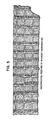
- Such distortions occurring at such low frequency sometimes referred to as "mouseteeth" distortions, are illustrated in the crosshatch pattern of FIGURE 5.
- mouseteeth distortions appear, during and just after the times in which high beam current transients occur, because the deflection circuit, that represents a low impedance energy flywheel during retrace, supplies the transient increase in energy requirement of the ultor circuit.
- energy transferred from the deflection circuit to the ultor circuit may tend to cause variations in the deflection winding trace current.
- a modulation switching current is formed by a bidirectional modulation switch during retrace.
- the modulation switch coupled to the retrace resonant circuit that includes the first retrace capacitance, has a conduction time that is phase modulated during horizontal retrace in accordance with a vertical rate parabolic voltage.
- a second retrace capacitor is coupled in parallel with the modulation switch.
- the modulation switch is conductive during the trace interval and is turned-off at a controllable instant during retrace.
- the modulation switch forms, when conductive, a low impedance across the second retrace capacitor that clamps the voltage across the second retrace capacitor to zero.
- a controllable retrace pulse voltage having an amplitude that is controllable and a width that is variable is developed across the second retrace capacitor when the modulation switch during a portion of retrace is nonconductive.
- the retrace voltage across the second retrace capacitor varies the magnitude of a retrace voltage that is developed across the first retrace capacitor and, in this way, provides the desired deflection winding current modulation so as to correct for outside and inside pincushion distortion.
- mouseteeth distortion is reduced.
- Mouseteeth distortion is reduced because, when the modulation switch is nonconductive during the other portion of horizontal retrace, the flyback transformer primary winding is coupled to the retrace resonant circuit via an impedance formed by the second retrace capacitor.
- impedance is high at low frequencies that are associated with mouseteeth distortion. Such frequencies are substantially lower than the retrace resonant frequency.
- the retrace voltage in a secondary winding of the flyback transformer may be used to provide a synchronizing feedback signal that is used for providing timing information to a phase-control-circuit.
- the phase-control-circuit generates a control signal that synchronizes the horizontal deflection current to a horizontal synchronizing input signal.
- the second retrace capacitance causes the flyback transformer feedback signal to be maintained in phase with respect to the retrace voltage developed across the deflection winding.
- the feedback signal provides correct horizontal timing information of the horizontal deflection current throughout vertical scan.
- a television deflection apparatus embodying an aspect of the invention includes a source of a first input signal at a frequency that is related to a first deflection frequency and a retrace resonant circuit.
- the retrace resonant circuit includes a deflection winding and a first retrace capacitance.
- a deflection current is generated in the deflection winding and a first retrace pulse voltage is generated in the first retrace capacitance during a retrace interval of a given deflection cycle.
- a second retrace capacitance is coupled to the retrace resonant circuit for generating in the second retrace capacitance a second retrace pulse voltage during the retrace interval.
- a supply inductance coupled to a source of an input supply voltage couples the first and second retrace pulse voltages therethrough to a load circuit.
- a source of a modulation second input signal at a frequency that is related to a second deflection frequency is coupled to a switching arrangement. The switching arrangement varies, in accordance with the second input signal, a difference between a time when the second retrace pulse voltage is initiated and a time when the first retrace pulse voltage is initiated to produce a modulation of the deflection current.
- an impedance arrangement that includes the second retrace capacitance, that is high at frequencies that are substantially lower than a retrace resonance frequency of the retrace resonant circuit, is interposed between the supply inductance and the retrace resonant circuit.
- the high impedance isolates the supply inductance from the retrace resonant circuit at the lower frequencies.
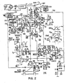
- a horizontal deflection circuit 250 of FIGURE 2 provides horizontal deflection in, for example, an FS color cathode ray tube (CRT) type A66EAS00X01.
- Circuit 250 includes a switching transistor Q1 operating at a horizontal frequency f H and an anti-parallel damper diode D Q1 , both being constructed as one integrated circuit.
- a retrace capacitance C1 is coupled in parallel with transistor Q1 and diode D Q1 .
- a deflection winding L H is coupled in series with an S-shaping trace capacitance C s to form a circuit branch that is coupled in parallel with each of transistor Q1, diode D Q1 and retrace capacitance C1 to form a retrace resonant circuit 100 during horizontal retrace.
- a phase-control stage 101 that includes a horizontal oscillator and a phase detector, not shown in detail in FIGURES, is responsive to a horizontal synchronizing signal H s .
- Signal H s is derived from, for example, a video detector of a television receiver, not shown in the FIGURES.
- Stage 101 applies, via a transistor Q6, a drive voltage 101a to a primary winding T 2a of a driver transformer T2.
- Secondary winding T 2b of transformer T2 is coupled via a voltage divider, that includes resistors R1 and R2, to the base-emitter junction of transistor Q1 for producing a base drive current i b at the horizontal frequency f H .
- a primary winding W1 of a flyback transformer T1 is coupled between a source of a B+ voltage and the collector of transistor Q1.
- a secondary winding W2 of transformer T1 is coupled to stage 101 to provide a feedback retrace signal H r for generating drive signal 101a that synchronizes a horizontal deflection current i2 in winding L H to signal H s .
- a switched raster correction circuit 200 includes an E-W control circuit 300 that controls the switching timing of a switching transistor Q2.
- Transistor Q2 is conductive throughout the trace interval and becomes nonconductive during a controllable instant within the retrace interval.
- the collector of transistor Q2 is coupled to a junction terminal 50 between the emitter of transistor Q1 and retrace capacitor C1.
- the emitter of transistor Q2 is coupled to ground via a small current sampling resistor R101.
- a damper diode D Q2 coupled in parallel with transistor Q2, is constructed with transistor Q2 as one integrated circuit.
- a second retrace capacitor C2 is coupled between the collector of transistor Q2 and ground.
- a retrace voltage V r generated across a winding W4 of transformer T1 provides a high voltage, used for generating an ultor voltage in an ultor power supply 556 that includes rectifying diodes, not shown in the FIGURES.
- a first hypothetical example that is used for explanation purpose represents a first extreme operating condition in which transistor Q2 is maintained conductive throughout trace and retrace.
- deflection circuit 250 generates deflection current i2 in a manner that is well known but without East-West correction. As explained later on, current i2 is at a maximum peak-to-peak amplitude, in this case.
- a second hypothetical example that is also used for explanation purposes, represents a second extreme operating condition in which switching transistor Q2 is in cutoff throughout an entire retrace interval.
- the first one, resonant circuit 100 of FIGURE 2 includes retrace capacitor C1, winding L H and trace capacitor C S .
- the second one includes flyback transformer winding W1 and retrace capacitor C2 that are coupled in series.
- each of the pair of retrace resonant circuits is tuned to a frequency that is lower than a required nominal retrace frequency.
- the resonant circuits are coupled to form a combined resonant circuit. Therefore, the resulting common retrace frequency of the combined resonant circuit is higher than each of its constituents and is made equal to the required nominal retrace frequency that is, illustratively, 43 KHz in the PAL system.
- secondary winding W2 of transformer T1 provides horizontal synchronizing retrace signal H r .
- Each pulse of signal H r represents the retrace interval in deflection winding L H .
- Horizontal synchronizing signal H r is coupled to phase-control-stage 101 for providing feedback synchronization information.
- the synchronization information contained in the pulses of signal H r is indicative of the phase of current i2 in deflection winding L H .
- Signal H r and horizontal sync pulses H s are used to adjust the phase and the frequency of the horizontal oscillator output signal that is included in stage 101.
- primary winding W1 of transformer T1 is coupled to retrace resonant circuit 100 through a capacitive voltage divider that includes capacitors C1 and C2 to form the combined resonant circuit.
- the combined retrace resonant circuit enables proper synchronization without causing mouseteeth distortion.
- the advantages of forming such combined retrace resonant circuit are explained in detail in U.S. Patent 4,634,937 in the name of P.E. Haferl, entitled "EAST-WEST CORRECTION CIRCUIT".
- Retrace voltage V4 developed across winding L H and across capacitor C1, determines the amplitude of deflection current i2.
- Retrace voltage V4 is equal to retrace voltage V1 minus retrace voltage V2. Because current i3 in transistor Q2 is zero during the second portion of retrace when transistor Q2 is nonconductive, retrace current i1 flows substantially entirely as current i4 through capacitor C2 and generates retrace voltage V2.
- modulation of deflection current is obtained by a modulation of the turn-off instant of transistor Q2 during the first half of the retrace interval in a way that mouseteeth distortions are reduced.
- the retrace frequency remains the same during both the first portion of retrace, when transistor Q2 is conductive, and during the second portion of retrace, when transistor Q2 is nonconductive. Consequently, the phase of voltage V1 in winding W1 relative to that of deflection current i2 is unaffected by the conduction state of transistor Q2.
- Modulation of the turn-off instant is permissible because both the retrace time and a retrace voltage V r developed from voltage V1 in winding W4 of transformer T1 are, advantageously, substantially unaffected by the state of conductance of transistor Q2, during retrace.
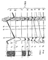
- FIGURES 1a-1h illustrate idealized waveforms useful for explaining the operation of the circuit of FIGURE 2. Similar symbols and numerals in FIGURES 2 and in FIGURES 1a-1h indicate similar items or functions.
- E-W control circuit 300 of FIGURE 2 generates a pulsed voltage V3 which drives the base of transistor Q2.
- Voltage V3 causes transistor Q2 to be conductive throughout the trace interval.
- the falling edge of voltage V3 is phase modulated in the range t2-t3 of FIGURE 1a.
- switching transistor Q2 of FIGURE 2 is conductive prior to time t2 of FIGURE 1a and switched into cut-off after time t2 at the phase modulated instant within the range t2-t3.
- transistor Q2 clamps retrace voltage V2 to zero and varies the instant when the generation of voltage v2 occurs.
- the turn-off time of transistor Q2, determined by the falling edge of voltage V3 of FIGURE 1a, is increasingly delayed within interval t2 - t3.
- the result is a decreasing peak amplitude of voltage V2 of FIGURE 2, an increasing peak amplitude of voltage V4 and an increasing peak amplitude of deflection current i2.
- voltage V2 starts increasing at time t3 of FIGURE 1e and becomes zero at time t5 of each horizontal period.
- deflection current i2 is proportional to retrace voltage V4 and inversely proportional to retrace voltage V2 that is modulated in accordance with the turn-off instant of transistor Q2.
- the falling edge of voltage V3 of FIGURE 1a is phase modulated in a parabolic manner at a vertical rate to obtain the vertical rate envelopes shown in conjunction with waveforms 1e, 1f and 1h.
- the variation of the turn-off time of transistor Q2 of FIGURE 2 modulates also the time when voltage V2 of FIGURE 1e becomes zero near the end of retrace.
- the center of the retrace pulse waveform of voltage V2 during horizontal retrace is maintained the same relative to the center of horizontal retrace time t4 throughout vertical scan.
- voltages V4 and V2 of FIGURE 2 are maintained in phase with respect to voltage V1. It follows that, advantageously, signal H r is maintained in phase with deflection current i2.
- Signal H r developed across winding W2 provides phase information of the phase of deflection current i2.
- Signal H r is applied to stage 101 for synchronizing the horizontal oscillator of stage 101 to sync pulses H s of the video signal. Because capacitor C2 couples winding W1 to winding L H to form a combined resonant circuit, the phase information of signal H r is substantially identical to that of deflection current i2.
- a further advantage provided by the switched operation of transistor Q2 is that inductive components are not required to be coupled in series with transistor Q2. Also, the switched operation of transistor Q2 results in low power dissipation in transistor Q2. Therefore, transistor Q2 may not require a heat sink.
- An additional advantage over other east-west circuits such as a conventional diode modulator is that deflection current i2 does not flow through a damper diode during the second half of trace, resulting in lower deflection losses and lower asymmetric linearity error.
- deflection resonant circuit 100 is coupled to flyback transformer T1 by capacitor C2 having a high impedance, after transistor Q2 becomes nonconductive.
- the ultor voltage rectifying diodes not shown, are conducting.
- the high impedance of capacitor C2 substantially isolates windings L H and W1 at frequencies associated with mouseteeth distortion that are substantially lower than the retrace frequency of resonant circuit 100 during retrace; thereby, raster distortions known as "mouseteeth" are prevented from occurring.
- junction terminal 50 between capacitors C1 and C2 is clamped to ground potential by transistor Q2 during the entire trace interval. Therefore, raster disturbances referred to as "Organ Pipes" do not appear. Organ Pipes type raster disturbances may occur if such clamping were not used as a result of oscillatory current or ringings in the flyback transformer primary current. Such ringings are suppressed because transistor Q1 is clamped to ground by transistor Q2 during the entire trace interval.
- damper diodes D Q1 and D Q2 may be constructed with the corresponding transistor using the integrated circuit technology for further reducing the required discrete components count.
- a protection diode D1 is coupled between the collector of transistor Q2 and a terminal W1a of primary winding W1 of transformer T1.
- Diode D1 protects transistor Q2 from excessive peak voltage that may occur when power is initially turned on.
- Transistor Q2 is protected by diode D1 which limits voltage V2 to a maximum of 350V.
- Transformer T2 has, preferably, 400V isolation capability between the primary and secondary windings.
- a remote control receiver 201 generates an on/off control signal 201a that is coupled to an on/off transistor switch Q7 of a +12V regulator.
- transistor Q7 When transistor Q7 is nonconductive, an output supply voltage +12V is generated that causes phase-control-stage 101 to be energized during power-up operation.
- stage 101 When transistor Q7 is conductive, stage 101 is de-energized that causes stand-by mode operation.
- phase-control-stage 101 supplies base drive to the base of transistor Q6 to cause driver transistor Q6 of transformer T2 to be turned-off.
- on/off control signal 201a is coupled through a resistor R81 and a conductor 555 to the base electrode of a transistor Q5 that provides base drive to transistor Q2, causing transistor Q2 to turn off immediately after the power-on-to-standby transition. Since both transistors Q1 and Q2 are coupled in series, turning off transistor Q2 causes the current in both transistors to cease. Thus transistors Q1 and Q2 are protected. However, such fast shut-down arrangement may require a fast spot suppression circuit to prevent beam spot related damage to the CRT, not shown.
- FIGURE 2 An alternative protection arrangement, which advantageously, may not require fast spot suppression is also shown in FIGURE 2.
- a feedback arrangement that includes a series arrangement of a diode D10 and a resistor R91 is coupled between the emitter of transistor Q2, as shown by the dashed line, and the base of transistor Q5, via conductor 555.
- the emitter of transistor Q2 is coupled to ground via current sampling resistor R101, causing current i3 to be sampled across resistor R101.
- a resulting voltage V oc developed across resistor R101 controls the base voltage of transistor Q5.
- transistor Q5 is turned on by voltage V oc and reduces the base drive of transistor Q2.
- current i3 is limited to a peak of 1.8 ampere when, for example, resistor R101 equals 1 ohm.
- the feedback provided by diode D10 and resistor R91 advantageously, protects both transistors Q1 and Q2 that are coupled in series during operation and, in particular, during the power-up-to-standby transition. It should be understood that such feedback arrangement may also be used together with, or instead of the arrangement in which signal 201a is coupled to the base of transistor Q5 that was explained before. When, for example, both arrangements are used together, current i3 may become substantially reduced to, for example, zero for providing the required over-current protection or for providing on/off operation.
- FIGURE 6a illustrates an envelope of a waveform of current i3 of FIGURE 2 immediately after corresponding transitions between normal operation power-up mode and standby mode without the protection circuit, that would occur if conductor 555 were disconnected for disabling the operation of the protection circuit.
- FIGURE 6b illustrates the envelope of the waveform of current i3 of FIGURE 2 when conductor 555 is connected that enables the operation of the protection circuit. Note that current i3 of FIGURE 6b is limited to the maximum of 1.8 amperes.
- FIGURE 6c illustrates an envelope of collector current of Q1 when the protection circuit is disabled and FIGURE 6d illustrates the envelope of collector current of Q1 when the protection circuit is enabled.
- the operation of the protection circuit is also discussed in U.K. Patent Application 8805757, entitled PROTECTION ARRANGEMENT OF A DEFLECTION CIRCUIT, in the name of the same Applicant, filed 10 March 1988.
- E-W control circuit 300 of FIGURE 2 includes a differential amplifier formed by transistors Q3 and Q4 and Darlington driver transistor Q5 which drives switching transistor Q2.
- the differential amplifier that includes transistors Q3 and Q4 compares a vertical parabola voltage V6 to an exponentially shaped ramp portion V 5a of a voltage V5 having a waveform that is shown in FIGURE 2.
- the crossover points of the compared voltages determines the timing of control voltage V3 of FIGURE 1a.
- horizontal retrace pulses H w3 of FIGURE 2 developed in a winding W3 of transformer T1 are coupled via a resistor R4 to a zener diode D3.
- a speed-up network that includes a capacitor C4, a resistor R5 and a diode D2 generates a gating pulse V D3 across diode D3 having a leading edge with a fast rise time. Faster leading edge, results,advantageously, in a larger dynamic range of E-W control circuit 300.
- Pulse V D3 across diode D3 is applied via resistors R6 and R7 to a capacitor C5 and to a resistor R9 for generating the exponentially shaped ramp portion V 5a of voltage V5.
- Pulsed voltage V5 that includes exponentially increasing top portion V 5a is applied to the base of transistor Q4.
- a vertical rate parabolic voltage V p of FIGURE 2 that includes a superimposed sawtooth voltage is coupled from a DC blocking capacitor C c of a conventional vertical deflection circuit 350 to the base of transistor Q3 via a capacitor C8, a resistor R20 and a resistor R19.
- Resistors R14, R15 and R16 provide dc bias to the base of transistor Q3.
- Voltage V2 that is coupled via a resistor R13 to the base of transistor Q3 and to an integrating capacitor C6 provides a negative feedback, causing the vertical rate envelope of voltage V2 to track parabolic voltage V p that is developed in capacitor C c .
- a vertical sawtooth voltage V RS developed across a sampling resistor R s is coupled, via a resistor R10 and a resistor R9, to a capacitor C5 for developing a voltage V7 having an exponential upramping portion at a peak amplitude that is determined by voltage V RS .
- Voltage V7 is coupled to the base of transistor Q4 of E-W control circuit 300. In this way, Voltage V RS is also coupled via capacitor C c to the base of transistor Q3. Because voltage V RS is applied in a differential manner, voltage V RS is prevented from substantially affecting the switching operation of transistors Q3 and Q4.
- a vertical parabola voltage V 6 developed at the base of transistor Q3 is compared to horizontal ramp voltage V5. The crossover points of voltages V5 and V6 determine the timing of the leading and trailing edges of voltage V3, as indicated before.
- Exponentially shaped ramp portion V 5a of voltage V5 linearizes the east-west raster correction or modulator circuit 200 by compensating for the decreasing level of current i1 of FIGURE 1b, during retrace.
- Linearization occurs because a small amount of modulation of voltage V3 near time t2 of FIGURE 1a results in a higher amplitude modulation of voltage V2 of FIGURE 1e than the same amount of modulation of voltage V3 near time t3 of FIGURE 1a. This is so because the amplitude of each of currents i1 and i4 of FIGURES 1b and 1d, respectively, is higher at time t2 than at time t3 and because voltage V2 is proportional to the value of ⁇ i4. dt.
- the exponentially shaped ramp voltage V5 is steeper near time t2 than at time t3 of FIGURE 1g. Consequently, for a given voltage variation at the base of transistor Q3, the modulation of voltage V3 is smaller around time t2 than around time t3.
- the exponentially shaped ramp portion V 5a of voltage V5 linearizes the operation of E-W raster correction circuit 200.
- Resistor R15 raises the dc average of voltage V5. Compensation of picture width variations as a function of beam current, that may be referred to as anti-breathing, may be applied via the base of transistor Q3.
- FIGURES 3a-3b and 4 illustrate waveforms obtained in operating horizontal deflection circuit 250 of FIGURE 2. Similar symbols and numerals in FIGURES 1a-1h, 2, 3a-3b and 4 indicate similar items or functions.
- voltage V1 of FIGURE 3a and current i1 are substantially unmodulated.
- transistor Q2 of FIGURE 2 is switched to cutoff.
- Diode D Q2 starts conducting between time t5 and t6 of FIGURE 3b.
- voltage V2 of FIGURE 3b is centered around the center of voltage V1 of FIGURE 3a.
- current i3 of FIGURE 3b is zero. Note that deflection current i2 of FIGURE 4 is modulated to provide outside pincushion distortion correction.
- Transistor Q5 of FIGURE 2 having a base that is coupled to the junction of a load resistor R12 and a collector of transistor Q3, applies a base drive to transistor Q2 from a load resistor R17 that is coupled to the collector of transistor Q5.
- the collector of transistor Q5 is coupled via a parallel arrangement of a capacitor C7 and a resistor R18 for generating a fast transition of a falling edge portion of voltage V3 to obtain a fast turn-off of transistor Q2.
- the fast turn-off allows interrupting current i3 immediately after time t1 of FIGURE 1c and allows using the full modulation range between time t1 and t4.
- the turn-off delay of transistor Q2 of FIGURE 2 is less than 1 microsecond.
- the use of a MOSFET in place of Q2 may further reduce the turn-off delay.
- the fast turn-off feature may be desirable in a situation that requires a deflection current at, for example, a higher frequency such as 2xf H .
- FIGURE 7 illustrates a horizontal deflection circuit 250′ that is similar to circuit 250 of FIGURE 2 and that is used for providing horizontal scanning in, for example, a Philips 45AX Picture tube, not shown. Similar numbers and symbols in FIGURES 7 and 2 indicate similar items or functions.
- circuit 250′ of FIGURE 7 provides, in addition to outside pincushion correction that is provided as explained before with respect to FIGURE 2, also inside pincushion correction. Inside pincushion correction is obtained by the operation of a resonance circuit 60 that includes an inductor L1, a capacitor C′ S and that is coupled to a resistor R22.
- Current i5 modulates the trace voltage across capacitor C S .
- the amount of inside correction may be adjusted by adjusting the value of inductor L1. This adjustment, however, is not critical, and a fixed coil of, for example, 2.2mH may be used.
- the required value of capacitor C2 of FIGURE 7 is greater than that in the circuit of FIGURE 2 because inductor L1 of FIGURE 7 is coupled in parallel with winding W1 of transformer T1 during retrace.
- a current such as current i5 is modulated to provide inside pincushion correction is described in more detail in U.S. Patent No. 4,719,392, entitled RASTER CORRECTION CIRCUIT, in the name of P.E. Haferl.
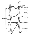
- FIGURES 8a-8c illustrate waveforms obtained during operation of circuit 250′ of FIGURE 7. Similar numerals and symbols in FIGURES 8a-8c and 7 illustrate similar items or functions. Note that current i3 of FIGURE 8b is anti-"S"-shaped during trace, as a result of current i5 of FIGURE 7. Without inside pincushion correction, current i3 would have basically increased in a linear manner, as ideally shown in FIGURE 1c.
- transistor Q2 of FIGURE 7 also provides a current path for current i5, during trace. Note that both currents i5 of FIGURE 8a and current i3 of FIGURE 8b are modulated to provide inside pincushion distortion correction.
Landscapes
- Engineering & Computer Science (AREA)
- Multimedia (AREA)
- Signal Processing (AREA)
- Details Of Television Scanning (AREA)
Abstract
Description
- This invention relates to a deflection circuit in which the amplitude of a deflection current may be varied or modulated over a relatively wide range for correcting a raster distortion. Modulation of the deflection current amplitude may be desirable for purposes such as, for example, correction of outside and of inside east-west pincushion distortion.
- Typically, the horizontal deflection circuit includes an output stage having a deflection switch, a horizontal deflection winding and a trace capacitance that supplies deflection current to the deflection winding during each trace interval. A first retrace capacitance is coupled across the deflection winding during the retrace interval to form a retrace resonant circuit. Energy is replenished during retrace via a flyback transformer.
- A high beam current provided from a secondary winding of the flyback transformer, during display, for example, of each white horizontal strip of a crosshatch pattern, such as shown in FIGURE 5, represents a heavy load to the flyback transformer during retrace.
- In some prior art circuits, the retrace resonant circuit is coupled via a relatively small output impedance, of an east-west control circuit, to the primary winding of the flyback transformer throughout retrace. In such prior art circuits, the retrace capacitance may be slightly discharged during retrace due to the aforementioned loading. This may result in a discharge current from the trace capacitance into the retrace capacitance through the deflection winding and a resulting slight drop of the voltage across the trace capacitance due to the white horizontal strips of the crosshatch pattern.
- The charge of the trace capacitance is replenished during the retrace intervals associated with the scan lines that display the black picture portion underneath the white crosshatch stripes. This causes a small current in the opposite direction, at a low frequency, to flow through the deflection winding during the trace intervals. The charge and discharge current of the trace capacitance produces a small raster displacement and results in low frequency oscillations modulating the deflection winding trace current. This low frequency modulation may cause each vertical strip of the crosshatch pattern to have of a zig-zag shape, instead of a straight line shape. The zig-zag shape appears in a given vertical direction immediately below the intersection point with a horizontal strip. Such distortions occurring at such low frequency, sometimes referred to as "mouseteeth" distortions, are illustrated in the crosshatch pattern of FIGURE 5.
- Thus, mouseteeth distortions appear, during and just after the times in which high beam current transients occur, because the deflection circuit, that represents a low impedance energy flywheel during retrace, supplies the transient increase in energy requirement of the ultor circuit. Thus, energy transferred from the deflection circuit to the ultor circuit may tend to cause variations in the deflection winding trace current. The nature of mouseteeth distortion and corresponding solutions are explained in U.S. Patents 4,429,257; 4,634,937; 4,780,648 and 4,794,307.
- In a horizontal deflection circuit, embodying an aspect of the invention, a modulation switching current is formed by a bidirectional modulation switch during retrace. The modulation switch, coupled to the retrace resonant circuit that includes the first retrace capacitance, has a conduction time that is phase modulated during horizontal retrace in accordance with a vertical rate parabolic voltage. A second retrace capacitor is coupled in parallel with the modulation switch. The modulation switch is conductive during the trace interval and is turned-off at a controllable instant during retrace. The modulation switch forms, when conductive, a low impedance across the second retrace capacitor that clamps the voltage across the second retrace capacitor to zero. As a result, a controllable retrace pulse voltage having an amplitude that is controllable and a width that is variable is developed across the second retrace capacitor when the modulation switch during a portion of retrace is nonconductive. The retrace voltage across the second retrace capacitor varies the magnitude of a retrace voltage that is developed across the first retrace capacitor and, in this way, provides the desired deflection winding current modulation so as to correct for outside and inside pincushion distortion.
- Advantageously, by having the modulation switch conductive during only a portion of horizontal retrace, mouseteeth distortion is reduced. Mouseteeth distortion is reduced because, when the modulation switch is nonconductive during the other portion of horizontal retrace, the flyback transformer primary winding is coupled to the retrace resonant circuit via an impedance formed by the second retrace capacitor. Such impedance is high at low frequencies that are associated with mouseteeth distortion. Such frequencies are substantially lower than the retrace resonant frequency. By operating the modulation switch in the switching mode, power dissipation is, advantageously, reduced.
- The retrace voltage in a secondary winding of the flyback transformer may be used to provide a synchronizing feedback signal that is used for providing timing information to a phase-control-circuit. The phase-control-circuit generates a control signal that synchronizes the horizontal deflection current to a horizontal synchronizing input signal.
- In accordance with a feature of the invention, the second retrace capacitance causes the flyback transformer feedback signal to be maintained in phase with respect to the retrace voltage developed across the deflection winding. Thus, the feedback signal provides correct horizontal timing information of the horizontal deflection current throughout vertical scan. Had the retrace voltages in the flyback transformer and in the deflection winding not been maintained in phase during the entire vertical scan, a raster distortion resulting in a slightly parabolically bent raster in the vertical direction might have occurred.
- A television deflection apparatus embodying an aspect of the invention includes a source of a first input signal at a frequency that is related to a first deflection frequency and a retrace resonant circuit. The retrace resonant circuit includes a deflection winding and a first retrace capacitance. A deflection current is generated in the deflection winding and a first retrace pulse voltage is generated in the first retrace capacitance during a retrace interval of a given deflection cycle. A second retrace capacitance is coupled to the retrace resonant circuit for generating in the second retrace capacitance a second retrace pulse voltage during the retrace interval. A supply inductance coupled to a source of an input supply voltage couples the first and second retrace pulse voltages therethrough to a load circuit. A source of a modulation second input signal at a frequency that is related to a second deflection frequency is coupled to a switching arrangement. The switching arrangement varies, in accordance with the second input signal, a difference between a time when the second retrace pulse voltage is initiated and a time when the first retrace pulse voltage is initiated to produce a modulation of the deflection current. When the second retrace pulse voltage is generated, an impedance arrangement, that includes the second retrace capacitance, that is high at frequencies that are substantially lower than a retrace resonance frequency of the retrace resonant circuit, is interposed between the supply inductance and the retrace resonant circuit. The high impedance isolates the supply inductance from the retrace resonant circuit at the lower frequencies.
- In the Drawing:
- FIGURES 1a-1h illustrate idealized waveforms useful in explaining the circuit of FIGURE 2;
- FIGURE 2 illustrates a deflection circuit, embodying an aspect of the invention, that includes outside pincushion distortion correction;
- FIGURES 3a-3b illustrate waveforms occurring during horizontal retrace that are useful in explaining the circuit of FIGURE 2;
- FIGURE 4 illustrates additional waveforms that are useful in explaining the operation of the circuit of FIGURE 2;
- FIGURE 5 illustrates a crosshatch pattern in which "mouseteeth" distortion is uncorrected;
- FIGURES 6a-6d illustrate waveforms useful in explaining a current protection feature of the circuit of FIGURE 2;
- FIGURE 7 illustrates a second embodiment of the invention that includes inside pincushion distortion correction; and
- FIGURES 8a-8c illustrate waveforms associated with the circuit of FIGURE 7.
- A
horizontal deflection circuit 250 of FIGURE 2, embodying an aspect of the invention, provides horizontal deflection in, for example, an FS color cathode ray tube (CRT) type A66EAS00X01.Circuit 250 includes a switching transistor Q1 operating at a horizontal frequency fH and an anti-parallel damper diode DQ1, both being constructed as one integrated circuit. A retrace capacitance C1 is coupled in parallel with transistor Q1 and diode DQ1. A deflection winding LH is coupled in series with an S-shaping trace capacitance Cs to form a circuit branch that is coupled in parallel with each of transistor Q1, diode DQ1 and retrace capacitance C1 to form a retraceresonant circuit 100 during horizontal retrace. - A phase-
control stage 101 that includes a horizontal oscillator and a phase detector, not shown in detail in FIGURES, is responsive to a horizontal synchronizing signal Hs. Signal Hs is derived from, for example, a video detector of a television receiver, not shown in the FIGURES.Stage 101 applies, via a transistor Q6, a drive voltage 101a to a primary winding T2a of a driver transformer T2. Secondary winding T2b of transformer T2 is coupled via a voltage divider, that includes resistors R1 and R2, to the base-emitter junction of transistor Q1 for producing a base drive current ib at the horizontal frequency fH. A primary winding W₁ of a flyback transformer T1 is coupled between a source of a B+ voltage and the collector of transistor Q1. A secondary winding W₂ of transformer T1 is coupled tostage 101 to provide a feedback retrace signal Hr for generating drive signal 101a that synchronizes a horizontal deflection current i₂ in winding LH to signal Hs. - A switched
raster correction circuit 200, embodying a feature of the invention, includes anE-W control circuit 300 that controls the switching timing of a switching transistor Q2. Transistor Q2 is conductive throughout the trace interval and becomes nonconductive during a controllable instant within the retrace interval. The collector of transistor Q2 is coupled to ajunction terminal 50 between the emitter of transistor Q1 and retrace capacitor C1. The emitter of transistor Q2 is coupled to ground via a small current sampling resistor R101. A damper diode DQ2 ,coupled in parallel with transistor Q2, is constructed with transistor Q2 as one integrated circuit. A second retrace capacitor C2 is coupled between the collector of transistor Q2 and ground. A retrace voltage Vr generated across a winding W₄ of transformer T1 provides a high voltage, used for generating an ultor voltage in anultor power supply 556 that includes rectifying diodes, not shown in the FIGURES. - A first hypothetical example that is used for explanation purpose represents a first extreme operating condition in which transistor Q2 is maintained conductive throughout trace and retrace. In this case,
deflection circuit 250 generates deflection current i₂ in a manner that is well known but without East-West correction. As explained later on, current i₂ is at a maximum peak-to-peak amplitude, in this case. - A second hypothetical example that is also used for explanation purposes, represents a second extreme operating condition in which switching transistor Q2 is in cutoff throughout an entire retrace interval. In the second example, during retrace, a pair of resonant circuits are formed. The first one,
resonant circuit 100 of FIGURE 2, includes retrace capacitor C1, winding LH and trace capacitor CS. The second one includes flyback transformer winding W₁ and retrace capacitor C2 that are coupled in series. Considered separately, each of the pair of retrace resonant circuits is tuned to a frequency that is lower than a required nominal retrace frequency. The resonant circuits are coupled to form a combined resonant circuit. Therefore, the resulting common retrace frequency of the combined resonant circuit is higher than each of its constituents and is made equal to the required nominal retrace frequency that is, illustratively, 43 KHz in the PAL system. - As explained before, secondary winding W₂ of transformer T1 provides horizontal synchronizing retrace signal Hr. Each pulse of signal Hr represents the retrace interval in deflection winding LH. Horizontal synchronizing signal Hr is coupled to phase-control-
stage 101 for providing feedback synchronization information. The synchronization information contained in the pulses of signal Hr is indicative of the phase of current i₂ in deflection winding LH. Signal Hr and horizontal sync pulses Hs are used to adjust the phase and the frequency of the horizontal oscillator output signal that is included instage 101. - In the second hypothetical example, primary winding W₁ of transformer T1 is coupled to retrace
resonant circuit 100 through a capacitive voltage divider that includes capacitors C1 and C2 to form the combined resonant circuit. The combined retrace resonant circuit enables proper synchronization without causing mouseteeth distortion. The advantages of forming such combined retrace resonant circuit are explained in detail in U.S. Patent 4,634,937 in the name of P.E. Haferl, entitled "EAST-WEST CORRECTION CIRCUIT". - During trace, current i₁ in winding W₁ flows through transistor Q1 and through transistor Q2 to ground. During retrace, current i₁ that flows through capacitor C1 also flows through capacitor C2 as retrace current i₄ and causes a retrace voltage V₂ to be developed across retrace capacitor C2.
- The amplitude of a retrace voltage V₁, developed across the series coupled capacitor C1 and C2 is stabilized by the B+ voltage that is regulated. Therefore, voltage V₁ is, advantageously, substantially unaffected by the East-West modulation. Retrace voltage V₄, developed across winding LH and across capacitor C1, determines the amplitude of deflection current i₂. Retrace voltage V₄ is equal to retrace voltage V₁ minus retrace voltage V₂. Because current i₃ in transistor Q2 is zero during the second portion of retrace when transistor Q2 is nonconductive, retrace current i₁ flows substantially entirely as current i₄ through capacitor C2 and generates retrace voltage V₂. It follows that in the second hypothetical example in which transistor Q2 is nonconductive throughout retrace, voltage V₂ is at a maximum amplitude. Consequently, voltage V₄ amplitude is at a minimum and deflection current i₂ is also at a minimum in the second hypothetical example.
- In accordance with an aspect of the invention, modulation of deflection current is obtained by a modulation of the turn-off instant of transistor Q2 during the first half of the retrace interval in a way that mouseteeth distortions are reduced. By selecting the value of capacitor C1 to be, for example, approximately twice that of capacitor C2, and the value of the inductance of winding W₁ to be approximately twice that of winding LH, the retrace frequency remains the same during both the first portion of retrace, when transistor Q2 is conductive, and during the second portion of retrace, when transistor Q2 is nonconductive. Consequently, the phase of voltage V₁ in winding W₁ relative to that of deflection current i₂ is unaffected by the conduction state of transistor Q2. Modulation of the turn-off instant is permissible because both the retrace time and a retrace voltage Vr developed from voltage V₁ in winding W₄ of transformer T1 are, advantageously, substantially unaffected by the state of conductance of transistor Q2, during retrace.
- FIGURES 1a-1h illustrate idealized waveforms useful for explaining the operation of the circuit of FIGURE 2. Similar symbols and numerals in FIGURES 2 and in FIGURES 1a-1h indicate similar items or functions.
-
E-W control circuit 300 of FIGURE 2 generates a pulsed voltage V₃ which drives the base of transistor Q2. Voltage V₃ causes transistor Q2 to be conductive throughout the trace interval. During retrace, the falling edge of voltage V₃ is phase modulated in the range t₂-t₃ of FIGURE 1a. Thus, switching transistor Q2 of FIGURE 2 is conductive prior to time t₂ of FIGURE 1a and switched into cut-off after time t₂ at the phase modulated instant within the range t₂-t₃. When conductive, transistor Q2 clamps retrace voltage V₂ to zero and varies the instant when the generation of voltage v₂ occurs. - Current i₁ in winding W₁ of transformer T1 of FIGURE 2 flows into
resonant circuit 100 that includes winding LH and capacitor C1. Fromresonant circuit 100, current i₁ splits and forms current i₃ and current i₄ when transistor Q2 of FIGURE 2 is nonconductive. When transistor Q2 is turned-off, the decreasing current i₄ of FIGURE 1d charges capacitor C2 of FIGURE 2 until time t₄ of FIGURE 1d, occuring at the center of the retrace interval when currents i₁ and i₄ become zero. As a result, voltage V₂ of FIGURE 1e reaches its peak amplitude at the center of retrace. During the second half of retrace, negative current i₄ of FIGURE 1d, that becomes increasingly more negative, discharges capacitor C2 of FIGURE 2 until voltage V₂ becomes negative. When voltage V₂ becomes sufficiently negative, diode DQ2 starts conducting and clamps voltage V₂ to -0.6 voltage, the forward voltage of diode DQ2. - The correction of outside pincushion distortion requires a higher amplitude of deflection current i₂ when scanning lines at the center of the raster than at the top or bottom. At the top of the raster, transistor Q2 is turned off at time t₂ of FIGURE 1a, that is the earliest. Voltage V₂ of FIGURE 1e starts to increase after time t₂. After the center of retrace occurs, voltage V₂ decreases until it becomes zero at time t₆. Because transistor Q2 is turned off at the time t₂ at the top of the raster, the peak amplitude of voltage V₂ is at a maximum; consequently, the peak amplitude of voltage V₄ of FIGURE 1f is at a minimum. From the top toward the center of the raster, the turn-off time of transistor Q2, determined by the falling edge of voltage V₃ of FIGURE 1a, is increasingly delayed within interval t₂ - t₃. The result is a decreasing peak amplitude of voltage V₂ of FIGURE 2, an increasing peak amplitude of voltage V₄ and an increasing peak amplitude of deflection current i₂. At the center of the raster, voltage V₂ starts increasing at time t₃ of FIGURE 1e and becomes zero at time t₅ of each horizontal period. From the center toward the bottom of the raster, the turn-off time of transistor Q2 of FIGURE 2 is increasingly advanced from time t₃ to time t₂ of FIGURE 1a, resulting in an increasing voltage V₂ of FIGURE 2, a decreasing voltage V₄ and a decreasing deflection current i₂. Thus, deflection current i₂ is proportional to retrace voltage V₄ and inversely proportional to retrace voltage V₂ that is modulated in accordance with the turn-off instant of transistor Q2.
- The falling edge of voltage V₃ of FIGURE 1a is phase modulated in a parabolic manner at a vertical rate to obtain the vertical rate envelopes shown in conjunction with waveforms 1e, 1f and 1h. Advantageously, the variation of the turn-off time of transistor Q2 of FIGURE 2 modulates also the time when voltage V₂ of FIGURE 1e becomes zero near the end of retrace.
- In accordance with an inventive feature, the center of the retrace pulse waveform of voltage V₂ during horizontal retrace is maintained the same relative to the center of horizontal retrace time t₄ throughout vertical scan. Thus, voltages V₄ and V₂ of FIGURE 2 are maintained in phase with respect to voltage V₁. It follows that, advantageously, signal Hr is maintained in phase with deflection current i₂.
- Signal Hr developed across winding W₂ provides phase information of the phase of deflection current i₂. Signal Hr is applied to stage 101 for synchronizing the horizontal oscillator of
stage 101 to sync pulses Hs of the video signal. Because capacitor C2 couples winding W₁ to winding LH to form a combined resonant circuit, the phase information of signal Hr is substantially identical to that of deflection current i₂. A further advantage provided by the switched operation of transistor Q2 is that inductive components are not required to be coupled in series with transistor Q2. Also, the switched operation of transistor Q2 results in low power dissipation in transistor Q2. Therefore, transistor Q2 may not require a heat sink. An additional advantage over other east-west circuits such as a conventional diode modulator is that deflection current i₂ does not flow through a damper diode during the second half of trace, resulting in lower deflection losses and lower asymmetric linearity error. - As explained before, during retrace, deflection
resonant circuit 100 is coupled to flyback transformer T1 by capacitor C2 having a high impedance, after transistor Q2 becomes nonconductive. When transistor Q2 becomes nonconductive, the ultor voltage rectifying diodes, not shown, are conducting. The high impedance of capacitor C2 substantially isolates windings LH and W₁ at frequencies associated with mouseteeth distortion that are substantially lower than the retrace frequency ofresonant circuit 100 during retrace; thereby, raster distortions known as "mouseteeth" are prevented from occurring. - In accordance with a feature of the invention,
junction terminal 50 between capacitors C1 and C2 is clamped to ground potential by transistor Q2 during the entire trace interval. Therefore, raster disturbances referred to as "Organ Pipes" do not appear. Organ Pipes type raster disturbances may occur if such clamping were not used as a result of oscillatory current or ringings in the flyback transformer primary current. Such ringings are suppressed because transistor Q1 is clamped to ground by transistor Q2 during the entire trace interval. - Advantageously, damper diodes DQ1 and DQ2 may be constructed with the corresponding transistor using the integrated circuit technology for further reducing the required discrete components count.
- A protection diode D1 is coupled between the collector of transistor Q2 and a terminal W1a of primary winding W₁ of transformer T1. Diode D1 protects transistor Q2 from excessive peak voltage that may occur when power is initially turned on. Transistor Q2 is protected by diode D1 which limits voltage V₂ to a maximum of 350V. Transformer T2 has, preferably, 400V isolation capability between the primary and secondary windings.
- A
remote control receiver 201 generates an on/off control signal 201a that is coupled to an on/off transistor switch Q7 of a +12V regulator. When transistor Q7 is nonconductive, an output supply voltage +12V is generated that causes phase-control-stage 101 to be energized during power-up operation. When transistor Q7 is conductive,stage 101 is de-energized that causes stand-by mode operation. During a transition to the stand-by mode of operation, phase-control-stage 101 supplies base drive to the base of transistor Q6 to cause driver transistor Q6 of transformer T2 to be turned-off. - After, for example, the transition from normal or power-up operation to the stand-by mode operation there may still be energy stored in primary winding T2a of transformer T2 of FIGURE 2. This energy may continue producing base current ib in deflection transistor Q1 until a magnitude of voltage 101a across primary winding T2a of transformer T2 decreases to zero. As a result, a final deflection cycle may be generated with an extended but undefined time duration that ends when transistor Q1 ceases to conduct. Consequently, currents i₁, i₂ and i₃ might increase excessively and destroy transistors Q1 and Q2.
- To prevent such a possibility, on/off control signal 201a is coupled through a resistor R81 and a
conductor 555 to the base electrode of a transistor Q5 that provides base drive to transistor Q2, causing transistor Q2 to turn off immediately after the power-on-to-standby transition. Since both transistors Q1 and Q2 are coupled in series, turning off transistor Q2 causes the current in both transistors to cease. Thus transistors Q1 and Q2 are protected. However, such fast shut-down arrangement may require a fast spot suppression circuit to prevent beam spot related damage to the CRT, not shown. - An alternative protection arrangement, which advantageously, may not require fast spot suppression is also shown in FIGURE 2. In such preferred arrangement, a feedback arrangement that includes a series arrangement of a diode D10 and a resistor R91 is coupled between the emitter of transistor Q2, as shown by the dashed line, and the base of transistor Q5, via
conductor 555. When such feedback arrangement is used, the emitter of transistor Q2 is coupled to ground via current sampling resistor R101, causing current i₃ to be sampled across resistor R101. A resulting voltage Voc developed across resistor R101 controls the base voltage of transistor Q5. When voltage Voc across resistor R101 exceeds +1.8V, transistor Q5 is turned on by voltage Voc and reduces the base drive of transistor Q2. Thus, current i₃ is limited to a peak of 1.8 ampere when, for example, resistor R101 equals 1 ohm. - The feedback provided by diode D10 and resistor R91, advantageously, protects both transistors Q1 and Q2 that are coupled in series during operation and, in particular, during the power-up-to-standby transition. It should be understood that such feedback arrangement may also be used together with, or instead of the arrangement in which signal 201a is coupled to the base of transistor Q5 that was explained before. When, for example, both arrangements are used together, current i₃ may become substantially reduced to, for example, zero for providing the required over-current protection or for providing on/off operation.
- FIGURE 6a illustrates an envelope of a waveform of current i₃ of FIGURE 2 immediately after corresponding transitions between normal operation power-up mode and standby mode without the protection circuit, that would occur if
conductor 555 were disconnected for disabling the operation of the protection circuit. Similarly, FIGURE 6b illustrates the envelope of the waveform of current i₃ of FIGURE 2 whenconductor 555 is connected that enables the operation of the protection circuit. Note that current i₃ of FIGURE 6b is limited to the maximum of 1.8 amperes. Likewise, FIGURE 6c illustrates an envelope of collector current of Q1 when the protection circuit is disabled and FIGURE 6d illustrates the envelope of collector current of Q1 when the protection circuit is enabled. The operation of the protection circuit is also discussed in U.K. Patent Application 8805757, entitled PROTECTION ARRANGEMENT OF A DEFLECTION CIRCUIT, in the name of the same Applicant, filed 10 March 1988. -
E-W control circuit 300 of FIGURE 2 includes a differential amplifier formed by transistors Q3 and Q4 and Darlington driver transistor Q5 which drives switching transistor Q2. The differential amplifier that includes transistors Q3 and Q4 compares a vertical parabola voltage V₆ to an exponentially shaped ramp portion V5a of a voltage V₅ having a waveform that is shown in FIGURE 2. The crossover points of the compared voltages determines the timing of control voltage V₃ of FIGURE 1a. - To develop voltage V₅ of FIGURE 2, horizontal retrace pulses Hw3 of FIGURE 2, developed in a winding W₃ of transformer T1, are coupled via a resistor R4 to a zener diode D3. A speed-up network that includes a capacitor C4, a resistor R5 and a diode D2 generates a gating pulse VD3 across diode D3 having a leading edge with a fast rise time. Faster leading edge, results,advantageously, in a larger dynamic range of
E-W control circuit 300. Pulse VD3 across diode D3 is applied via resistors R6 and R7 to a capacitor C5 and to a resistor R9 for generating the exponentially shaped ramp portion V5a of voltage V5. Pulsed voltage V5 that includes exponentially increasing top portion V5a is applied to the base of transistor Q4. A vertical rate parabolic voltage Vp of FIGURE 2 that includes a superimposed sawtooth voltage is coupled from a DC blocking capacitor Cc of a conventionalvertical deflection circuit 350 to the base of transistor Q3 via a capacitor C8, a resistor R20 and a resistor R19. Resistors R14, R15 and R16 provide dc bias to the base of transistor Q3. Voltage V₂ that is coupled via a resistor R13 to the base of transistor Q3 and to an integrating capacitor C6 provides a negative feedback, causing the vertical rate envelope of voltage V₂ to track parabolic voltage Vp that is developed in capacitor Cc. - A vertical sawtooth voltage VRS developed across a sampling resistor Rs is coupled, via a resistor R10 and a resistor R9, to a capacitor C5 for developing a voltage V₇ having an exponential upramping portion at a peak amplitude that is determined by voltage VRS. Voltage V₇ is coupled to the base of transistor Q4 of
E-W control circuit 300. In this way, Voltage VRS is also coupled via capacitor Cc to the base of transistor Q3. Because voltage VRS is applied in a differential manner, voltage VRS is prevented from substantially affecting the switching operation of transistors Q3 and Q4. A vertical parabola voltage V6 developed at the base of transistor Q3 is compared to horizontal ramp voltage V₅. The crossover points of voltages V₅ and V₆ determine the timing of the leading and trailing edges of voltage V₃, as indicated before. - Exponentially shaped ramp portion V5a of voltage V₅ linearizes the east-west raster correction or
modulator circuit 200 by compensating for the decreasing level of current i₁ of FIGURE 1b, during retrace. Linearization occurs because a small amount of modulation of voltage V₃ near time t₂ of FIGURE 1a results in a higher amplitude modulation of voltage V₂ of FIGURE 1e than the same amount of modulation of voltage V₃ near time t₃ of FIGURE 1a. This is so because the amplitude of each of currents i₁ and i₄ of FIGURES 1b and 1d, respectively, is higher at time t₂ than at time t₃ and because voltage V₂ is proportional to the value of ∫i₄. dt. The exponentially shaped ramp voltage V₅ is steeper near time t₂ than at time t₃ of FIGURE 1g. Consequently, for a given voltage variation at the base of transistor Q3, the the modulation of voltage V₃ is smaller around time t₂ than around time t₃. Thus the exponentially shaped ramp portion V5a of voltage V₅ linearizes the operation of E-Wraster correction circuit 200. Resistor R15 raises the dc average of voltage V₅. Compensation of picture width variations as a function of beam current, that may be referred to as anti-breathing, may be applied via the base of transistor Q3. - FIGURES 3a-3b and 4 illustrate waveforms obtained in operating
horizontal deflection circuit 250 of FIGURE 2. Similar symbols and numerals in FIGURES 1a-1h, 2, 3a-3b and 4 indicate similar items or functions. Advantageously, voltage V₁ of FIGURE 3a and current i₁ are substantially unmodulated. Between time t₂ and t₃ of FIGURE 3b transistor Q2 of FIGURE 2 is switched to cutoff. Diode DQ2 starts conducting between time t₅ and t₆ of FIGURE 3b. Advantageously, voltage V₂ of FIGURE 3b is centered around the center of voltage V₁ of FIGURE 3a. When voltage V₂ of FIGURE 3b is generated, current i₃ of FIGURE 3b is zero. Note that deflection current i₂ of FIGURE 4 is modulated to provide outside pincushion distortion correction. - Transistor Q5 of FIGURE 2, having a base that is coupled to the junction of a load resistor R12 and a collector of transistor Q3, applies a base drive to transistor Q2 from a load resistor R17 that is coupled to the collector of transistor Q5. The collector of transistor Q5 is coupled via a parallel arrangement of a capacitor C7 and a resistor R18 for generating a fast transition of a falling edge portion of voltage V₃ to obtain a fast turn-off of transistor Q2. The fast turn-off allows interrupting current i₃ immediately after time t₁ of FIGURE 1c and allows using the full modulation range between time t₁ and t₄. Illustratively, the turn-off delay of transistor Q2 of FIGURE 2 is less than 1 microsecond. The use of a MOSFET in place of Q2 may further reduce the turn-off delay. The fast turn-off feature may be desirable in a situation that requires a deflection current at, for example, a higher frequency such as 2xfH.
- FIGURE 7 illustrates a
horizontal deflection circuit 250′ that is similar tocircuit 250 of FIGURE 2 and that is used for providing horizontal scanning in, for example, a Philips 45AX Picture tube, not shown. Similar numbers and symbols in FIGURES 7 and 2 indicate similar items or functions. However,circuit 250′ of FIGURE 7 provides, in addition to outside pincushion correction that is provided as explained before with respect to FIGURE 2, also inside pincushion correction. Inside pincushion correction is obtained by the operation of aresonance circuit 60 that includes an inductor L1, a capacitor C′S and that is coupled to a resistor R22. An inside pincushion correction modulation current i₅, modulated by voltage V₂, flows through trace capacitor CS and through transistor Q2. Current i₅ modulates the trace voltage across capacitor CS. The amount of inside correction may be adjusted by adjusting the value of inductor L1. This adjustment, however, is not critical, and a fixed coil of, for example, 2.2mH may be used. The required value of capacitor C2 of FIGURE 7 is greater than that in the circuit of FIGURE 2 because inductor L1 of FIGURE 7 is coupled in parallel with winding W₁ of transformer T1 during retrace. The manner by which a current such as current i₅ is modulated to provide inside pincushion correction is described in more detail in U.S. Patent No. 4,719,392, entitled RASTER CORRECTION CIRCUIT, in the name of P.E. Haferl. - FIGURES 8a-8c illustrate waveforms obtained during operation of
circuit 250′ of FIGURE 7. Similar numerals and symbols in FIGURES 8a-8c and 7 illustrate similar items or functions. Note that current i₃ of FIGURE 8b is anti-"S"-shaped during trace, as a result of current i₅ of FIGURE 7. Without inside pincushion correction, current i₃ would have basically increased in a linear manner, as ideally shown in FIGURE 1c. Advantageously, transistor Q2 of FIGURE 7 also provides a current path for current i₅, during trace. Note that both currents i₅ of FIGURE 8a and current i₃ of FIGURE 8b are modulated to provide inside pincushion distortion correction.
Claims (10)
a source of a first input signal at a frequency that is related to a first deflection frequency;
a retrace resonant circuit, including a deflection winding and a first retrace capacitance;
first switching means responsive to said first input signal and coupled to said retrace resonant circuit for generating a deflection current in said deflection winding and a first retrace pulse voltage in said first retrace capacitance during a retrace interval of a given deflection cycle;
a second retrace capacitance coupled to said retrace resonant circuit for generating in said second retrace capacitance a second retrace pulse voltage during said retrace interval;
a source of an input supply voltage;
a load circuit;
a supply inductance coupled to said source of input supply voltage and to said first switching means for coupling said first and second retrace pulse voltages therethrough to said load circuit and for replenishing energy losses in said retrace resonant circuit during said retrace interval; and
a source of a modulation second input signal;
characterized by
second switching means (Q2) responsive to said first (101a) and second (V₃) input signals and coupled to said second retrace capacitance (C₂) for varying, in accordance with said second input signal (V₃), a time difference between initiation of said second retrace pulse voltage (V₂) and initiation of said first retrace pulse voltage (V₁) to produce a modulation of said deflection current (i₂) such that when said second retrace pulse voltage (V₂) is generated, an impedance arrangement is interposed between said supply inductance (W₁) and said retrace resonant circuit (100), said impedance arrangement including said second retrace capacitance (C₂) and exhibiting a high impedance at frequencies that are substantially lower than a retrace resonance frequency of said retrace resonant circuit (100) for isolating said supply inductance (W₁) from said retrace resonant circuit (100) at said lower frequencies.
characterized in that said second switching means (Q2) produces a variation of a pulse width of said second retrace pulse voltage (V₂) in accordance with said second input signal (V₃) such that a phase difference between corresponding predetermined portions of said first (V₁) and second (V₂) retrace pulse voltages remains substantially constant when said pulse width of said second retrace pulse voltage (V₂) varies for maintaining a third retrace pulse voltage (Hr), generated in said supply inductance (W₁), in correct synchronization with said deflection current (i₂) when said pulse width of said second retrace pulse voltage (V₂) varies.
characterized in that said second switching means (Q2) operates in a conductive state during a first portion of said first retrace pulse voltage (V₁) for applying a low impedance across said second retrace capacitance (C₂) that delays the generation of said second retrace pulse voltage (V₂) and wherein said second switching means (Q2) operates in a nonconductive state for removing said low impedance to enable the generation of said second retrace pulse voltage (V₂) during a second portion of said first retrace pulse voltage (V₁).
characterized in that said second switching means (Q2) is conductive until said first portion of said first retrace pulse voltage (V₁) having a length that varies in accordance with said second input signal (V₃) has elapsed to form a low impedance between a pair of terminals of said second retrace capacitance (C₂) during said first portion for preventing the generation of said second retrace pulse voltage (V₂), in accordance with said second input signal (V₃), as long as said second switching means (Q2) is conductive and wherein said second switching means (Q2) is nonconductive following said first portion for enabling the generation of said second retrace pulse voltage (V₂).
characterized in that said supply inductance (W₁) comprises a winding of a flyback transformer (T₁) that is coupled through said second retrace capacitance (C₂) to said retrace resonant circuit (100) when said second switching means (Q2) is nonconductive and that is coupled through said second switching means (Q2) when said second switching means (Q2) is conductive to form a combined retrace resonant circuit having a resonance frequency that is substantially unchanged when said second switching means (Q2) is conductive and when it is nonconductive.
characterized in that said second switching means (Q2) is coupled in series with said first switching means (Q1) during a portion of said given deflection cycle and in parallel with said second retrace capacitance (C₂) and wherein said second retrace capacitance (C₂) is coupled to a first junction terminal (50) between said first (Q1) and second (Q2) switching means and in series with said first retrace capacitance (C₁).
characterized by a trace capacitance (CS) that is coupled to said deflection winding (LH) to form a first trace resonant circuit during a trace interval of said deflection cycle and a second trace resonant circuit (60) that is coupled to said trace capacitance (CS) to provide an inside pincushion distortion correction wherein said second retrace pulse voltage (V₂), developed in said second retrace capacitance (C₂) when said second switching means (Q2) is nonconductive, generates an inside pincushion distortion correction modulation current in said second trace resonant circuit (60) that is modulated in accordance with said second retrace pulse voltage (V₂).
characterized by means coupled to said retrace resonant circuit (100) for generating, during a horizontal retrace interval, a substantially square wave pulse (V₅) having an exponentially shaped top portion, said square wave pulse being coupled to a first input terminal (base of Q4) of a differential amplifier (Q3,Q4) of an East-West raster correction control circuit (300), a second input terminal (base of Q3) of said amplifier being responsive to a signal (V₆) at a vertical rate, for producing, at an output terminal (collector of Q3) of said differential amplifier, a modulation signal that is coupled to a control terminal (base) of said second switching means (Q2) having a phase that varies in accordance with said vertical rate signal (V₆), wherein said top portion of said square wave pulse voltage (V₅) varies in a manner that improves the linearity of said East-West raster correction control circuit (300) with respect to variations of said vertical rate signal (V₆).
a source of a first input signal at a frequency that is related to a horizontal deflection frequency;
a retrace resonant circuit including a deflection winding and a first retrace capacitance;
a first transistor switch responsive to said first input signal and coupled to said retrace resonant circuit for generating a horizontal deflection current in said deflection winding and a first retrace pulse voltage in said first retrace capacitance;
a second retrace capacitance coupled in series with said retrace resonant circuit for generating in said second retrace capacitance a second retrace pulse voltage;
a source of a second input signal at a frequency that is related to a vertical deflection frequency;
means responsive to said first and second input signals for generating a control signal at a horizontal frequency having a phase that varies in accordance with said vertical deflection frequency; characterized by a second switch (Q2) coupled to said first transistor switch (Q1) such that during a portion of a given cycle of said deflection current (i₂) that occurs during a trace interval said first transistor switch (Q1) and said second switch (Q2) are coupled in series, said second switch (Q2) being responsive to said control signal (V₃) and coupled to said second retrace capacitance (C₂) for producing a variation of a time when said second retrace pulse voltage (V₂) is initiated relative to a time when said first retrace pulse voltage (V₁) is initiated while maintaining substantially constant a phase difference between the two retrace pulse voltages.
characterized in that a center point between said time when said second retrace pulse voltage (V₂) is initiated and a time when said second retrace pulse voltage (V₂) is terminated remains substantially in phase with said first retrace pulse voltage (V₁).
Applications Claiming Priority (2)
| Application Number | Priority Date | Filing Date | Title |
|---|---|---|---|
| GB888805758A GB8805758D0 (en) | 1988-03-10 | 1988-03-10 | Raster corrected horizontal deflection |
| GB8805758 | 1988-10-03 |
Publications (3)
| Publication Number | Publication Date |
|---|---|
| EP0332091A2 true EP0332091A2 (en) | 1989-09-13 |
| EP0332091A3 EP0332091A3 (en) | 1992-04-22 |
| EP0332091B1 EP0332091B1 (en) | 1996-05-22 |
Family
ID=10633213
Family Applications (1)
| Application Number | Title | Priority Date | Filing Date |
|---|---|---|---|
| EP89103820A Expired - Lifetime EP0332091B1 (en) | 1988-03-10 | 1989-03-04 | Raster distortion corrected deflection circuit |
Country Status (12)
| Country | Link |
|---|---|
| EP (1) | EP0332091B1 (en) |
| JP (1) | JP2596824B2 (en) |
| KR (1) | KR970005218B1 (en) |
| CN (1) | CN1018043B (en) |
| CA (1) | CA1299741C (en) |
| DE (1) | DE68926519T2 (en) |
| ES (1) | ES2091753T3 (en) |
| FI (1) | FI92783C (en) |
| GB (1) | GB8805758D0 (en) |
| HK (1) | HK1004318A1 (en) |
| SG (1) | SG80520A1 (en) |
| TR (1) | TR25808A (en) |
Cited By (3)
| Publication number | Priority date | Publication date | Assignee | Title |
|---|---|---|---|---|
| EP0493824A1 (en) * | 1991-01-04 | 1992-07-08 | RCA Thomson Licensing Corporation | Raster distortion correction circuit |
| EP0530809A1 (en) * | 1991-09-06 | 1993-03-10 | Sony Corporation | Deflection current generating circuits |
| EP0664644A3 (en) * | 1994-01-25 | 1995-08-16 | Rca Thomson Licensing Corp | Inner raster distortion correction circuit. |
Families Citing this family (3)
| Publication number | Priority date | Publication date | Assignee | Title |
|---|---|---|---|---|
| TW319939B (en) * | 1993-12-13 | 1997-11-11 | Thomson Consumer Electronics | |
| GB9405799D0 (en) * | 1994-03-24 | 1994-05-11 | Thomson Consumer Electronics | Shaped parabolic correction waveform for curved face plate display tube |
| US6586895B2 (en) * | 2001-05-08 | 2003-07-01 | Thomson Licensing S.A. | Raster distortion correction circuit |
Family Cites Families (7)
| Publication number | Priority date | Publication date | Assignee | Title |
|---|---|---|---|---|
| US3737572A (en) * | 1971-07-23 | 1973-06-05 | Zenith Radio Corp | Series-connected power supply and deflection circuits utilizing a single shunt regulator |
| JPS5419324A (en) * | 1977-07-14 | 1979-02-14 | Sony Corp | Current control circuit |
| US4625154A (en) * | 1985-07-30 | 1986-11-25 | Rca Corporation | Deflection circuit with a switched mode modulator circuit |
| PT84306B (en) * | 1986-02-27 | 1989-10-04 | Gen Electric | DEFLECTION DEVICE |
| GB8604865D0 (en) * | 1986-02-27 | 1986-04-03 | Rca Corp | Raster correction circuit |
| GB2193407A (en) * | 1986-07-18 | 1988-02-03 | Philips Electronic Associated | Television line output circuit |
| US4794307A (en) * | 1986-11-04 | 1988-12-27 | Haferl Peter E | Raster distortion correction for a deflection circuit |
-
1988
- 1988-03-10 GB GB888805758A patent/GB8805758D0/en active Pending
-
1989
- 1989-03-03 FI FI891026A patent/FI92783C/en not_active IP Right Cessation
- 1989-03-04 ES ES89103820T patent/ES2091753T3/en not_active Expired - Lifetime
- 1989-03-04 DE DE68926519T patent/DE68926519T2/en not_active Expired - Fee Related
- 1989-03-04 SG SG9602380A patent/SG80520A1/en unknown
- 1989-03-04 EP EP89103820A patent/EP0332091B1/en not_active Expired - Lifetime
- 1989-03-07 KR KR1019890002756A patent/KR970005218B1/en not_active Expired - Fee Related
- 1989-03-09 TR TR89/0214A patent/TR25808A/en unknown
- 1989-03-09 JP JP1059495A patent/JP2596824B2/en not_active Expired - Fee Related
- 1989-03-09 CN CN89101248A patent/CN1018043B/en not_active Expired
- 1989-03-09 CA CA000593225A patent/CA1299741C/en not_active Expired - Fee Related
-
1998
- 1998-04-27 HK HK98103518A patent/HK1004318A1/en not_active IP Right Cessation
Cited By (7)
| Publication number | Priority date | Publication date | Assignee | Title |
|---|---|---|---|---|
| EP0493824A1 (en) * | 1991-01-04 | 1992-07-08 | RCA Thomson Licensing Corporation | Raster distortion correction circuit |
| EP0530809A1 (en) * | 1991-09-06 | 1993-03-10 | Sony Corporation | Deflection current generating circuits |
| US5285133A (en) * | 1991-09-06 | 1994-02-08 | Sony Corporation | Deflection current generating circuits |
| EP0664644A3 (en) * | 1994-01-25 | 1995-08-16 | Rca Thomson Licensing Corp | Inner raster distortion correction circuit. |
| US5661375A (en) * | 1994-01-25 | 1997-08-26 | Rca Thomson Licensing Corporation | Inner raster distortion correction circuit |
| CN1076922C (en) * | 1994-01-25 | 2001-12-26 | Rca·汤姆森许可公司 | Inner raster distortion correction circuit |
| KR100374053B1 (en) * | 1994-01-25 | 2003-04-26 | 알씨에이 라이센싱 코오포레이숀 | Inner raster distortion correction circuit |
Also Published As
| Publication number | Publication date |
|---|---|
| FI891026A0 (en) | 1989-03-03 |
| EP0332091B1 (en) | 1996-05-22 |
| CA1299741C (en) | 1992-04-28 |
| SG80520A1 (en) | 2001-05-22 |
| JPH01268355A (en) | 1989-10-26 |
| FI92783B (en) | 1994-09-15 |
| DE68926519T2 (en) | 1996-12-12 |
| KR970005218B1 (en) | 1997-04-14 |
| DE68926519D1 (en) | 1996-06-27 |
| FI891026A7 (en) | 1989-09-11 |
| CN1018043B (en) | 1992-08-26 |
| GB8805758D0 (en) | 1988-04-07 |
| CN1036676A (en) | 1989-10-25 |
| FI92783C (en) | 1994-12-27 |
| EP0332091A3 (en) | 1992-04-22 |
| JP2596824B2 (en) | 1997-04-02 |
| KR890015565A (en) | 1989-10-30 |
| ES2091753T3 (en) | 1996-11-16 |
| HK1004318A1 (en) | 1998-11-20 |
| TR25808A (en) | 1993-08-06 |
Similar Documents
| Publication | Publication Date | Title |
|---|---|---|
| EP0588114B1 (en) | Horizontal deflection waveform correction circuit | |
| US4906902A (en) | Raster distortion corrected deflection circuit | |
| IL48507A (en) | Vertical deflection circuit for cathode ray tubes | |
| EP0211569B1 (en) | A deflection circuit with a switched mode modulator circuit | |
| US5399945A (en) | Raster distortion correction circuit | |
| HK1000196B (en) | A deflection circuit with a switched mode modulator circuit | |
| EP0332091B1 (en) | Raster distortion corrected deflection circuit | |
| HK1004318B (en) | Raster distortion corrected deflection circuit | |
| US5115171A (en) | Raster distortion correction circuit | |
| EP0332089B1 (en) | Protection arrangement of a deflection circuit | |
| IE41941B1 (en) | Deflection system such as for television receivers including a switched mode vertical (field) deflection circuit | |
| US4572993A (en) | Television deflection circuit with raster width stabilization | |
| US4916366A (en) | Power supply protection circuit | |
| US4441058A (en) | Deflection circuit with linearity correction | |
| JP3479089B2 (en) | Television deflection device | |
| HK1004317B (en) | Protection arrangement of a deflection circuit | |
| JPH07254996A (en) | Horizontal deflection circuit | |
| HK1004316B (en) | Raster distortion correction circuit |
Legal Events
| Date | Code | Title | Description |
|---|---|---|---|
| PUAI | Public reference made under article 153(3) epc to a published international application that has entered the european phase |
Free format text: ORIGINAL CODE: 0009012 |
|
| AK | Designated contracting states |
Kind code of ref document: A2 Designated state(s): DE ES FR GB IT SE |
|
| PUAL | Search report despatched |
Free format text: ORIGINAL CODE: 0009013 |
|
| AK | Designated contracting states |
Kind code of ref document: A3 Designated state(s): DE ES FR GB IT SE |
|
| 17P | Request for examination filed |
Effective date: 19920923 |
|
| 17Q | First examination report despatched |
Effective date: 19940811 |
|
| GRAH | Despatch of communication of intention to grant a patent |
Free format text: ORIGINAL CODE: EPIDOS IGRA |
|
| GRAA | (expected) grant |
Free format text: ORIGINAL CODE: 0009210 |
|
| AK | Designated contracting states |
Kind code of ref document: B1 Designated state(s): DE ES FR GB IT SE |
|
| REF | Corresponds to: |
Ref document number: 68926519 Country of ref document: DE Date of ref document: 19960627 |
|
| ITF | It: translation for a ep patent filed | ||
| ET | Fr: translation filed | ||
| REG | Reference to a national code |
Ref country code: ES Ref legal event code: FG2A Ref document number: 2091753 Country of ref document: ES Kind code of ref document: T3 |
|
| PLBE | No opposition filed within time limit |
Free format text: ORIGINAL CODE: 0009261 |
|
| STAA | Information on the status of an ep patent application or granted ep patent |
Free format text: STATUS: NO OPPOSITION FILED WITHIN TIME LIMIT |
|
| 26N | No opposition filed | ||
| REG | Reference to a national code |
Ref country code: GB Ref legal event code: IF02 |
|
| PGFP | Annual fee paid to national office [announced via postgrant information from national office to epo] |
Ref country code: GB Payment date: 20060123 Year of fee payment: 18 |
|
| PGFP | Annual fee paid to national office [announced via postgrant information from national office to epo] |
Ref country code: SE Payment date: 20060202 Year of fee payment: 18 |
|
| PGFP | Annual fee paid to national office [announced via postgrant information from national office to epo] |
Ref country code: ES Payment date: 20060306 Year of fee payment: 18 |
|
| PGFP | Annual fee paid to national office [announced via postgrant information from national office to epo] |
Ref country code: DE Payment date: 20060322 Year of fee payment: 18 |
|
| PGFP | Annual fee paid to national office [announced via postgrant information from national office to epo] |
Ref country code: FR Payment date: 20060330 Year of fee payment: 18 |
|
| PGFP | Annual fee paid to national office [announced via postgrant information from national office to epo] |
Ref country code: IT Payment date: 20060331 Year of fee payment: 18 |
|
| PG25 | Lapsed in a contracting state [announced via postgrant information from national office to epo] |
Ref country code: SE Free format text: LAPSE BECAUSE OF NON-PAYMENT OF DUE FEES Effective date: 20070305 |
|
| EUG | Se: european patent has lapsed | ||
| GBPC | Gb: european patent ceased through non-payment of renewal fee |
Effective date: 20070304 |
|
| REG | Reference to a national code |
Ref country code: FR Ref legal event code: ST Effective date: 20071130 |
|
| PG25 | Lapsed in a contracting state [announced via postgrant information from national office to epo] |
Ref country code: DE Free format text: LAPSE BECAUSE OF NON-PAYMENT OF DUE FEES Effective date: 20071002 |
|
| PG25 | Lapsed in a contracting state [announced via postgrant information from national office to epo] |
Ref country code: GB Free format text: LAPSE BECAUSE OF NON-PAYMENT OF DUE FEES Effective date: 20070304 |
|
| REG | Reference to a national code |
Ref country code: ES Ref legal event code: FD2A Effective date: 20070305 |
|
| PG25 | Lapsed in a contracting state [announced via postgrant information from national office to epo] |
Ref country code: FR Free format text: LAPSE BECAUSE OF NON-PAYMENT OF DUE FEES Effective date: 20070402 Ref country code: ES Free format text: LAPSE BECAUSE OF NON-PAYMENT OF DUE FEES Effective date: 20070305 |
|
| PG25 | Lapsed in a contracting state [announced via postgrant information from national office to epo] |
Ref country code: IT Free format text: LAPSE BECAUSE OF NON-PAYMENT OF DUE FEES Effective date: 20070304 |