EP0530809A1 - Deflection current generating circuits - Google Patents
Deflection current generating circuits Download PDFInfo
- Publication number
- EP0530809A1 EP0530809A1 EP92115093A EP92115093A EP0530809A1 EP 0530809 A1 EP0530809 A1 EP 0530809A1 EP 92115093 A EP92115093 A EP 92115093A EP 92115093 A EP92115093 A EP 92115093A EP 0530809 A1 EP0530809 A1 EP 0530809A1
- Authority
- EP
- European Patent Office
- Prior art keywords
- period
- switch
- deflection
- switching
- coil
- Prior art date
- Legal status (The legal status is an assumption and is not a legal conclusion. Google has not performed a legal analysis and makes no representation as to the accuracy of the status listed.)
- Granted
Links
Images


Classifications
-
- H—ELECTRICITY
- H04—ELECTRIC COMMUNICATION TECHNIQUE
- H04N—PICTORIAL COMMUNICATION, e.g. TELEVISION
- H04N3/00—Scanning details of television systems; Combination thereof with generation of supply voltages
- H04N3/10—Scanning details of television systems; Combination thereof with generation of supply voltages by means not exclusively optical-mechanical
- H04N3/16—Scanning details of television systems; Combination thereof with generation of supply voltages by means not exclusively optical-mechanical by deflecting electron beam in cathode-ray tube, e.g. scanning corrections
- H04N3/22—Circuits for controlling dimensions, shape or centering of picture on screen
- H04N3/23—Distortion correction, e.g. for pincushion distortion correction, S-correction
- H04N3/233—Distortion correction, e.g. for pincushion distortion correction, S-correction using active elements
Definitions
- This invention relates generally to the field of deflection current generating circuits suitable for use in, for example, a television receiver or a video monitor. More particularly, this invention relates to a television deflection circuit having horizontal pin distortion compensation and reduced power consumption.
- FIGURE 10 A conventional arrangement of a horizontal deflection circuit and neighboring circuits of a television receiver are shown in FIGURE 10.
- a horizontal deflection circuit 1 is connected with a power supply 3 through a primary coil 2a of a flyback transformer 2.
- a secondary winding 2b of the transformer 2 is connected to a rectifying/smoothing circuit which is formed of a diode 4 and a capacitor 5.
- a horizontal deflection current from the horizontal deflection circuit 1 is supplied to a deflection yoke 7 of a CRT 6 having a screen 6a.
- FIGURE 11 shows the circuit arrangement of the horizontal deflection circuit 1.
- This horizontal deflection circuit 1 has a parallel circuit of an NPN transistor 22, a diode 23, and a capacitor 24 all in parallel with the series combination of deflection yoke 7 and capacitor 25.
- the transformer 2 also has a secondary winding 2c, the output of which is rectified by a diode 21.
- the operation of this arrangement will be described below.
- the DC voltage from the power supply 3 is supplied through the primary coil 2a of the transformer 2 to the collector of the NPN transistor 22.
- This NPN transistor 22 is turned on and off when a signal having a period corresponding to the horizontal deflection period is supplied to its base. The result is that the NPN transistor 22 produces, at its collector, a flyback pulse (retrace pulse) Vcp as shown in FIGURE 12(b).
- the capacitors 24 and 25 and the deflection yoke 7 make up a resonant circuit, which is resonant at the switching frequency of the NPN transistor 22.
- a deflection current I7 of a so-called saw-tooth wave flows in the deflection yoke 7 .
- this wave linearly increases during the trace interval and linearly decreases during the retrace interval.
- the electron beam scans (or is deflected) in the horizontal direction on the screen 6a of the CRT 6 under control of this deflection current.
- the flyback pulse voltage Vcp is boosted by the secondary coil 2c of the flyback transformer 2, and rectified by the diode 21 so that a high voltage Hv is generated at the cathode of the diode.
- This high voltage Hv is supplied to the anode of the CRT 6.
- the voltage induced in the secondary coil 2b is rectified by diode 4 and smoothed by capacitor 5 into a DC voltage Vc.
- This voltage Vc is used for the focus voltage and heater voltage of the CRT 6 and so on.
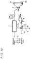
- the distance from an electron gun 6b to the screen 6a is the shortest at the center of the screen 6a, longer at the top and bottom of the screen 6a, and the longest at the corners of the screen 6a. Consequently, a so-called horizontal pin is generated as illustrated in FIGURE 13(a). If this horizontal pin is left as it is, the displayed image appears distorted. Thus, usually a circuit is added to the horizontal deflection circuit for correcting this horizontal pin distortion.
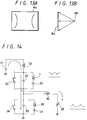
- FIGURE 14 shows the principle of a horizontal deflection circuit which is disclosed in Japanese Patent Publication Gazette No. 57-39102.
- a DC voltage from a power supply 31 is supplied through a coil 32 to a parallel circuit of a switch 33, the capacitor 24 and a series circuit of the horizontal deflection coil 7 and the capacitor 25.
- the power supply 31 and the coil 32 correspond to the power supply 3 and the primary winding 2a of the flyback transformer 2 in FIGURE 11.
- the switch 33 corresponds to the parallel circuit of the NPN transistor 22 and the diode 23.
- the parallel circuit (the first parallel circuit) of the switch 33, the capacitor 24 and the series circuit of the horizontal deflection coil 7 and the capacitor 25 is connected to a parallel circuit (the second parallel circuit) of a switch 34, a capacitor 35 and a series circuit of a coil 36 and a capacitor 37. Also, this second parallel circuit is connected in parallel to a series circuit of a coil 38 and a power supply 39. In other words, this horizontal deflection circuit is formed by connecting the first parallel circuit to the second parallel circuit having the same construction as the first parallel circuit.
- the retrace pulse (the voltage V24 across the capacitor 24), as shown in FIGURE 15(a), supplied to the horizontal deflection coil 7, be adjusted in its level to be larger at substantially the central portion (at the central area of the screen) than at the left and right ends (at the upper and lower ends of the screen).
- the level of a retrace pulse resulting from the addition of this voltage V24 and the voltage, V35 across the capacitor 35 is constant as shown in FIGURE 15(c) because it is specified by the power supply 31 and the width of the retrace pulse.
- the voltage level V24 can be adjusted to be larger at substantially the central portion (at the central region of the screen) than at the left and right ends (at the upper and lower ends of the screen).
- the switch 34 is operated to switch in synchronism with the switch 33, so that the retrace pulse is generated at the junction between the capacitor 35 and the coil 38.
- the voltage from the power supply 39 is changed to decrease at the central portion (at the central region of the screen) and increase at the left and right ends (at the upper and lower ends of the screen) in association with the vertical deflection period as shown in FIGURE 15(b).
- the level of voltage V24 as shown in FIGURE 15(a), is changed to be larger at substantially the central portion (at the central region of the screen) than at the left and right ends (at the upper and lower ends of the screen), so that the horizontal pin is corrected.
- the power supply modulating system modulates the voltage of the power supply 3 by the vertical deflection period as, for example, shown in FIGURE 11.
- the transformer has its secondary winding connected in series with the horizontal deflection coil 7, and its primary winding supplied with a vertical deflection current.
- FIGURE 14 can be used not only for the separate type arrangement but also for the conventional type horizontal deflection circuit.
- the various voltages derived from the secondary winding of the transformer, even with the coil 32 connected as its primary winding, are not modulated by the vertical deflection period.
- the present invention also provides reduced current drain.
- a deflection current circuit having reduced power requirements is provided.
- a switch 33 is controlled by a control circuit 71 in association with the horizontal deflection period.
- a switch 73 is controlled by the control circuit 72 in synchronization with the horizontal deflection period modulated by the vertical deflection period.
- Switch 33 is turned off in the retrace interval, and during the period in which the switch 33 is in the off-state, the switch 73 is turned off for a predetermined period.
- the off-period of the switch 73 is modulated by the vertical deflection period to produce greater horizontal deflection in the center of the screen.
- the deflection current generating circuit of the present invention has a switch 33 as a first switching element for performing a switching operation in association with the horizontal deflection period as described above.
- a coil 32 acts as a retrace pulse generating coil for generating a retrace pulse in association with the switching operation of the switch 33.
- a horizontal deflection coil 7 and capacitors 24, 25 form resonant circuits for resonating in association with the switching operation of the switch 33.
- a switch 73 serves as a second switching element and switches in association with both the horizontal deflection period and the vertical deflection period.
- a capacitor 74 serves as an "adjust pulse" generator acting in conjunction with the operation of the switch 73.
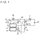
- FIGURE 1 is a circuit diagram of the construction of one embodiment of the deflection current generating circuit of the invention.
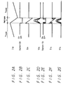
- FIGURE 2 is a timing chart for the operation of the embodiment of FIGURE 1.
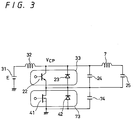
- FIGURE 3 is a circuit diagram of the construction of a second embodiment of the deflection current generating circuit of the invention.
- FIGURE 4 is a timing chart for the embodiment of FIGURE 3.
- FIGURE 5 is a circuit diagram of the construction of the transformer which can be used in the embodiments of FIGURES 1 and 3.
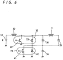
- FIGURE 6 is circuit diagram of the construction of a third embodiment of the deflection current generating circuit of the invention.
- FIGURE 7 is a timing chart for the operation in the case of change of DC component of the current I32 in the embodiments of FIGURES 1, 3 and 6.
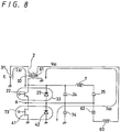
- FIGURE 8 is a circuit diagram of the construction of a fourth embodiment of the deflection current generating circuit of the invention.
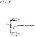
- FIGURE 9 is a diagram for the operation of the coil 63 in the embodiment of FIGURE 8.
- FIGURE 10 is a block diagram of an example of the construction of the conventional horizontal deflection circuit.
- FIGURE 11 is a circuit diagram of an example of the construction of the horizontal deflection circuit 1 in the example of FIGURE 10.
- FIGURE 12 is a timing chart for the operation of the construction of FIGURE 11.
- FIGURE 13 is a diagram to which reference is made in explaining the principle of the generation of the horizontal pin in the example of FIGURE 11.
- FIGURE 14 is a circuit diagram of the construction of an example of the conventional deflection current generating circuit for correcting the horizontal pin.
- FIGURE 15 is a wave form diagram to which reference is made in explaining the operating of the example of FIGURE 14.
- FIGURE 1 is a circuit diagram of one embodiment of the deflection current generating circuit of the invention. Like elements corresponding to those in FIGURES 10, 11 and 14 are identified by the same reference numerals.
- a parallel circuit of a switch 73 and a capacitor 74 is connected in a series with a parallel circuit of the switch 33, the capacitor 24 and a series circuit of the horizontal deflection coil 7 and the capacitor 25.
- the switch 33 is controlled by a control circuit 71 so as to switch in synchronization with the horizontal deflection period.
- the switch 33 is switched off during the horizontal retrace period and is on otherwise.
- Switch 73 is also on during the trace period.
- Switch 73 is off during at least a portion of the retrace period.
- the pulse width of the off time of switch 73 is modulated by the vertical period as will be explained later in greater detail.
- FIGURE 3 shows an embodiment of the invention of FIGURE 1 in which diodes and transistors serve as the switches 33 and 73.
- the switches 33 and 73 are respectively implemented using the NPN transistor 22 and the diode 23, and the FET 41 and the diode 42 or an FET.
- the capacitor 74 is connected in parallel with the switch 73.
- the switches 33 and 73 are turned off in the retrace interval of the horizontal deflection interval, and turned on in the trace interval.
- the switch 73 is turned off during a predetermined portion of the period in which the switch 33 is in the off-state.
- the off-period of the switch 73 is modulated in accordance with the vertical deflection period so that the duration of time in which switch 73 is off varies depending upon the vertical deflection period. That is, the switch 73 is off for a shorter time period near the center of the vertical deflection period (center of the screen), and off for a longer time period near the beginning and end of the vertical deflection period (top and bottom of the screen).
- the pulse width of the off time for the switch 73 is modulated in accordance with the vertical deflection period so that the pulse width is shortest in the center of the vertical period and longest near the top and bottom of the trace. This causes current in the horizontal deflection coil to be greater near the center of the screen than at the upper and lower ends of the screen as required to correct horizontal pin.
- control signal for switch 73 can be a pulse width modulated horizontal synchronization pulse wherein the modulating signal has a period equal to the vertical deflection period.
- control signal used to control switch 73 may use digital techniques to modulate the horizontal synchronization pulse by the vertical deflection period to achieve a pulse width modulated signal.
- the width of the pulse can be varied on a line by line basis in descrete increments on the basis of the line count. That is, the line count can be used to determine the width of the off time pulse of switch 73 and thus determine the amount of pin correction.
- the switch 73 is caused to switch in synchronization with the horizontal deflection period as in FIGURE 2e.
- This switching operation itself is modulated by the vertical deflection period so that an adjustment signal across capacitor 74 is adjusted in its level.
- the horizontal pin is corrected and the power consumption is reduced as compared with the case of adjusting the power supply voltage itself for setting the level of the adjust pulse.
- the switch 33 is controlled by the control circuit 71 so that it is turned on during the trace interval for the horizontal deflection and turned off during the retrace interval (FIGURE 2(b)).
- the saw-tooth wave current I32 (FIGURE 2(a)) flowing in the coil 32 flows through the switch 33 when the switch 33 is in the on-state, but flows through the capacitor 24 when the switch 33 is in the off-state.
- the switch 73 is controlled by the control circuit 72 so that it is turned off for a predetermined time during the retrace interval in which the switch 33 is in the off-state (FIGURE 2(c)).
- the current I32 flows in the switches 33 and 73 when the switches 33 and 73 are in the on-state, but flows in the capacitors 24 and 74 when the switches 33 and 73 are in the off-state.
- the switch 33 is in the off-state but the switch 73 is in the on-state, the current flows in the capacitor 24 and the switch 73.
- the saw-tooth wave current I flows in the resonant circuit of the horizontal deflection coil 7 and capacitors 25 and 24.
- the capacitance of the capacitor 24 is selected to be much smaller than that of the capacitor 74. Therefore, the retrace period (time) Tr is substantially determined by the capacitance values of the capacitors 24 and 25 and the inductance of the horizontal deflection coil 7. It is approximately the same when the capacitor 74 is connected as when this capacitor 74 is not connected since the series combination of capacitors 74 and 24 is only slightly less than the capacitance of capacitor 24.
- Vcp V24+V74 (2)
- the energy for deflection, when the capacitor 74 is not connected, is given as (1/2)C24Vcp2 but, when the capacitor 74 is connected as shown in FIGURE 1, it is given as (1/2)C24V242 .
- the deflection current I7 is smaller when the capacitor 74 is connected (that is when switch 73 is off) than when it is not connected (switch 73 is on).
- the period in which the switch 73 is in the off-state (the period in which it is in the on-state) is modulated to vary the voltage V74, the voltage V24, and thus the deflection current I7, can be adjusted.
- the raster size can be controlled.
- the period in which the switch 73 is turned off is modulated by the vertical deflection period, the left and right pins can be corrected.
- the resultant current I24 (FIGURE 2(c)) of the currents I32 and I7 flows in the capacitor 24. Since both the currents I32 and I7 are saw-tooth waves, the current I24 is as shown in FIGURE 2(c)). If the switch 73 is turned on and off just in synchronism with the switch 33, the current I32 flows through the switch 73 or capacitor 74 to the ground, and thus the I74 equals to the current flowing in the capacitor 24 in the interval in which the switch 33 (or 73) is in the off-state.
- the off-timing (FIGURE 2(c)) of the switch 73 is modulated so that the off-time pulse is narrower than the off-time pulse (FIGURE 2(b)) of the switch 33. Then, in the interval in which the switch 33 is off and the switch 73 is on, the current I32 flows in the switch 73, but in the interval in which both switches 33 and 73 are off, the current flows in the capacitors 24 and 74. Therefore, the current I74 has a waveform (the waveform of current I32 cut out) as indicated by the solid line in FIGURE 2(f).
- the interval in which the current I32 is cut out can be changed and adjusted by Vcp at the junction between the coil 32 and the horizontal deflection yoke 7 as shown in FIGURE 4(b) is the sum of the voltage V74 across the capacitor 74 shown in FIGURE 4(d) and the voltage V24 across the capacitor 24 shown in FIGURE 4(c).
- the frequency (width) and height of the voltage V74 developed across the capacitor 74 can be controlled.
- the increase of the frequency means that the width of the pulse shown in FIGURE 4(d) is decreased, and the decrease of the frequency means that the width of the pulse is increased.
- the coil 32 shown in FIGURES 1 and 3 can be the primary coil of the flyback transformer 2 as shown in FIGURE 5.
- the transformer has secondary coils 51 and 54.
- the output of the secondary coil 51 is rectified by a diode 52, and divided by a resistor 53 to produce a focus voltage.
- the secondary coil 54 produces output pulses of opposite polarities.
- FIGURE 6 shows a third embodiment.
- the emitter of the NPN transistor 22, which is also used in the embodiment shown in FIGURE 3 is grounded.
- the other portions are the same as in FIGURE 3. This arrangement operates in essentially the same manner as the embodiment of FIGURE 3.
- FIGURE 8 shows another embodiment which can be used for the conventional type circuit arrangement.
- the transformer 2 has a first coil formed of the coil 32 and a secondary coil 61.
- the secondary coil 61 is connected through a series circuit of a coil 63 and a capacitor 62 to the junction between a capacitor 74 and the capacitor 25.
- the other portions are constructed in the same way as in the embodiments shown in FIGURES 1 and 3. That is, in this embodiment, a main resonant circuit formed of the horizontal deflection coil 7 and the capacitors 25 and 24 is connected with a sub-resonant circuit formed of the secondary coil 61, the coil 63, the capacitor 62 and the capacitor 74.
- the transformer 2 is the flyback transformer.
- the inductance of the secondary winding 61 of the flyback transformer should be made much larger than that of the coil 63 of the sub-resonant circuit.
- the resonant frequency of the main resonant circuit is specified by the inductance L7 of the horizontal deflection coil 7 and the static capacitance C25 of the capacitor 25. In the retrace interval, it is specified by the inductance L7, the static capacitance C25 and the static capacitance C24 of the capacitor 24. In the trace interval, the frequency of the sub-resonant circuit is specified by the static capacitance C62 of the capacitor 62 and the inductance M63 (which will be described later) of the coil 63. In the retrace interval, it is specified by the inductance M63, the static capacitance C62 and the static capacitance C74 of the capacitor 74 (see Table 1). TABLE 1 Trace Interval Retrace Interval Main resonant circuit L7, C25 L7, C25, C24 Sub-resonant circuit M63, C62 M63, C62, C74
- the frequency f T in the trace interval should be set to be much smaller in value than the frequency f R in the retrace interval.
- the trace interval of time should be a much longer value than the retrace interval of time.
- the capacitance C62 is selected to have a much larger value than the capacitance value C74.
- the voltage V74 across the capacitor 74 and the output voltage V61 induced in the secondary coil 61 of the transformer 2 are supplied to one terminal of the coil 63 and to the other terminal thereof, respectively.
- the imaginary ground point of the coil 63 is moved in accordance with the voltage values of the voltages V74 and V61.
- the M63(L63) Since the frequency is determined by the product of M63(L63) and C74, the M63(L63) should be selected to be much larger than C74.
- the inductance L61 of the secondary coil 61 should be set to be much larger than the inductance value L63 of the coil 63.
- the current I63 flows as a bias from the secondary coil 61 of the transformer 2 through the coil 63 and the capacitor 62 to the capacitor 74, the resultant current of I32 and I63 flows in the capacitor 74 in the stationary state.
- the current I63 is set to be much larger than current I32, the amount of change of current flowing in the capacitor 74 is relatively small even though the current I32 is changed with the change of the applied high voltage in the secondary winding of the transformer 2. Therefore, a flyback transformer can be used for the transformer 2, and thus this circuit arrangement can be applied to the so-called conventional type circuit arrangement.
- the capacitor 62 in FIGURE 8 can be connected between the capacitor 25 and the capacitor 74 so as to be common to the main resonant circuit and the sub-resonant circuit.
- the emitter of the NPN transistor 22 can be grounded as in FIGURE 6.
- the switch 33 is implemented using the NPN transistor 22 and the diode 23 and the switch 73 is formed of the FET 41 and the diode 42
- the switch 33 may be formed of an FET and a diode
- the switch 73 may be formed of a transistor and a diode.
- both the switches 33 and 73 can be formed of a transistor and a diode, or of an FET and a diode.
- the parasitic diode can be substituted for the discrete diode.
- use of an FET makes the circuit simpler, and the switching speed higher, than use of a transistor.
- Other switch arrangements will occur to those skilled in the art.
- the second switching element is not only switched in association with the horizontal deflection period, but also modulated with the vertical deflection period, the horizontal pin can be corrected. Moreover, since the level of the adjust pulse is adjusted by controlling the switching itself without adjusting the power supply voltage, the power consumption can be reduced.
- the second switching element since the second switching element performs a complete switching operation, the loss is small. Since the switching is performed within the retrace interval, noise is suppressed from being visible.
- the DC or AC controllable range (dynamic range) of the horizontal deflection current can be widened. Since the height of the flyback pulse is not changed by AC control of the horizontal deflection current, this pulse makes it possible to stably produce various voltages.
- the retrace pulse generation coil can be formed of a transformer, and in this case the output of the secondary winding of the transformer can be supplied to the adjust pulse generation circuit.
- this circuit arrangement can be used in the horizontal deflection circuit of the conventional type.
Abstract
Description
- This invention relates generally to the field of deflection current generating circuits suitable for use in, for example, a television receiver or a video monitor. More particularly, this invention relates to a television deflection circuit having horizontal pin distortion compensation and reduced power consumption.
- A conventional arrangement of a horizontal deflection circuit and neighboring circuits of a television receiver are shown in FIGURE 10. A
horizontal deflection circuit 1 is connected with a power supply 3 through aprimary coil 2a of aflyback transformer 2. Asecondary winding 2b of thetransformer 2 is connected to a rectifying/smoothing circuit which is formed of adiode 4 and acapacitor 5. A horizontal deflection current from thehorizontal deflection circuit 1 is supplied to adeflection yoke 7 of aCRT 6 having ascreen 6a. - FIGURE 11 shows the circuit arrangement of the
horizontal deflection circuit 1. Thishorizontal deflection circuit 1 has a parallel circuit of anNPN transistor 22, adiode 23, and acapacitor 24 all in parallel with the series combination ofdeflection yoke 7 andcapacitor 25. Thetransformer 2 also has asecondary winding 2c, the output of which is rectified by adiode 21. - The operation of this arrangement will be described below. The DC voltage from the power supply 3 is supplied through the
primary coil 2a of thetransformer 2 to the collector of theNPN transistor 22. ThisNPN transistor 22 is turned on and off when a signal having a period corresponding to the horizontal deflection period is supplied to its base. The result is that theNPN transistor 22 produces, at its collector, a flyback pulse (retrace pulse) Vcp as shown in FIGURE 12(b). - The
capacitors deflection yoke 7 make up a resonant circuit, which is resonant at the switching frequency of theNPN transistor 22. Thus, in the deflection yoke 7 a deflection current I₇ of a so-called saw-tooth wave flows. As shown in FIGURE 12(a), this wave linearly increases during the trace interval and linearly decreases during the retrace interval. The electron beam scans (or is deflected) in the horizontal direction on thescreen 6a of theCRT 6 under control of this deflection current. - The flyback pulse voltage Vcp is boosted by the
secondary coil 2c of theflyback transformer 2, and rectified by thediode 21 so that a high voltage Hv is generated at the cathode of the diode. This high voltage Hv is supplied to the anode of theCRT 6. The voltage induced in thesecondary coil 2b is rectified bydiode 4 and smoothed bycapacitor 5 into a DC voltage Vc. This voltage Vc is used for the focus voltage and heater voltage of theCRT 6 and so on. - As shown in FIGURE 12(b), the distance from an
electron gun 6b to thescreen 6a is the shortest at the center of thescreen 6a, longer at the top and bottom of thescreen 6a, and the longest at the corners of thescreen 6a. Consequently, a so-called horizontal pin is generated as illustrated in FIGURE 13(a). If this horizontal pin is left as it is, the displayed image appears distorted. Thus, usually a circuit is added to the horizontal deflection circuit for correcting this horizontal pin distortion. - FIGURE 14 shows the principle of a horizontal deflection circuit which is disclosed in Japanese Patent Publication Gazette No. 57-39102. In this example, a DC voltage from a
power supply 31 is supplied through acoil 32 to a parallel circuit of aswitch 33, thecapacitor 24 and a series circuit of thehorizontal deflection coil 7 and thecapacitor 25. Thepower supply 31 and thecoil 32 correspond to the power supply 3 and theprimary winding 2a of theflyback transformer 2 in FIGURE 11. Theswitch 33 corresponds to the parallel circuit of theNPN transistor 22 and thediode 23. - In this embodiment, the parallel circuit (the first parallel circuit) of the
switch 33, thecapacitor 24 and the series circuit of thehorizontal deflection coil 7 and thecapacitor 25 is connected to a parallel circuit (the second parallel circuit) of aswitch 34, acapacitor 35 and a series circuit of acoil 36 and acapacitor 37. Also, this second parallel circuit is connected in parallel to a series circuit of a coil 38 and apower supply 39. In other words, this horizontal deflection circuit is formed by connecting the first parallel circuit to the second parallel circuit having the same construction as the first parallel circuit. - In order to correct the horizontal pin, it is necessary that the retrace pulse (the voltage V₂₄ across the capacitor 24), as shown in FIGURE 15(a), supplied to the
horizontal deflection coil 7, be adjusted in its level to be larger at substantially the central portion (at the central area of the screen) than at the left and right ends (at the upper and lower ends of the screen). The level of a retrace pulse resulting from the addition of this voltage V₂₄ and the voltage, V₃₅ across thecapacitor 35 is constant as shown in FIGURE 15(c) because it is specified by thepower supply 31 and the width of the retrace pulse. - Thus, if the voltage V₃₅ is changed to decrease at the central portion (at the central region of the screen) and increase at the left and right ends (at the upper and lower ends of the screen) in association with the vertical deflection period as shown in FIGURE 15(b), the voltage level V₂₄ can be adjusted to be larger at substantially the central portion (at the central region of the screen) than at the left and right ends (at the upper and lower ends of the screen).
- In this example, the
switch 34 is operated to switch in synchronism with theswitch 33, so that the retrace pulse is generated at the junction between thecapacitor 35 and the coil 38. In addition, the voltage from thepower supply 39 is changed to decrease at the central portion (at the central region of the screen) and increase at the left and right ends (at the upper and lower ends of the screen) in association with the vertical deflection period as shown in FIGURE 15(b). As a result, the level of voltage V₂₄, as shown in FIGURE 15(a), is changed to be larger at substantially the central portion (at the central region of the screen) than at the left and right ends (at the upper and lower ends of the screen), so that the horizontal pin is corrected. - Other known horizontal pin correction systems are known as the power supply modulating system and the PCT system. The power supply modulating system modulates the voltage of the power supply 3 by the vertical deflection period as, for example, shown in FIGURE 11. In the PCT system, as shown in FIGURE 11, the transformer has its secondary winding connected in series with the
horizontal deflection coil 7, and its primary winding supplied with a vertical deflection current. - In either of these systems, however, the voltage Vcp is modulated by the vertical deflection period, and hence the various voltages taken out of the
transformer 2 are modulated by the vertical deflection period. Therefore, these systems can be applied to the so-called separate type circuit arrangement having the horizontal deflection circuit and the high voltage generating circuit separately provided, but cannot be used in the so-called conventional type circuit arrangement having both circuits combined into a single circuit. - The system shown in FIGURE 14 can be used not only for the separate type arrangement but also for the conventional type horizontal deflection circuit. In FIGURE 14, the various voltages derived from the secondary winding of the transformer, even with the
coil 32 connected as its primary winding, are not modulated by the vertical deflection period. - Several significant problems exist with these known circuit arrangements. In the circuit arrangement shown in FIGURE 14, it is necessary for current to flow not only in the second parallel circuit of the
switch 34, thecapacitor 35 and the series circuit of thecoil 36 and thecapacitor 37, but also in the series circuit of the coil 38 and thepower supply 39, and thus the power consumption is relatively large. The present invention reduces horizontal pin distortion at a significantly reduced power consumption. - It is an object of the present invention to provide an improved deflection current generating circuit for use in a television or video monitor.
- It is a feature that the present invention to provides improvement in horizontal pin distortion.
- It is an advantage that the present invention also provides reduced current drain.
- These and other objects, advantages and features of the invention will become apparent to those skilled in the art upon consideration of the following description of the invention.
- In one embodiment of the present invention, a deflection current circuit having reduced power requirements is provided. A
switch 33 is controlled by acontrol circuit 71 in association with the horizontal deflection period. Aswitch 73 is controlled by thecontrol circuit 72 in synchronization with the horizontal deflection period modulated by the vertical deflection period.Switch 33 is turned off in the retrace interval, and during the period in which theswitch 33 is in the off-state, theswitch 73 is turned off for a predetermined period. The off-period of theswitch 73 is modulated by the vertical deflection period to produce greater horizontal deflection in the center of the screen. - The deflection current generating circuit of the present invention has a
switch 33 as a first switching element for performing a switching operation in association with the horizontal deflection period as described above. Acoil 32 acts as a retrace pulse generating coil for generating a retrace pulse in association with the switching operation of theswitch 33. Ahorizontal deflection coil 7 andcapacitors switch 33. Aswitch 73 serves as a second switching element and switches in association with both the horizontal deflection period and the vertical deflection period. Acapacitor 74 serves as an "adjust pulse" generator acting in conjunction with the operation of theswitch 73. - The features of the invention believed to be novel are set forth with particularity in the appended claims. The invention itself however, both as to organization and method of operation, together with further objects and advantages thereof, may be best understood by reference to the following description taken in conjunction with the accompanying drawing.
- FIGURE 1 is a circuit diagram of the construction of one embodiment of the deflection current generating circuit of the invention.
- FIGURE 2 is a timing chart for the operation of the embodiment of FIGURE 1.
- FIGURE 3 is a circuit diagram of the construction of a second embodiment of the deflection current generating circuit of the invention.
- FIGURE 4 is a timing chart for the embodiment of FIGURE 3.
- FIGURE 5 is a circuit diagram of the construction of the transformer which can be used in the embodiments of FIGURES 1 and 3.
- FIGURE 6 is circuit diagram of the construction of a third embodiment of the deflection current generating circuit of the invention.
- FIGURE 7 is a timing chart for the operation in the case of change of DC component of the current I₃₂ in the embodiments of FIGURES 1, 3 and 6.
- FIGURE 8 is a circuit diagram of the construction of a fourth embodiment of the deflection current generating circuit of the invention.
- FIGURE 9 is a diagram for the operation of the
coil 63 in the embodiment of FIGURE 8. - FIGURE 10 is a block diagram of an example of the construction of the conventional horizontal deflection circuit.
- FIGURE 11 is a circuit diagram of an example of the construction of the
horizontal deflection circuit 1 in the example of FIGURE 10. - FIGURE 12 is a timing chart for the operation of the construction of FIGURE 11.
- FIGURE 13 is a diagram to which reference is made in explaining the principle of the generation of the horizontal pin in the example of FIGURE 11.
- FIGURE 14 is a circuit diagram of the construction of an example of the conventional deflection current generating circuit for correcting the horizontal pin.
- FIGURE 15 is a wave form diagram to which reference is made in explaining the operating of the example of FIGURE 14.
- FIGURE 1 is a circuit diagram of one embodiment of the deflection current generating circuit of the invention. Like elements corresponding to those in FIGURES 10, 11 and 14 are identified by the same reference numerals. In this embodiment, a parallel circuit of a
switch 73 and acapacitor 74 is connected in a series with a parallel circuit of theswitch 33, thecapacitor 24 and a series circuit of thehorizontal deflection coil 7 and thecapacitor 25. Theswitch 33 is controlled by acontrol circuit 71 so as to switch in synchronization with the horizontal deflection period. - Referring briefly to FIGURE 2, and in particular FIGURE 2b, the
switch 33 is switched off during the horizontal retrace period and is on otherwise.Switch 73 is also on during the trace period.Switch 73 is off during at least a portion of the retrace period. In order to provide the pin correction, the pulse width of the off time ofswitch 73 is modulated by the vertical period as will be explained later in greater detail. - FIGURE 3 shows an embodiment of the invention of FIGURE 1 in which diodes and transistors serve as the
switches switches NPN transistor 22 and thediode 23, and theFET 41 and thediode 42 or an FET. Thecapacitor 74 is connected in parallel with theswitch 73. - As illustrated in FIGURE 2, the
switches switch 73 is turned off during a predetermined portion of the period in which theswitch 33 is in the off-state. The off-period of theswitch 73 is modulated in accordance with the vertical deflection period so that the duration of time in which switch 73 is off varies depending upon the vertical deflection period. That is, theswitch 73 is off for a shorter time period near the center of the vertical deflection period (center of the screen), and off for a longer time period near the beginning and end of the vertical deflection period (top and bottom of the screen). In other words, the pulse width of the off time for theswitch 73 is modulated in accordance with the vertical deflection period so that the pulse width is shortest in the center of the vertical period and longest near the top and bottom of the trace. This causes current in the horizontal deflection coil to be greater near the center of the screen than at the upper and lower ends of the screen as required to correct horizontal pin. - When the off time of
switch 33 and switch 73 are identical, no pin correction is introduced. The shorter the off time ofswitch 73 is made, the more pin correction is introduced. Thus the control signal forswitch 73 can be a pulse width modulated horizontal synchronization pulse wherein the modulating signal has a period equal to the vertical deflection period. - In one embodiment, the control signal used to control
switch 73 may use digital techniques to modulate the horizontal synchronization pulse by the vertical deflection period to achieve a pulse width modulated signal. Thus, the width of the pulse can be varied on a line by line basis in descrete increments on the basis of the line count. That is, the line count can be used to determine the width of the off time pulse ofswitch 73 and thus determine the amount of pin correction. - According to the deflection current generating circuit of the above construction, the
switch 73 is caused to switch in synchronization with the horizontal deflection period as in FIGURE 2e. This switching operation itself is modulated by the vertical deflection period so that an adjustment signal acrosscapacitor 74 is adjusted in its level. Thus, the horizontal pin is corrected and the power consumption is reduced as compared with the case of adjusting the power supply voltage itself for setting the level of the adjust pulse. - The
switch 33 is controlled by thecontrol circuit 71 so that it is turned on during the trace interval for the horizontal deflection and turned off during the retrace interval (FIGURE 2(b)). The saw-tooth wave current I₃₂ (FIGURE 2(a)) flowing in thecoil 32 flows through theswitch 33 when theswitch 33 is in the on-state, but flows through thecapacitor 24 when theswitch 33 is in the off-state. Theswitch 73 is controlled by thecontrol circuit 72 so that it is turned off for a predetermined time during the retrace interval in which theswitch 33 is in the off-state (FIGURE 2(c)). - The current I₃₂ flows in the
switches switches capacitors switches switch 33 is in the off-state but theswitch 73 is in the on-state, the current flows in thecapacitor 24 and theswitch 73. When theswitch 33 is in the off-state, the saw-tooth wave current I flows in the resonant circuit of thehorizontal deflection coil 7 andcapacitors - The capacitance of the
capacitor 24 is selected to be much smaller than that of thecapacitor 74. Therefore, the retrace period (time) Tr is substantially determined by the capacitance values of thecapacitors horizontal deflection coil 7. It is approximately the same when thecapacitor 74 is connected as when thiscapacitor 74 is not connected since the series combination ofcapacitors capacitor 24. The voltage Vcp between the ground potential and the junction of thecoil 32 and thehorizontal deflection coil 7 is given by the following equation:

This voltage Vcp is equal to the sum of the voltage V₂₄ across thecapacitor 24 and the voltage V₇₄ across thecapacitor 74. That is, the following equation is satisfied:

The energy for deflection, when thecapacitor 74 is not connected, is given as
capacitor 74 is connected as shown in FIGURE 1, it is given as
capacitor 74 is connected (that is whenswitch 73 is off) than when it is not connected (switch 73 is on). Thus, if the period in which theswitch 73 is in the off-state (the period in which it is in the on-state) is modulated to vary the voltage V₇₄, the voltage V₂₄, and thus the deflection current I₇, can be adjusted. The result is that the raster size can be controlled. In addition, if the period in which theswitch 73 is turned off is modulated by the vertical deflection period, the left and right pins can be corrected. - In the retrace interval in which the
switch 33 is in the off-state, the resultant current I₂₄ (FIGURE 2(c)) of the currents I₃₂ and I₇ flows in thecapacitor 24. Since both the currents I₃₂ and I₇ are saw-tooth waves, the current I₂₄ is as shown in FIGURE 2(c)). If theswitch 73 is turned on and off just in synchronism with theswitch 33, the current I₃₂ flows through theswitch 73 orcapacitor 74 to the ground, and thus the I₇₄ equals to the current flowing in thecapacitor 24 in the interval in which the switch 33 (or 73) is in the off-state. - Now consider that the off-timing (FIGURE 2(c)) of the
switch 73 is modulated so that the off-time pulse is narrower than the off-time pulse (FIGURE 2(b)) of theswitch 33. Then, in the interval in which theswitch 33 is off and theswitch 73 is on, the current I₃₂ flows in theswitch 73, but in the interval in which bothswitches capacitors coil 32 and thehorizontal deflection yoke 7 as shown in FIGURE 4(b) is the sum of the voltage V₇₄ across thecapacitor 74 shown in FIGURE 4(d) and the voltage V₂₄ across thecapacitor 24 shown in FIGURE 4(c). Thus, if the off-timing of theFET 41 is adjusted in association with the vertical deflection period, the frequency (width) and height of the voltage V₇₄ developed across thecapacitor 74 can be controlled. The increase of the frequency means that the width of the pulse shown in FIGURE 4(d) is decreased, and the decrease of the frequency means that the width of the pulse is increased. If the pulse width is decreased, the pulse height is decreased, while if the width is increased, the pulse height is increased. As a result, the voltage Vcp (constant) minus the voltage V₇₄, or the voltage V₂₄ is changed as shown in FIGURE 4(e). - Although only the off-period of the
NPN transistor 22 andFET 41 is shown in FIGURE 4, the on-periods of thediodes NPN transistor 22 and thediode 23 are replaced by thesingle switch 33 and when theFET 41 and thediode 42 are replaced by thesingle switch 73, the operation is the same as in FIGURE 2. - The
coil 32 shown in FIGURES 1 and 3 can be the primary coil of theflyback transformer 2 as shown in FIGURE 5. In this case, the transformer hassecondary coils secondary coil 51 is rectified by adiode 52, and divided by aresistor 53 to produce a focus voltage. Thesecondary coil 54 produces output pulses of opposite polarities. - FIGURE 6 shows a third embodiment. In this embodiment, the emitter of the
NPN transistor 22, which is also used in the embodiment shown in FIGURE 3, is grounded. The other portions are the same as in FIGURE 3. This arrangement operates in essentially the same manner as the embodiment of FIGURE 3. - In the embodiments shown in FIGURES 1, 3 and 6, when the DC component of the current I₃₂ flowing in the
coil 32 is changed as, for example, shown in FIGURE 7(a), thecurrent I₇ ₄ as shown in FIGURE 7(c) flows in thecapacitor 74 in accordance with the switching operation of theswitch 73 shown in FIGURE 7(b). In other words, in the DC component superimposed state (shown on the right hand of FIGURE 7), the current I₇₄ is changed into a nonlinear shape, and the voltage V₇₄ across thecapacitor 74 is changed as shown in FIGURE 7(d). This means that when the current I₃₂ flowing in thecoil 32 is changed, the raster size is changed. Thus, this invention can be applied to the so-called separate type circuit arrangement having the horizontal deflection circuit and the high voltage generating circuit separately provided, but cannot be applied to the conventional type circuit arrangement having both circuits combined. - FIGURE 8 shows another embodiment which can be used for the conventional type circuit arrangement. In this embodiment, the
transformer 2 has a first coil formed of thecoil 32 and asecondary coil 61. Thesecondary coil 61 is connected through a series circuit of acoil 63 and acapacitor 62 to the junction between acapacitor 74 and thecapacitor 25. The other portions are constructed in the same way as in the embodiments shown in FIGURES 1 and 3. That is, in this embodiment, a main resonant circuit formed of thehorizontal deflection coil 7 and thecapacitors secondary coil 61, thecoil 63, thecapacitor 62 and thecapacitor 74. Thetransformer 2 is the flyback transformer. The inductance of the secondary winding 61 of the flyback transformer should be made much larger than that of thecoil 63 of the sub-resonant circuit. - According to this arrangement, during the first half of the retrace interval, current flows in the path of
capacitor 74,capacitor 62,coil 63, andsecondary coil 61 oftransformer 2, while in the second half of the retrace interval, the current I₆₃ flows in thecoil 63 through the path in the opposite direction. - In the trace interval, the resonant frequency of the main resonant circuit is specified by the inductance L₇ of the
horizontal deflection coil 7 and the static capacitance C₂₅ of thecapacitor 25. In the retrace interval, it is specified by the inductance L₇, the static capacitance C₂₅ and the static capacitance C₂₄ of thecapacitor 24. In the trace interval, the frequency of the sub-resonant circuit is specified by the static capacitance C₆₂ of thecapacitor 62 and the inductance M₆₃ (which will be described later) of thecoil 63. In the retrace interval, it is specified by the inductance M₆₃, the static capacitance C₆₂ and the static capacitance C₇₄ of the capacitor 74 (see Table 1).TABLE 1 Trace Interval Retrace Interval Main resonant circuit L₇, C₂₅ L₇, C₂₅, C₂₄ Sub-resonant circuit M₆₃, C₆₂ M₆₃, C₆₂, C₇₄ - In the Main resonant circuit and the sub-resonant circuit, the frequency fT in the trace interval should be set to be much smaller in value than the frequency fR in the retrace interval. In other words, the trace interval of time should be a much longer value than the retrace interval of time. In order to realize this, the capacitance C₆₂ is selected to have a much larger value than the capacitance value C₇₄.
- The frequencies fT and fR are given by the following equations:


where Cφ is the combined series capacitance of thecapacitors

M₆₃ is not the original inductance L₆₃ of thecoil 63, but the equivalent inductance specified in accordance with the voltage developed thereacross. - In other words, as shown in FIGURE 9, the voltage V₇₄ across the
capacitor 74 and the output voltage V₆₁ induced in thesecondary coil 61 of thetransformer 2 are supplied to one terminal of thecoil 63 and to the other terminal thereof, respectively. As a result, the inductance M₆₃ contributing to the resonant operation of the sub-resonant circuit is expressed by the following equation:

The imaginary ground point of thecoil 63 is moved in accordance with the voltage values of the voltages V₇₄ and V₆₁. - Since fT is much smaller than fR the following inequality is satisfied.

The following inequality can be derived from the above inequality.

Rearranging the above inequality will yield the following inequality.

Where if
- Since the frequency is determined by the product of M₆₃(L₆₃) and C₇₄, the M₆₃(L₆₃) should be selected to be much larger than C₇₄.
- Since the
coil 61 serves to supply a predetermined bias to thecapacitor 74 through thecoil 63 and thecapacitor 62, the current flowing from thecoil 63 to thesecondary coil 61 of thetransformer 2 should be prevented from greatly affecting thetransformer 2. Thus, the inductance L₆₁ of thesecondary coil 61 should be set to be much larger than the inductance value L₆₃ of thecoil 63. - If the current I₆₃ flows as a bias from the
secondary coil 61 of thetransformer 2 through thecoil 63 and thecapacitor 62 to thecapacitor 74, the resultant current of I₃₂ and I₆₃ flows in thecapacitor 74 in the stationary state. Thus, if the current I₆₃ is set to be much larger than current I₃₂, the amount of change of current flowing in thecapacitor 74 is relatively small even though the current I₃₂ is changed with the change of the applied high voltage in the secondary winding of thetransformer 2. Therefore, a flyback transformer can be used for thetransformer 2, and thus this circuit arrangement can be applied to the so-called conventional type circuit arrangement. - The
capacitor 62 in FIGURE 8 can be connected between thecapacitor 25 and thecapacitor 74 so as to be common to the main resonant circuit and the sub-resonant circuit. The emitter of theNPN transistor 22 can be grounded as in FIGURE 6. - While in the above embodiment the
switch 33 is implemented using theNPN transistor 22 and thediode 23 and theswitch 73 is formed of theFET 41 and thediode 42, theswitch 33 may be formed of an FET and a diode, and theswitch 73 may be formed of a transistor and a diode. Also, both theswitches - Since the second switching element is not only switched in association with the horizontal deflection period, but also modulated with the vertical deflection period, the horizontal pin can be corrected. Moreover, since the level of the adjust pulse is adjusted by controlling the switching itself without adjusting the power supply voltage, the power consumption can be reduced.
- In addition, since the second switching element performs a complete switching operation, the loss is small. Since the switching is performed within the retrace interval, noise is suppressed from being visible. The DC or AC controllable range (dynamic range) of the horizontal deflection current can be widened. Since the height of the flyback pulse is not changed by AC control of the horizontal deflection current, this pulse makes it possible to stably produce various voltages.
- The retrace pulse generation coil can be formed of a transformer, and in this case the output of the secondary winding of the transformer can be supplied to the adjust pulse generation circuit. Thus, this circuit arrangement can be used in the horizontal deflection circuit of the conventional type.
- Thus it is apparent that in accordance with the present invention, an apparatus that fully satisfies the objectives, aims and advantages is set forth above. While the invention has been described in conjunction with specific embodiments, it is evident that many alternatives, modifications, permutations and variations will become apparent to those skilled in the art in light of the foregoing description. Accordingly, it is intended that the present invention embrace all such alternatives, modifications and variations as fall within the scope of the appended claims.
Claims (13)
- A deflection current generating circuit, comprising:
a first switching element (33) for switching in synchronization with a horizontal deflection period;
a retrace pulse generating coil (32) for generating a retrace pulse in association with the switching operation of said first switching element (33);
a resonant circuit (7,24,25) for resonating in association with the switching operation of said first switching element (33);
a second switching element (73) for switching in synchronization with both the horizontal deflection period and a vertical deflection period; and
an adjust pulse generating circuit (74), which is connected to said resonant circuit (7,24,25), for generating an adjust pulse in association with the switching operation of said second switching element (73). - A deflection current generating circuit according to claim 1, further comprising a transformer (2) which has a primary winding (32) and a secondary winding (61;51,54), and wherein said primary winding (32) includes said retrace pulse generating coil (32).
- A deflection current generating circuit according to claim 2, wherein a sub-resonant circuit (62,63) is connected between said secondary winding of said transformer (2) and said adjust pulse generating circuit (74).
- A deflection current generating circuit according to claim 3, wherein said sub-resonant circuit (62,63) includes a coil (63) and a capacitor (62) which resonate in association with the switching operation of said second switching element (73).
- A deflection current generating circuit according to claim 4, wherein said transformer (2) is a flyback transformer having at least one secondary winding (51) for generating a high voltage.
- A deflection current generating circuit according to claim 5, wherein said sub-resonant circuit (62,63) includes a coil (63); and wherein said secondary winding (61) of said flyback transformer (2) has a value of inductance which is much greater than an inductance of said coil (63) of said sub-resonant circuit (62,63).
- A deflection current generating circuit according to any one of claims 1 to 6, wherein said first and second switching elements (33,73) comprise a transistor (22) and a diode (23), and a FET (41) and a diode (42), respectively.
- A deflection current generating circuit according to claim 7, wherein said FET (41) and said diode (42) of said second switching element (73) comprise a FET having a parasitic diode.
- A deflection current generating circuit according to any one of claims 1 to 8, wherein said adjust pulse generating circuit (74) includes a capacitor (74) connected in parallel with said second switching element (73).
- A deflection current generating circuit according to any one of claims 1 to 9, wherein said first and second switching elements (33,73) are turned off in a retrace period and turned on in a trace period.
- A deflection current generating circuit according to claim 10, wherein said second switching element (73) is turned off only during a predetermined portion of the period in which said first switching element (33) is off.
- A deflection current generating circuit according to claim 11, wherein said off-period of said second switching (73) element is modulated by the vertical deflection period.
- A deflection current generating circuit, comprising in combination:
first switching means (33) for switching in synchronization with a horizontal synchronization pulse;
a retrace pulse generating coil (32), coupled to said first switching means (33), for generating a retrace pulse in response to said switching;
a resonant circuit (7,24,25) having a resonant frequency for resonating in response to said retrace pulse;
second switching means (73), coupled to said resonant circuit (7,24,25), and responsive to said horizontal synchronization pulse whose pulse width is modulated by a vertical deflection period, for applying an adjustment signal to said resonant circuit (7,24,25).
Applications Claiming Priority (3)
| Application Number | Priority Date | Filing Date | Title |
|---|---|---|---|
| JP3254490A JPH0568178A (en) | 1991-09-06 | 1991-09-06 | Deflected current generating circuit |
| JP25449091 | 1991-09-06 | ||
| JP254490/91 | 1991-09-06 |
Publications (3)
| Publication Number | Publication Date |
|---|---|
| EP0530809A1 true EP0530809A1 (en) | 1993-03-10 |
| EP0530809B1 EP0530809B1 (en) | 1997-07-09 |
| EP0530809B2 EP0530809B2 (en) | 2002-10-16 |
Family
ID=17265778
Family Applications (1)
| Application Number | Title | Priority Date | Filing Date |
|---|---|---|---|
| EP92115093A Expired - Lifetime EP0530809B2 (en) | 1991-09-06 | 1992-09-03 | Deflection current generating circuits |
Country Status (7)
| Country | Link |
|---|---|
| US (1) | US5285133A (en) |
| EP (1) | EP0530809B2 (en) |
| JP (1) | JPH0568178A (en) |
| KR (1) | KR930007209A (en) |
| DE (1) | DE69220737T3 (en) |
| ES (1) | ES2104781T5 (en) |
| MY (1) | MY108292A (en) |
Cited By (1)
| Publication number | Priority date | Publication date | Assignee | Title |
|---|---|---|---|---|
| EP1359669A1 (en) * | 2002-05-02 | 2003-11-05 | Deutsche Thomson-Brandt Gmbh | Driver circuit for driving a switching transistor |
Families Citing this family (4)
| Publication number | Priority date | Publication date | Assignee | Title |
|---|---|---|---|---|
| US5550442A (en) * | 1993-12-16 | 1996-08-27 | Matsushita Electric Industrial Co., Ltd. | Horizontal deflection circuit |
| JP3339294B2 (en) * | 1996-02-21 | 2002-10-28 | 日本ビクター株式会社 | Horizontal deflection high voltage generation circuit |
| KR100203404B1 (en) * | 1996-11-14 | 1999-06-15 | 윤종용 | Deflection driving circuit |
| JP3271581B2 (en) * | 1998-04-24 | 2002-04-02 | 株式会社村田製作所 | Deflection high voltage integrated power supply |
Citations (5)
| Publication number | Priority date | Publication date | Assignee | Title |
|---|---|---|---|---|
| US4169988A (en) * | 1977-07-25 | 1979-10-02 | Rca Corporation | Raster distortion correction circuit |
| US4242714A (en) * | 1978-03-27 | 1980-12-30 | Sony Corporation | Current control circuit |
| DE3234314C1 (en) * | 1982-09-16 | 1983-09-29 | Deutsche Thomson-Brandt Gmbh, 7730 Villingen-Schwenningen | Circuitry for correcting east-west pincushion distortion |
| EP0195392A2 (en) * | 1985-03-21 | 1986-09-24 | Nokia (Deutschland) GmbH | Horizontal deflection circuit |
| EP0332091A2 (en) * | 1988-03-10 | 1989-09-13 | Rca Licensing Corporation | Raster distortion corrected deflection circuit |
Family Cites Families (5)
| Publication number | Priority date | Publication date | Assignee | Title |
|---|---|---|---|---|
| JPS5419324A (en) * | 1977-07-14 | 1979-02-14 | Sony Corp | Current control circuit |
| JPS6024779A (en) * | 1983-07-20 | 1985-02-07 | Victor Co Of Japan Ltd | Saw tooth deflection current generating circuit |
| US4625155A (en) * | 1984-12-03 | 1986-11-25 | Rca Corporation | Resonant switching apparatus using a cascode arrangement |
| US4965496A (en) * | 1988-03-10 | 1990-10-23 | Rca Licensing Corporation | Protection arrangement of a deflection circuit |
| JPH02166970A (en) * | 1988-12-21 | 1990-06-27 | Hitachi Ltd | Horizontal deflection circuit |
-
1991
- 1991-09-06 JP JP3254490A patent/JPH0568178A/en not_active Withdrawn
-
1992
- 1992-09-02 KR KR1019920015883A patent/KR930007209A/en not_active Application Discontinuation
- 1992-09-03 DE DE69220737T patent/DE69220737T3/en not_active Expired - Fee Related
- 1992-09-03 US US07/939,797 patent/US5285133A/en not_active Expired - Lifetime
- 1992-09-03 MY MYPI92001576A patent/MY108292A/en unknown
- 1992-09-03 EP EP92115093A patent/EP0530809B2/en not_active Expired - Lifetime
- 1992-09-03 ES ES92115093T patent/ES2104781T5/en not_active Expired - Lifetime
Patent Citations (5)
| Publication number | Priority date | Publication date | Assignee | Title |
|---|---|---|---|---|
| US4169988A (en) * | 1977-07-25 | 1979-10-02 | Rca Corporation | Raster distortion correction circuit |
| US4242714A (en) * | 1978-03-27 | 1980-12-30 | Sony Corporation | Current control circuit |
| DE3234314C1 (en) * | 1982-09-16 | 1983-09-29 | Deutsche Thomson-Brandt Gmbh, 7730 Villingen-Schwenningen | Circuitry for correcting east-west pincushion distortion |
| EP0195392A2 (en) * | 1985-03-21 | 1986-09-24 | Nokia (Deutschland) GmbH | Horizontal deflection circuit |
| EP0332091A2 (en) * | 1988-03-10 | 1989-09-13 | Rca Licensing Corporation | Raster distortion corrected deflection circuit |
Non-Patent Citations (2)
| Title |
|---|
| PATENT ABSTRACTS OF JAPAN vol. 850, no. 618 (E-322)18 June 1985 & JP-A-60 024 779 ( NIPPON VICTOR KK ) 7 February 1985 * |
| PATENT ABSTRACTS OF JAPAN vol. 900, no. 917 (E-0979)17 September 1990 & JP-A-02 166 970 ( HITACHI LTD ) 27 June 1990 * |
Cited By (2)
| Publication number | Priority date | Publication date | Assignee | Title |
|---|---|---|---|---|
| EP1359669A1 (en) * | 2002-05-02 | 2003-11-05 | Deutsche Thomson-Brandt Gmbh | Driver circuit for driving a switching transistor |
| US6917225B2 (en) | 2002-05-02 | 2005-07-12 | Thomson Licensing S.A. | Driver circuit for driving a switching transistor |
Also Published As
| Publication number | Publication date |
|---|---|
| DE69220737D1 (en) | 1997-08-14 |
| KR930007209A (en) | 1993-04-22 |
| MY108292A (en) | 1996-09-30 |
| ES2104781T5 (en) | 2003-02-16 |
| EP0530809B2 (en) | 2002-10-16 |
| DE69220737T3 (en) | 2003-05-28 |
| ES2104781T3 (en) | 1997-10-16 |
| DE69220737T2 (en) | 1997-11-06 |
| US5285133A (en) | 1994-02-08 |
| JPH0568178A (en) | 1993-03-19 |
| EP0530809B1 (en) | 1997-07-09 |
Similar Documents
| Publication | Publication Date | Title |
|---|---|---|
| US4242714A (en) | Current control circuit | |
| KR920007154B1 (en) | E-w correction by yoke sink current control | |
| CA2040253C (en) | High voltage stabilization circuit for video display apparatus | |
| US4939429A (en) | High voltage regulator circuit for picture tube | |
| US5399945A (en) | Raster distortion correction circuit | |
| US5469029A (en) | Deflection apparatus for raster scanned CRT displays | |
| US4516058A (en) | Linearity corrected horizontal deflection circuit | |
| US5059874A (en) | High voltage regulator for CRT display | |
| CA1303234C (en) | Horizontal deflection circuit for video display monitor | |
| US5428272A (en) | Voltage regulator for CRT electrode supply | |
| JP2845879B2 (en) | Video equipment | |
| EP0530809B1 (en) | Deflection current generating circuits | |
| US4525739A (en) | Television receiver power supply regulation responding to beam current changes | |
| US5994852A (en) | Wide band high voltage stabilizing circuit | |
| US5420483A (en) | Television deflection distortion correcting circuit | |
| US5466993A (en) | Deflection apparatus for raster scanned CRT displays | |
| US4584503A (en) | Phase correction arrangement for deflection circuit | |
| EP1135927B1 (en) | Dynamic s-correction | |
| US4169989A (en) | Circuit arrangements for providing saw-tooth currents in coils | |
| JP3082423B2 (en) | Horizontal deflection current control circuit, horizontal deflection circuit including the same, high voltage / horizontal deflection integrated circuit, and pincushion distortion correction circuit | |
| US6320332B1 (en) | Raster distortion correction circuit | |
| US6274989B1 (en) | Dynamic damping clamper arrangement associated with s-shaping capacitor | |
| GB2098424A (en) | Horizontal driver and linearity circuit | |
| US6208093B1 (en) | Selectable clampers for an S-shaping voltage of a video display | |
| JPH0591360A (en) | Deflection current generating circuit |
Legal Events
| Date | Code | Title | Description |
|---|---|---|---|
| PUAI | Public reference made under article 153(3) epc to a published international application that has entered the european phase |
Free format text: ORIGINAL CODE: 0009012 |
|
| AK | Designated contracting states |
Kind code of ref document: A1 Designated state(s): CH DE ES FR GB IT LI NL |
|
| 17P | Request for examination filed |
Effective date: 19930813 |
|
| 17Q | First examination report despatched |
Effective date: 19950830 |
|
| GRAG | Despatch of communication of intention to grant |
Free format text: ORIGINAL CODE: EPIDOS AGRA |
|
| GRAH | Despatch of communication of intention to grant a patent |
Free format text: ORIGINAL CODE: EPIDOS IGRA |
|
| GRAH | Despatch of communication of intention to grant a patent |
Free format text: ORIGINAL CODE: EPIDOS IGRA |
|
| GRAA | (expected) grant |
Free format text: ORIGINAL CODE: 0009210 |
|
| AK | Designated contracting states |
Kind code of ref document: B1 Designated state(s): CH DE ES FR GB IT LI NL |
|
| REG | Reference to a national code |
Ref country code: CH Ref legal event code: EP Ref country code: CH Ref legal event code: NV Representative=s name: ISLER & PEDRAZZINI AG |
|
| REF | Corresponds to: |
Ref document number: 69220737 Country of ref document: DE Date of ref document: 19970814 |
|
| ITF | It: translation for a ep patent filed |
Owner name: SOCIETA' ITALIANA BREVETTI S.P.A. |
|
| REG | Reference to a national code |
Ref country code: ES Ref legal event code: FG2A Ref document number: 2104781 Country of ref document: ES Kind code of ref document: T3 |
|
| ET | Fr: translation filed | ||
| PLBQ | Unpublished change to opponent data |
Free format text: ORIGINAL CODE: EPIDOS OPPO |
|
| PLBI | Opposition filed |
Free format text: ORIGINAL CODE: 0009260 |
|
| 26 | Opposition filed |
Opponent name: INTERESSENGEMEINSCHAFT FUER RUNDFUNKSCHUTZRECHTE G Effective date: 19980407 |
|
| PLBF | Reply of patent proprietor to notice(s) of opposition |
Free format text: ORIGINAL CODE: EPIDOS OBSO |
|
| NLR1 | Nl: opposition has been filed with the epo |
Opponent name: INTERESSENGEMEINSCHAFT FUER RUNDFUNKSCHUTZRECHTE G |
|
| PLBF | Reply of patent proprietor to notice(s) of opposition |
Free format text: ORIGINAL CODE: EPIDOS OBSO |
|
| PLAW | Interlocutory decision in opposition |
Free format text: ORIGINAL CODE: EPIDOS IDOP |
|
| REG | Reference to a national code |
Ref country code: GB Ref legal event code: IF02 |
|
| PLAW | Interlocutory decision in opposition |
Free format text: ORIGINAL CODE: EPIDOS IDOP |
|
| GRAH | Despatch of communication of intention to grant a patent |
Free format text: ORIGINAL CODE: EPIDOS IGRA |
|
| PUAH | Patent maintained in amended form |
Free format text: ORIGINAL CODE: 0009272 |
|
| STAA | Information on the status of an ep patent application or granted ep patent |
Free format text: STATUS: PATENT MAINTAINED AS AMENDED |
|
| 27A | Patent maintained in amended form |
Effective date: 20021016 |
|
| AK | Designated contracting states |
Kind code of ref document: B2 Designated state(s): CH DE ES FR GB IT LI NL |
|
| REG | Reference to a national code |
Ref country code: CH Ref legal event code: AEN Free format text: AUFRECHTERHALTUNG DES PATENTES IN GEAENDERTER FORM |
|
| NLR2 | Nl: decision of opposition | ||
| REG | Reference to a national code |
Ref country code: ES Ref legal event code: DC2A Date of ref document: 20021022 Kind code of ref document: T5 |
|
| NLR3 | Nl: receipt of modified translations in the netherlands language after an opposition procedure | ||
| ET3 | Fr: translation filed ** decision concerning opposition | ||
| PGFP | Annual fee paid to national office [announced via postgrant information from national office to epo] |
Ref country code: GB Payment date: 20060830 Year of fee payment: 15 Ref country code: CH Payment date: 20060830 Year of fee payment: 15 |
|
| PGFP | Annual fee paid to national office [announced via postgrant information from national office to epo] |
Ref country code: DE Payment date: 20060831 Year of fee payment: 15 |
|
| PGFP | Annual fee paid to national office [announced via postgrant information from national office to epo] |
Ref country code: NL Payment date: 20060903 Year of fee payment: 15 |
|
| PGFP | Annual fee paid to national office [announced via postgrant information from national office to epo] |
Ref country code: FR Payment date: 20060908 Year of fee payment: 15 |
|
| PGFP | Annual fee paid to national office [announced via postgrant information from national office to epo] |
Ref country code: IT Payment date: 20060930 Year of fee payment: 15 |
|
| PGFP | Annual fee paid to national office [announced via postgrant information from national office to epo] |
Ref country code: ES Payment date: 20061023 Year of fee payment: 15 |
|
| REG | Reference to a national code |
Ref country code: CH Ref legal event code: PCAR Free format text: ISLER & PEDRAZZINI AG;POSTFACH 1772;8027 ZUERICH (CH) |
|
| REG | Reference to a national code |
Ref country code: CH Ref legal event code: PL |
|
| GBPC | Gb: european patent ceased through non-payment of renewal fee |
Effective date: 20070903 |
|
| PG25 | Lapsed in a contracting state [announced via postgrant information from national office to epo] |
Ref country code: NL Free format text: LAPSE BECAUSE OF NON-PAYMENT OF DUE FEES Effective date: 20080401 |
|
| NLV4 | Nl: lapsed or anulled due to non-payment of the annual fee |
Effective date: 20080401 |
|
| PG25 | Lapsed in a contracting state [announced via postgrant information from national office to epo] |
Ref country code: LI Free format text: LAPSE BECAUSE OF NON-PAYMENT OF DUE FEES Effective date: 20070930 Ref country code: CH Free format text: LAPSE BECAUSE OF NON-PAYMENT OF DUE FEES Effective date: 20070930 Ref country code: DE Free format text: LAPSE BECAUSE OF NON-PAYMENT OF DUE FEES Effective date: 20080401 |
|
| REG | Reference to a national code |
Ref country code: FR Ref legal event code: ST Effective date: 20080531 |
|
| PG25 | Lapsed in a contracting state [announced via postgrant information from national office to epo] |
Ref country code: FR Free format text: LAPSE BECAUSE OF NON-PAYMENT OF DUE FEES Effective date: 20071001 |
|
| PG25 | Lapsed in a contracting state [announced via postgrant information from national office to epo] |
Ref country code: GB Free format text: LAPSE BECAUSE OF NON-PAYMENT OF DUE FEES Effective date: 20070903 |
|
| REG | Reference to a national code |
Ref country code: ES Ref legal event code: FD2A Effective date: 20070904 |
|
| PG25 | Lapsed in a contracting state [announced via postgrant information from national office to epo] |
Ref country code: ES Free format text: LAPSE BECAUSE OF NON-PAYMENT OF DUE FEES Effective date: 20070904 |
|
| PG25 | Lapsed in a contracting state [announced via postgrant information from national office to epo] |
Ref country code: IT Free format text: LAPSE BECAUSE OF NON-PAYMENT OF DUE FEES Effective date: 20070903 |