EP0331695B1 - Verstärker zur ablesung eines fotodetektors - Google Patents
Verstärker zur ablesung eines fotodetektors Download PDFInfo
- Publication number
- EP0331695B1 EP0331695B1 EP88907520A EP88907520A EP0331695B1 EP 0331695 B1 EP0331695 B1 EP 0331695B1 EP 88907520 A EP88907520 A EP 88907520A EP 88907520 A EP88907520 A EP 88907520A EP 0331695 B1 EP0331695 B1 EP 0331695B1
- Authority
- EP
- European Patent Office
- Prior art keywords
- read
- output
- amplifier
- detector
- mosfet
- Prior art date
- Legal status (The legal status is an assumption and is not a legal conclusion. Google has not performed a legal analysis and makes no representation as to the accuracy of the status listed.)
- Expired
Links
- 239000003990 capacitor Substances 0.000 claims abstract description 27
- 230000005669 field effect Effects 0.000 claims description 11
- 238000005513 bias potential Methods 0.000 claims description 10
- 229910052710 silicon Inorganic materials 0.000 claims description 4
- 239000010703 silicon Substances 0.000 claims description 4
- 230000000694 effects Effects 0.000 abstract description 2
- 239000004065 semiconductor Substances 0.000 abstract 1
- 230000010354 integration Effects 0.000 description 12
- 239000000758 substrate Substances 0.000 description 6
- 101100041125 Arabidopsis thaliana RST1 gene Proteins 0.000 description 3
- 101100443250 Saccharomyces cerevisiae (strain ATCC 204508 / S288c) DIG1 gene Proteins 0.000 description 3
- 101100443251 Saccharomyces cerevisiae (strain ATCC 204508 / S288c) DIG2 gene Proteins 0.000 description 3
- 101100041128 Schizosaccharomyces pombe (strain 972 / ATCC 24843) rst2 gene Proteins 0.000 description 3
- 238000003491 array Methods 0.000 description 1
- 230000003247 decreasing effect Effects 0.000 description 1
- 238000010586 diagram Methods 0.000 description 1
- 238000003384 imaging method Methods 0.000 description 1
- 230000000977 initiatory effect Effects 0.000 description 1
- 230000003287 optical effect Effects 0.000 description 1
- 230000005855 radiation Effects 0.000 description 1
- 238000004088 simulation Methods 0.000 description 1
Images
Classifications
-
- H—ELECTRICITY
- H03—ELECTRONIC CIRCUITRY
- H03F—AMPLIFIERS
- H03F3/00—Amplifiers with only discharge tubes or only semiconductor devices as amplifying elements
- H03F3/04—Amplifiers with only discharge tubes or only semiconductor devices as amplifying elements with semiconductor devices only
- H03F3/08—Amplifiers with only discharge tubes or only semiconductor devices as amplifying elements with semiconductor devices only controlled by light
- H03F3/082—Amplifiers with only discharge tubes or only semiconductor devices as amplifying elements with semiconductor devices only controlled by light with FET's
Definitions
- the invention relates generally to apparatus for generating suitable output signals in accordance with signals generated by photovoltaic devices. More specifically, the invention concerns amplifiers for processing signals generated by photovoltaic detectors and supplying the processed signals as outputs to suitable utilization devices.
- Focal plane arrays of infrared detecting photovoltaic devices are used for imaging objects which emit infrared radiation.
- suitable infrared emitting objects would be relatively warm and could be targets to be acquired by heat seeking weapon systems.
- Each photovoltaic detector in such an array serves as a picture element or "pixel" and read-out apparatus associated with each pixel is required to integrate the current generated by photons impinging on the infrared photovoltaic device. Integration of the acquired optical signal is desired to minimize target signal noise and to enable acquisition of randomly arriving photons at the detector device.
- Such a read-out amplifier is described in US-A-3864565, in which an electrical signal is provided which is proportional to the integral of the amount of light received by a photovoltaic detector over a specified time.
- a switch is used to control the integration by controlling the charging of a storage capacitor.
- One known approach to providing suitable read-out amplifiers for photovoltaic detectors utilizes a series connected autozero capacitor connected between the photovoltaic detector and an integrating amplifier field effect transistor gate.
- noise on the autozero capacitor is held on the photovoltaic detector for the duration of each integration read-out, thereby causing a noise current through the dynamic resistance of the photovoltaic device.
- This noise current is integrated causing an output noise much larger than the noise voltage initially generated at the autozero capacitor.
- a read-out amplifier comprising a photovoltaic detector; first switching means connected to the detector; and an output driver amplifier with an input coupled to the detector and an output coupled to an output of the read-out amplifier; characterised in that: the first switching means, in a low impedance state, couples a source of bias potential to an output terminal of the photovoltaic detector; the output driver amplifier comprises an integrator driver amplifier, in which: current generated by the detector is integrated when the first switching means is in a high impedance state; a signal at the output of the integrator driver amplifier is related to a signal at an input control terminal; and a feedback capacitor is connected between the output and the input control terminal of the integrator driver amplifier; and the read-out amplifier further comprises: active load means coupled to the output of the integrator driver amplifier which provides a self-calibrated current sink and enables the integrator driver amplifier to maintain a substantially constant bias potential at the detector when the first switching means is in the high impedance state; the active load means comprising: an active electronic device
- a read-out output voltage is provided which is proportional to the integral of the photovoltaic detector current generated during a preselected time interval and which will reduce reset noise at the read-out amplifier output.
- An infrared photovoltaic detector transimpedance read-out amplifier employs a capacitive feedback amplifier stage which drives a self-calibrating active load.
- the capacitive feedback is arranged to reduce debiasing of the photovoltaic detector and hence to improve the noise characteristics of the detector by enabling its operation with small bias voltage levels.
- the self-calibrating active load is configured to reduce the effect of low frequency noise and threshold nonuniformities commonly associated with metal-oxide-silicon field effect transistors (MOSFET).
- any reset noise voltage appearing across the autozero capacitor included in the self-calibrating active load will be substantially reduced at the photovoltaic detector.
- a PMOS field effect transistor driver can be used in place of an NMOS field effect transistor driver in the integrator stage which results in decreased MOSFET noise when the read-out amplifier is utilized with an N-on-P array of photovoltaic devices.
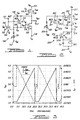
- FIG. 1 An example of a known read-out circuit for a photovoltaic detector is set forth in FIG. 1. This type of circuit is contemplated by the invention disclosed in co-pending U.S. Patent Application Nos. US-A-4786831 and US-A-4978872, assigned to the same assignee as this invention.
- Autozero capacitance 140 of transimpedance amplifier 100 of FIG. 1 is designed used for applications in which a stable detector bias is desired.
- Photovoltaic infrared detecting diode 101 has its anode terminal connected to bias source 112 which provides a voltage V ooM to the anode terminals of all other photovoltaic diodes in the focal plane array.
- a cathode electrode of diode 101 is coupled to a first terminal of autozero capacitor C Az 140, one terminal of feedback capacitor C FB 130 and to a drain electrode of an electronic switch comprised of a MOSFET 102.
- a terminal 120 of MOSFET 102 is coupled to a substrate bias V ss , while the source electrode of MOSFET 102 is coupled to the predetermined bias value, for the photovoltaic detector at terminal 110 and designated V DET .
- a gate electrode of MOSFET 102 is coupled at terminal 111 for receipt of a reset signal RST which is additionally coupled to a second electronic switch comprising MOSFET 103 at a gate thereof.
- a second terminal of autozero capacitor 140 is coupled to a source electrode of MOSFET 103 while a second terminal of the feedback capacitor 130 is coupled to the drain electrode of MOSFET 103.
- a substrate bias potential V ss is coupled to terminal 113 of MOSFET 103.
- An integrating amplifier which uses C FB 130 comprises MOSFET 105 having a gate electrode coupled to the source electrode of MOSFET 103, a bias potential V CAS coupled to a cascode gate of MOSFET 105 at terminal 119, a source electrode 118 coupled to bias source V ss and a drain electrode coupled to the read-out amplifier's output at terminal 117, the output voltage being designated V OUT . Also coupled to the output at 117 is the drain electrode of MOSFET 103 and a drain electrode of an active load MOSFET 104.
- a gate electrode of MOSFET 104 at terminal 114 is coupled to a bias voltage source V LD , while the source electrode of MOSFET 104 is coupled at terminal 115 to a bias Source V DD .
- a substrate bias source V suB is coupled to device 104 at terminal 116.
- an anode electrode of photovoltaic infrared detecting diode 201 is coupled to a return source of bias V coM at terminal 210.
- a cathode electrode of diode 201 is coupled to a source electrode of MOSFET switch 202, to a first terminal of feedback capacitor C FB 230, and a gate electrode of integrator driver amplifier MOSFET 203.
- the gate electrode 211 of the first MOSFET switch 202 is coupled for receipt of the first resetting enable signal RST1, while the drain electrode of switch 202 is coupled at terminal 212 to the desired bias voltage to be applied during the reset interval to diode 201 designated V DET .
- a substrate bias voltage V SUB is coupled to switch 202 at terminal 213.
- the source electrode of integrator driver 203 is coupled at terminal 217 to bias potential V DD while the drain electrode of driver 203 is coupled to a second terminal of feedback capacitor 230, an output terminal of the read-out amplifier 219 (carrying the output voltage designated V OUT ) and the respective drain electrodes of a second reset switch MOSFET 204 and MOSFET 205 which serves as the principle element of a self-calibrating active load for the read-out amplifier shown.
- a suitable substrate bias source V SUB is coupled to terminal 218 of MOSFET 203.
- Driver transistor 203 is of the PMOS type which has lower noise generating characteristics than NMOS type devices.
- a gate electrode of second reset switch 204 is coupled at terminal 214 for receipt of a second reset signal RST2.
- An appropriate substrate bias voltage V ss is coupled to switch 204 at terminal 220, while the source electrode of switch 204 is coupled to a first terminal of autozero capacitor C Az 240 and to a gate electrode of dynamic load MOSFET 205.
- a second terminal of autozero capacitor 240 and the source electrode of MOSFET 205 are coupled to bias potential supply V ss at terminal 215.
- MOSFETs 202 and 204 function simply as on/off electronic switches. These switches are both closed during the reset period of the amplifier and open during the read-out or integration period.
- V DET the desired detector bias voltage
- the desired detector bias voltage, V DET appears at the gate of the integrator driver MOSFET 203. This voltage defines the current, I DD , through integrator driver MOSFET 203 and active load MOSFET 205.
- the voltage on the gate of MOSFET 205 becomes the value required to allow 1 00 to flow through the drain-to-source circuit of load MOSFET 205.
- Both switches 202 and 204 are open, or in a high impedance state, during the integration.
- Autozero capacitor 240 maintains the reset voltage of the gate of MOSFET 205 at a level such as to cause MOSFET 205 to continue sinking current 1 00 established during the reset period.
- High gain around the feedback loop causes the gate of driver 203 to be held at a voltage such that driver 203 conducts the same amount of current as the active load device 205. Since the current through the active load 205 is the same as that defined by driver 203 during reset, the desired detector bias voltage is held on the gate of MOSFET 203 and the detector diode 201 by the feedback amplifier (driver 203 and feedback capacitor 230).
- a cascode gate 216 or, alternatively, a separate cascode transistor (not shown) can be added to driver MOSFET 203 as shown in Fig. 2 at terminal 216.
- the cascode gate tends to greatly increase the open loop gain of the integrator driver, because the cascode gate forces a constant voltage across the drain-to-source of the driver MOSFET 203 (analogous to the operation of a transistor source follower), resulting in the zeroing out of the drain-to-source conductance of device 203. Since it can be mathematically shown that the open loop gain is inversely proportional to the drain-to-source conductance of device 203, forcing this term to zero will result in the desired open loop gain increase.
- a typical sequence of operation of the circuit of Fig. 2 begins with the closure of the first and second electronic switches 202 and 204 (by a logical low signal appearing at input RST1 and a logical high signal appearing at the gate input of 204 at RST2).
- the closure or low impedance state of the source-to-drain of switch 202 places the detector bias voltage V DET onto the gate of driver MOSFET 203 resulting in a source to drain current I DD .
- the closure of switch 204 from source-to-drain couples the drain and gate of active load 205 to generate sufficient conduction through load 205 to sink current 1 00 to bias supply V ss at terminal 215.
- the signal RST2 at terminal 214 goes to the logical zero or low state to turn switch 204 off.
- the autozero capacitor 240 holds a voltage sufficient to continue sinking I DD through load 205 (a so-called auto-biasing scheme).
- RST1 goes high or to logic one to turn off switch 202, thereby initiating the integration period wherein the voltage on the photovoltaic detector 201 will be determined by the capacitive feedback loop of the integrator amplifier.
- V OUT will go more positive as the current through the photovoltaic detector 201 is integrated.
- the more light elements or photons impinging upon the detector during the integration interval the higher the slope of the output voltage of the read-out amplifier.
- the circuit of Fig. 2 has been simulated in the time domain through use of a computerized circuit analysis program.
- the pertinent wave forms predicted by the computerized simulation are set forth in Fig. 3 and demonstrate a debiasing or change in the bias voltage applied to the photovoltaic detecting diode of on the order of only 1.5 millivolts.
Landscapes
- Engineering & Computer Science (AREA)
- Power Engineering (AREA)
- Amplifiers (AREA)
Claims (7)
dadurch gekennzeichnet, daß
Applications Claiming Priority (2)
| Application Number | Priority Date | Filing Date | Title |
|---|---|---|---|
| US07/098,155 US4794247A (en) | 1987-09-18 | 1987-09-18 | Read-out amplifier for photovoltaic detector |
| US98155 | 2002-03-14 |
Publications (2)
| Publication Number | Publication Date |
|---|---|
| EP0331695A1 EP0331695A1 (de) | 1989-09-13 |
| EP0331695B1 true EP0331695B1 (de) | 1992-11-04 |
Family
ID=22267566
Family Applications (1)
| Application Number | Title | Priority Date | Filing Date |
|---|---|---|---|
| EP88907520A Expired EP0331695B1 (de) | 1987-09-18 | 1988-08-15 | Verstärker zur ablesung eines fotodetektors |
Country Status (6)
| Country | Link |
|---|---|
| US (1) | US4794247A (de) |
| EP (1) | EP0331695B1 (de) |
| JP (1) | JPH02501254A (de) |
| DE (1) | DE3875722T2 (de) |
| IL (1) | IL87466A (de) |
| WO (1) | WO1989002674A1 (de) |
Families Citing this family (19)
| Publication number | Priority date | Publication date | Assignee | Title |
|---|---|---|---|---|
| DE4041761A1 (de) * | 1990-12-24 | 1992-06-25 | Standard Elektrik Lorenz Ag | Stromsenke |
| US6493030B1 (en) | 1998-04-08 | 2002-12-10 | Pictos Technologies, Inc. | Low-noise active pixel sensor for imaging arrays with global reset |
| US6697111B1 (en) | 1998-04-08 | 2004-02-24 | Ess Technology, Inc. | Compact low-noise active pixel sensor with progressive row reset |
| US6535247B1 (en) | 1998-05-19 | 2003-03-18 | Pictos Technologies, Inc. | Active pixel sensor with capacitorless correlated double sampling |
| US6532040B1 (en) | 1998-09-09 | 2003-03-11 | Pictos Technologies, Inc. | Low-noise active-pixel sensor for imaging arrays with high speed row reset |
| US6587142B1 (en) | 1998-09-09 | 2003-07-01 | Pictos Technologies, Inc. | Low-noise active-pixel sensor for imaging arrays with high speed row reset |
| US6323479B1 (en) | 1998-09-16 | 2001-11-27 | Dalsa, Inc. | Sensor pixel with linear and logarithmic response |
| US6587146B1 (en) * | 1998-11-20 | 2003-07-01 | Eastman Kodak Company | Three transistor active pixel sensor architecture with correlated double sampling |
| US6809767B1 (en) * | 1999-03-16 | 2004-10-26 | Kozlowski Lester J | Low-noise CMOS active pixel sensor for imaging arrays with high speed global or row reset |
| US6750912B1 (en) | 1999-09-30 | 2004-06-15 | Ess Technology, Inc. | Active-passive imager pixel array with small groups of pixels having short common bus lines |
| US6498331B1 (en) | 1999-12-21 | 2002-12-24 | Pictos Technologies, Inc. | Method and apparatus for achieving uniform low dark current with CMOS photodiodes |
| US6873359B1 (en) | 2000-09-29 | 2005-03-29 | Rockwell Science Center, Llc. | Self-adjusting, adaptive, minimal noise input amplifier circuit |
| US6504141B1 (en) | 2000-09-29 | 2003-01-07 | Rockwell Science Center, Llc | Adaptive amplifier circuit with enhanced dynamic range |
| US6900839B1 (en) * | 2000-09-29 | 2005-05-31 | Rockwell Science Center, Llc | High gain detector amplifier with enhanced dynamic range for single photon read-out of photodetectors |
| US6965707B1 (en) | 2000-09-29 | 2005-11-15 | Rockwell Science Center, Llc | Compact active pixel with low-noise snapshot image formation |
| US6538245B1 (en) | 2000-10-26 | 2003-03-25 | Rockwell Science Center, Llc. | Amplified CMOS transducer for single photon read-out of photodetectors |
| US6888572B1 (en) | 2000-10-26 | 2005-05-03 | Rockwell Science Center, Llc | Compact active pixel with low-noise image formation |
| US6933771B2 (en) * | 2003-07-15 | 2005-08-23 | Stanley D. Stearns | Optically generated isolated feedback stabilized bias |
| US7363186B1 (en) * | 2006-12-22 | 2008-04-22 | Kelsey-Haynes Company | Apparatus and method for self calibration of current feedback |
Family Cites Families (7)
| Publication number | Priority date | Publication date | Assignee | Title |
|---|---|---|---|---|
| US3636458A (en) * | 1968-10-16 | 1972-01-18 | Yokogawa Electric Works Ltd | Periodic averaging circuit |
| JPS5413087Y2 (de) * | 1972-09-21 | 1979-06-05 | ||
| US4313067A (en) * | 1979-07-16 | 1982-01-26 | Miles Laboratories, Inc. | Sensor-integrator system |
| US4439693A (en) * | 1981-10-30 | 1984-03-27 | Hughes Aircraft Co. | Sample and hold circuit with improved offset compensation |
| US4567363A (en) * | 1983-06-20 | 1986-01-28 | Santa Barbara Research Center | Switched capacitor transresistance amplifier |
| US4578646A (en) * | 1984-02-08 | 1986-03-25 | Hitachi, Ltd | Integral-type small signal input circuit |
| US4684800A (en) * | 1986-03-14 | 1987-08-04 | Hughes Aircraft Company | Low-noise charge-injection method and apparatus for IR CCD scanning |
-
1987
- 1987-09-18 US US07/098,155 patent/US4794247A/en not_active Expired - Lifetime
-
1988
- 1988-08-15 WO PCT/US1988/002754 patent/WO1989002674A1/en not_active Ceased
- 1988-08-15 DE DE8888907520T patent/DE3875722T2/de not_active Expired - Fee Related
- 1988-08-15 EP EP88907520A patent/EP0331695B1/de not_active Expired
- 1988-08-15 JP JP63506503A patent/JPH02501254A/ja active Pending
- 1988-08-16 IL IL87466A patent/IL87466A/xx not_active IP Right Cessation
Also Published As
| Publication number | Publication date |
|---|---|
| WO1989002674A1 (en) | 1989-03-23 |
| US4794247A (en) | 1988-12-27 |
| JPH02501254A (ja) | 1990-04-26 |
| IL87466A (en) | 1992-01-15 |
| EP0331695A1 (de) | 1989-09-13 |
| DE3875722T2 (de) | 1993-04-15 |
| DE3875722D1 (de) | 1992-12-10 |
Similar Documents
| Publication | Publication Date | Title |
|---|---|---|
| EP0331695B1 (de) | Verstärker zur ablesung eines fotodetektors | |
| US5812030A (en) | Amplifier device capable of carrying out a stable amplifying operation without a gain variation | |
| KR930007482B1 (ko) | 전류검출회로 | |
| US8013660B2 (en) | System and method for charge integration | |
| US6252462B1 (en) | Capacitor transimpedance amplifier ( CTIA) with shared load | |
| US8416326B2 (en) | Method and apparatus for processing a pixel signal | |
| US6121843A (en) | Charge mode capacitor transimpedance amplifier | |
| US5650622A (en) | Infrared image pickup device | |
| US6140878A (en) | Transimpedance-type amplifier circuit with interchangeable resistance | |
| US5399989A (en) | Voltage amplifying source follower circuit | |
| US6501064B2 (en) | Image sensor with active sensor elements | |
| US6967682B1 (en) | Photoelectric converting device | |
| US6111245A (en) | Low voltage reverse bias arrangement for an active pixel sensor | |
| US4567363A (en) | Switched capacitor transresistance amplifier | |
| US5892220A (en) | Linearized feedback element for two-beam smart pixel receivers | |
| KR100436074B1 (ko) | 안정한 저전압동작이 가능한 증폭형 고체촬상장치용출력회로 | |
| US5021747A (en) | Symmetrical variable impedance apparatus employing MOS transistors | |
| US4728828A (en) | Switched capacitor transresistance amplifier | |
| US4929913A (en) | GaAs focal plane array readout | |
| Meyer et al. | Monolithic AGC loop for a 160 Mb/s transimpedance amplifier | |
| US5012134A (en) | DC bootstrapped unity gain buffer | |
| EP0261657A2 (de) | Eingangskreis für ein Infrarot-Abbildungsverfahren | |
| EP0642219B1 (de) | Verstärker | |
| US6528775B2 (en) | Charge-reading circuit protected against overloads coming from charges with undesirable polarity | |
| US5065114A (en) | Circuit configuration for an amplifier stage |
Legal Events
| Date | Code | Title | Description |
|---|---|---|---|
| PUAI | Public reference made under article 153(3) epc to a published international application that has entered the european phase |
Free format text: ORIGINAL CODE: 0009012 |
|
| 17P | Request for examination filed |
Effective date: 19890505 |
|
| AK | Designated contracting states |
Kind code of ref document: A1 Designated state(s): DE FR GB IT NL |
|
| 17Q | First examination report despatched |
Effective date: 19910808 |
|
| GRAA | (expected) grant |
Free format text: ORIGINAL CODE: 0009210 |
|
| AK | Designated contracting states |
Kind code of ref document: B1 Designated state(s): DE FR GB IT NL |
|
| REF | Corresponds to: |
Ref document number: 3875722 Country of ref document: DE Date of ref document: 19921210 |
|
| ITF | It: translation for a ep patent filed | ||
| ET | Fr: translation filed | ||
| PLBE | No opposition filed within time limit |
Free format text: ORIGINAL CODE: 0009261 |
|
| STAA | Information on the status of an ep patent application or granted ep patent |
Free format text: STATUS: NO OPPOSITION FILED WITHIN TIME LIMIT |
|
| 26N | No opposition filed | ||
| PGFP | Annual fee paid to national office [announced via postgrant information from national office to epo] |
Ref country code: FR Payment date: 19940711 Year of fee payment: 7 |
|
| PGFP | Annual fee paid to national office [announced via postgrant information from national office to epo] |
Ref country code: GB Payment date: 19940715 Year of fee payment: 7 |
|
| PGFP | Annual fee paid to national office [announced via postgrant information from national office to epo] |
Ref country code: DE Payment date: 19940720 Year of fee payment: 7 |
|
| PGFP | Annual fee paid to national office [announced via postgrant information from national office to epo] |
Ref country code: NL Payment date: 19940831 Year of fee payment: 7 |
|
| PG25 | Lapsed in a contracting state [announced via postgrant information from national office to epo] |
Ref country code: GB Effective date: 19950815 |
|
| PG25 | Lapsed in a contracting state [announced via postgrant information from national office to epo] |
Ref country code: NL Effective date: 19960301 |
|
| GBPC | Gb: european patent ceased through non-payment of renewal fee |
Effective date: 19950815 |
|
| PG25 | Lapsed in a contracting state [announced via postgrant information from national office to epo] |
Ref country code: FR Effective date: 19960430 |
|
| NLV4 | Nl: lapsed or anulled due to non-payment of the annual fee |
Effective date: 19960301 |
|
| PG25 | Lapsed in a contracting state [announced via postgrant information from national office to epo] |
Ref country code: DE Effective date: 19960501 |
|
| REG | Reference to a national code |
Ref country code: FR Ref legal event code: ST |
|
| PG25 | Lapsed in a contracting state [announced via postgrant information from national office to epo] |
Ref country code: IT Free format text: LAPSE BECAUSE OF NON-PAYMENT OF DUE FEES;WARNING: LAPSES OF ITALIAN PATENTS WITH EFFECTIVE DATE BEFORE 2007 MAY HAVE OCCURRED AT ANY TIME BEFORE 2007. THE CORRECT EFFECTIVE DATE MAY BE DIFFERENT FROM THE ONE RECORDED. Effective date: 20050815 |