EP0325427B1 - Dispositif d'amélioration d'une forme d'onde - Google Patents
Dispositif d'amélioration d'une forme d'onde Download PDFInfo
- Publication number
- EP0325427B1 EP0325427B1 EP89300444A EP89300444A EP0325427B1 EP 0325427 B1 EP0325427 B1 EP 0325427B1 EP 89300444 A EP89300444 A EP 89300444A EP 89300444 A EP89300444 A EP 89300444A EP 0325427 B1 EP0325427 B1 EP 0325427B1
- Authority
- EP
- European Patent Office
- Prior art keywords
- signal
- waveform
- differentiation
- full
- output
- Prior art date
- Legal status (The legal status is an assumption and is not a legal conclusion. Google has not performed a legal analysis and makes no representation as to the accuracy of the status listed.)
- Expired - Lifetime
Links
- 230000004069 differentiation Effects 0.000 claims description 55
- 230000008859 change Effects 0.000 claims description 23
- 238000005070 sampling Methods 0.000 claims description 10
- 230000000630 rising effect Effects 0.000 claims description 8
- 238000007493 shaping process Methods 0.000 claims description 8
- 238000001514 detection method Methods 0.000 claims 3
- 238000010586 diagram Methods 0.000 description 13
- 230000002596 correlated effect Effects 0.000 description 3
- 230000000875 corresponding effect Effects 0.000 description 3
- 230000000694 effects Effects 0.000 description 3
- 230000006872 improvement Effects 0.000 description 3
- 238000000034 method Methods 0.000 description 3
- 230000004044 response Effects 0.000 description 3
- 230000003111 delayed effect Effects 0.000 description 2
- 230000007257 malfunction Effects 0.000 description 2
- 230000008569 process Effects 0.000 description 2
- 230000008901 benefit Effects 0.000 description 1
- 239000003086 colorant Substances 0.000 description 1
Images


Classifications
-
- H—ELECTRICITY
- H04—ELECTRIC COMMUNICATION TECHNIQUE
- H04N—PICTORIAL COMMUNICATION, e.g. TELEVISION
- H04N5/00—Details of television systems
- H04N5/14—Picture signal circuitry for video frequency region
- H04N5/142—Edging; Contouring
Definitions
- This invention relates to a waveform improving circuit for improving the waveform contour of a signal whose band is reduced such as, for example, a chrominance signal reproduced in a video tape recorder (VTR).
- VTR video tape recorder
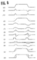
- Fig. 12 is a block diagram showing a conventional circuit for this purpose.
- Figs. 13(A) through (H) are diagrams showing the waveforms of signals of the circuit in Fig. 12. Referring to Fig. 12 and Figs. 13(A) through (H), a color difference signal a whose band is reduced is inputted to a terminal 30 and differentiated by a differentiation circuit 31 to be a signal b.
- the signal b thus obtained is subjected to a full-wave rectification by a full-wave rectification circuit 32 to be a signal c.
- the signal c thus obtained is waveform-shaped by a waveform shaping circuit 33 to be a signal d.
- the input signal a is subjected to sample-hold in response to this signal d by a sample-hold circuit 34 thereby to obtain an output signal e.
- the output signal e is improved in the contour of its waveform but a deviation of time t is taken place at the edge portion thereof.
- US-A-4331971 discloses a controller for use in conjunction with a bandwidth enhancement scheme in a colour television receiver.
- derivatives of the luminance and chrominance signals of an incoming video signal are used as control signals for the enhancement scheme, which acts to enhance the bandwidth of the chrominance element.
- the present invention provides a waveform improving apparatus arranged to improve a contour of a waveform of a first signal which has a slope portion at each of rising and falling edges thereof, comprising control pulse generating means arranged to generate, by differentiation, two control pulses and sampling and holding means responsive to said control pulses to output a waveform improved signal as the output of said apparatus; characterised by further comprising: waveform adjusting means arranged to raise a level at substantially the center of a rising slope portion of the waveform of said first signal, which is a component of a television signal, to be substantially equal to a level at the uppermost end of the rising slope portion and to reduce a level at substantially the center of a falling slope portion of the waveform of said first signal to be substantially equal to a level at the lowermost end of the falling slop portion, thereby to obtain a waveform-adjusted signal; wherein the control pulse generating means comprises means arranged to differentiate twice a second signal, which is another component of the said television signal, and has a correlation to the first signal
- the present invention therefore provides a waveform improving apparatus which improves the waveform contour of a signal whose frequency band is reduced.
- the present invention is advantageously applicable to a video signal, which contains a luminance signal and a chrominance signal including a chrominance-difference signal, or which contains three primary color signals.
- the first signal may be a chrominance signal, and at this time the second signal may be either a luminance signal or the chrominance signal.
- Both the first and second signal may be a luminance signal.
- the first signal may be one of the three primary color signals, and at this time the second signal may be either the same as the first signal or another of the three primary color signals.
- the first and second signals may be selected such that they are correlated to each other.
- it is preferable to use a luminance signal as the second signal because the luminance signal generally has a high signal to noise ratio and a high frequency band. Both a luminance signal and a chrominance signal may be used for producing the control pulses.
- a waveform adjusting circuit for performing the waveform adjusting of the input first signal comprises: a differentiation circuit for differentiating the first signal; and an adder for adding the input first signal and an output of the differentiation circuit.
- a control pulse generating circuit for producing the control pulses from the second signal comprises: a first differentiation circuit for differentiating the input second signal; a full-wave rectification circuit for full-wave-rectifying an output of the first differentiation circuit; and a second differentiation circuit for differentiating an output of the full-wave rectification circuit.
- a waveform-adjusted first signal outputted from the waveform adjusting circuit is fed to a sample-and-hold circuit which is responsive to each control pulse outputted from the control pulse generating circuit for sampling and holding the waveform-adjusted first signal to obtain a waveform contour improved first signal.
- the waveform adjusting circuit may include a delay circuit for compensating a delay caused in the control pulse generating circuit.
- the control pulse generating circuit may include a waveform shaping circuit for shaping a pulse outputted from the second differentiation circuit into a rectangular waveform pulse.
- the control pulse generating circuit is provided before the first differentiation circuit with a low-pass filter for limiting the frequency band of the first signal so that each of the control pulses generated by the control pulse generating circuit has a proper pulse width.
- this low-pass filter may reduce the band of the second signal to be approximately the same as the band of the first signal.
- control pulse generating circuit may further comprise: a third differentiation circuit for differentiating the first signal; an additional full-wave rectification circuit for full-wave-rectifying an output of the third differentiation circuit; and an adder for adding outputs of the full-wave rectification circuit and the additional full-wave rectification circuit, an output of the adder being fed to the second differentiation circuit.
- This structure is advantageous in a case that the second signal is not always correlated to the first signal.
- This structure may be further modified such that a multiplier is provided between the first differentiation circuit and the full-wave rectification circuit for multiplying the outputs of the first and third differentiation circuits or between the full-wave rectification circuit and the adder for multiplying the outputs of the two full-wave rectification circuits.
- the multiplier operates as a kind of gate for passing the output of the first differentiation circuit to the second differentiation circuit only when there is a change in the first signal.
- control pulse generating circuit may have a gate circuit which is inserted to any position after the first differentiation circuit for passing the output information of the first differentiation circuit to the subsequent stage only when there is a change in the first signal.
- a circuit for detecting a change in the first signal is provided for producing a gate control signal for the gate circuit.
- the control pulse generating circuit may further comprises: an additional low-pass having a higher response than that of the low-pass filter provided before the first differentiation circuit for limitinng the band of the input second (luminance) signal; and additional differentiation circuit for differentiating an output of the additional low-pass filter; and an adder for adding outputs of the first and additional differentiation circuits, an output of the adder being fed to the full-wave rectification circuit.
- Fig. 1 is a block diagram showing a waveform improving apparatus in accordance with a first embodiment of this invention
- Fig. 2 shows waveforms of signals of the components of the circuit in Fig. 1.
- the reference letters (a) through (k) are designated correspondingly to each other. Since a video signal has a luminance signal and a color difference signal which are strongly correlated to each other, it may be considered that the luminance signal changes when the color difference signal changes. Therefore, in this first embodiment, a control signal f is obtained from the luminance signal.
- a luminance signal a inputted into a terminal 1 is sent to control signal generating circuit 3.
- the frequency band of the input signal is limited by a low-pass filter (LPF) 6 to be a signal b.
- the band-limited signal b is differentiated by a first differentiation circuit 7 to be a signal c.
- the signal c thus obtained is subjected to a full-wave rectification by a full-wave rectification circuit 8 to be a signal d.
- the signal d thus obtained is differentiated by a second differentiation circuit 9 to be a signal e.
- a waveform shaping circuit 10 detects a positive pulse portion of the signal c thus differentiated to obtain a control signal f.
- the control signal f thus obtained occurs from the beginning point of each edge slope part of the signal b to the center of the same.
- a color difference signal g (for example, R-Y or B-Y signal) is inputted to a terminal 2 and then fed to a waveform adjusting circuit 4.
- the color difference signal g is inputted to a delay circuit 11 which has a suitable delay time corresponding to a processing time in the control signal generating circuit 3, and, at the same time, inputted to a differentiation circuit 12.
- An output signal h of the differentiation circuit 12 is sliced at a small level by a slice circuit 13 in order to eliminate noise components thereby to obtain a signal i.
- the slice circuit 13 is not an inherently necessary circuit, and may be omitted.
- the signal i is added by an adder 14 with the output of the delay circuit 11 to obtain a signal j.
- the signal j thus obtained is subjected to sample-hold in response to the control signal f by a sample-hold circuit 5 to obtain a waveform contour improved signal k, which is outputted from a terminal 15.
- the waveform contour improving effect can be clearly seen by comparing the signal k with the input band-reduced signal g.
- the output signal i of the slice circuit 13 is not added with the output of the delay circuit 11, the output signal k becomes as shown in l, so that the contour improving effect is halved. Therefore, it is preferable that the signal i is added with the output of the delay circuit 11 by the adder 14 so as to obtain the waveform of the signal k.
- the delay circuit 11 may be or may not be included in the waveform adjusting circuit 4.
- Fig. 2 (m) is a diagram schematically superposing the input signal g, the signal j and the output signal k. This clearly shows that the waveform contour is largely improved and yet no time delay at the edge portion of the output signal is generated.
- a waveform improving circuit of this invention achieves the waveform contour improving process of a signal at the center of each edge slope of the waveform thereof, which means that there is no time lag due to process.
- the luminance signal is indicated as signal a.
- waveforms a through f as schematically illustrated in Figs. 3(A)-(E) are produced an consequently the signal to be outputted will become as shown at k.
- reference letters a through k in Fig. 3 correspond to the reference letters a through k in Fig. 1, respectively.
- the control signal f lasts almost through the interval of red, so that if sample-hold is made before the color difference signal indicates red an interval where the image is not colored is possibly generated. This is not preferable.
- a second embodiment of the control signal generating circuit 4 of the waveform improving circuit of this invention is shown in Fig. 4.
- a low-pass filter (LPF) 16 As clearly shown in Fig. 4 are disposed a low-pass filter (LPF) 16, a differentiation circuit 17 and an adder 18 additionally to the circuit shown in Fig. 1.
- the LPF 16 has a cut-off frequency which is higher than that of the LPF 6 shown in Fig. 1.
- the waveforms of signals of the components of the circuit in Fig. 4 are shown in Figs. 5(A) through (H), respectively.
- the luminance signal a is band-limited by the LPF 16 to be a signal b1 which is subsequently differentiated by the differentiation circuit 17 to be a signal c1.
- the differential signal c1 is added by the adder 18 to the differential signal c and rectified thereby to produce the signal d.
- the secondary differential signal becomes as an signal e and the control signal f is obtained.
- Color difference output signals obtained when the color difference signal is subjected to the sample-hold by the signal f in Fig. 5 and the signal f in Fig. 3 are shown in Figs. 6(A) through (G), respectively.
- Fig. 6 In Fig. 6 are shown the luminance signal a, color difference signal g, added signal j, signal f1 which is identical to the signal f shown in Fig. 3, signal k1 which is produced by use of signal f1, signal f2 which is identical to the signal f shown in Fig. 5, and signal k2 which is produced by use of signal f2.
- signal k2 In the signal k2, such a decoloration as is seen in the case of the signal k1 is not generated.
- Fig. 7 is a block diagram showing a waveform improving apparatus in accordance with a third embodiment of the invention
- Fig. 8 shows waveforms of signals from the components of the apparatus in Fig. 7.
- Reference letters shown in Fig. 7 and Figs. 8(a) to (k) are designated correspondingly to each other.
- the control signal for improving the edge of a chrominance signal is made from the information on the change in chrominance signal is made from the information on the change in chrominance signal and the information on the change in luminance signal.
- a luminance signal a inputted to a terminal 1 is differentiated by a differentiation circuit 7 to obtain a signal b.
- a color difference signal d which is input to a terminal 2 is differentiated by a differentiation circuit 20 to obtain a signal e.
- the two signals b and c are subjected to full-wave rectification by full-wave rectification circuits 8 and 21 to obtain signals c and f, respectively.
- the signals c and f thus obtained are added by an adder 22 to output a signal g.
- the signal g is differentiated by a differentiation circuit 9 to output a signal h.
- the signal h is waveform-shaped by a waveform shaping circuit 10 thereby to obtain a control signal i.
- the luminance signal a is generally superior in S/N ratio to the color difference signal d, so that it is preferable that the control signal is obtained from the luminance signal.
- a video signal has no change in luminance signal but changes only in color difference signal
- it is impossible to generate the control signal which means that the waveform contour improvement is impossible to be achieved.
- the information on the luminance signal is used, and, on the other hand, when there exists no change in the luminance signal, the control signal is generated from the change in the color difference signal.
- This function is accomplished by the arrangement as shown in Fig. 7.
- a fourth embodiment of the control signal generating circuit is shown in Fig. 9.
- the differential signal b of the luminance signal a is fed to a gate circuit 23.
- the gate circuit 23 is controlled by the signal f which is obtained through the full-wave recification of the differential signal e of the color difference signal d.
- the gate circuit 23 is turned ON when the signal f becomes a specific output level.
- a control signal i is obtained using the information on the change in the luminance signal only when the color difference signal is being changed. This means that when the color difference signal has no change, no control signal is generated, so that such a malfunction that may execute a sample-hold at an unnecessary timing will be prevented from taking place.
- the gate circuit 23 can be insertedly disposed at any position in the path from the front of the full-wave rectification circuit 8 to the rear of the waveform shaping circuit 10 in Fig. 9.
- a fifth embodiment of the control signal generating circuit is shown in Fig. 10 in a block diagram form.
- a multiplier 24 is used instead of the gate circuit 23 in Fig. 9 and an adder 22 is insertedly used successively thereto.
- the waveform contour of the color difference signal can be improved based on the change in the luminance signal which is superior in S/N ratio, and when there exists no correlation between the change in the luminance signal and the change in the color difference signal, the waveform contour is improved by the information on the change of the color difference signal itself.
- the delay circuit 11 in order to construct the waveform adjusting circuit 4, can be disposed at either front portion of the differentiation circuit 12 or rear portion of the adder 14 as shown in Figs. 11(A) and (B).
- the delay circuit in the waveform adjusting circuit 4 is not always necessary and may be omitted.
- the luminance signal and color difference signal are exemplified as the two input signals of the apparatus of this invention, but the two input signals may be identical to each other.
- both of the two input signals are a color difference signal or a luminance signal.
- the LPF 6 in the control signal generating circuit 3 shown in the first embodiment of this invention may be omitted.
Claims (15)
- Dispositif d'amélioration d'une forme d'onde conçu pour améliorer le contour d'une forme d'onde d'un premier signal qui possède une partie inclinée en chacun de ses flancs adjacent et descendant, comportant des moyens de génération d'impulsions de commande conçus pour générer par différentiation, deux impulsions de commande et des moyens d'échantillonnage-blocage (5) sensibles auxdites impulsions de commande pour délivrer un signal de forme d'onde améliorée à la sortie dudit dispositif ;
caractérisé en ce qu'il comporte en outre :
des moyens de réglage de forme d'onde (4) conçus pour élever un niveau sensiblement au centre d'une partie inclinée ascendante de la forme d'onde dudit premier signal, qui constitue une composante d'un signal de télévision, pour le rendre sensiblement égal à un niveau à l'extrémité supérieure de la partie inclinée ascendante et pour réduire un niveau sensiblement au centre d'une partie inclinée descendante de la forme d'onde dudit premier signal pour le rendre sensiblement égal à un niveau à l'extrémité la plus basse de la partie inclinée descendante, pour ainsi obtenir un signal à forme d'onde réglée;
dans lequel les moyens de génération d'impulsions de commande (3) comportent des moyens agencés pour différentier deux fois un second signal, qui constitue une autre composante dudit signal de télévision, et possède une corrélation par rapport au premier signal, pour obtenir deux impulsions de commande possédant chacune une largeur d'impulsions prédéterminée, l'une des deux impulsions de commande se terminant à un instant correspondant sensiblement au centre de la partie ascendante de la forme d'onde du premier signal, et l'autre des deux impulsions de commande se terminant à un instant correspondant sensiblement au centre de la partie descendante de la forme d'onde du premier signal ; et
dans lequel les moyens d'échantillonnage-blocage (5) sont sensibles aux deux impulsions de commande pour échantillonner un niveau du signal à forme d'onde réglée sur un bord antérieur de chacune des deux impulsions de commande et bloquer un niveau échantillonné durant seulement une durée égale à la largeur d'impulsion prédéterminée pour ainsi obtenir un premier signal à forme d'onde améliorée. - Dispositif d'amélioration d'une forme d'onde selon la revendication 1, dans lequel lesdits moyens de réglage de forme d'onde (4) comportent :
des premiers moyens de différentiation (12) pour différentier le premier signal ; et
des moyens d'addition (14) pour additionner un signal de sortie des premiers moyens de différentiation et le premier signal pour obtenir le signal à forme d'onde réglée, et
lesdits moyens de génération d'impulsions de commande (3) comportent :
des seconds moyens de différentiation (7) pour différentier le second signal ;
des moyens de redressement à deux alternances (8) pour redresser les deux alternances d'un signal de sortie des seconds moyens de différentiation ; et
des troisièmes moyens de différentiation (9) pour différentier un signal de sortie des moyens de redressement à deux alternances pour obtenir les deux impulsions de commande. - Dispositif selon la revendication 2, comportant en outre des moyens de découpage (13) pour découper le signal de sortie des premiers moyens de différentiation (12) à un niveau prédéterminé pour éliminer des composantes de bruit.
- Dispositif selon la revendication 2, comportant en outre un filtre passe-bas (6) disposé en amont des seconds moyens de différentiation (7) pour limiter une bande de fréquence du second signal.
- Dispositif selon la revendication 2, dans lequel le premier signal est un signal de chrominance d'un signal vidéo et le second signal est un signal de luminance du signal vidéo.
- Dispositif selon la revendication 5, comportant en outre un filtre passe-bas (6) disposé en amont des seconds moyens de différentiation (7) pour limiter une bande de fréquence du signal de luminance.
- Dispositif selon la revendication 6, dans lequel le filtre passe-bas (6) limite la bande de fréquence du signal de luminance pour la rendre sensiblement égale à une bande de fréquence du signal de chrominance.
- Dispositif selon la revendication 6, comportant en outre :
un filtre passe-bas supplémentaire (16) possédant une fréquence de coupure supérieure à celle du filtre passe-bas (6) pour limiter la bande de fréquence du signal de luminance ;
des quatrièmes moyens de différentiation (17) pour différentier un signal de sortie du filtre passe-bas supplémentaire (16) ; et
des moyens d'addition supplémentaires (18) disposés entre les seconds moyens de différentiation (7) et les moyens de redressement à deux alternances (8) pour additionner le signal de sortie des seconds moyens de différentiation et un signal de sortie des quatrièmes moyens de différentiation (17), un signal de sortie des moyens d'addition supplémentaires étant appliqué aux moyens de redressement à deux alternances. - Dispositif selon la revendication 2, comportant en outre :
des moyens de détection (20, 21) pour détecter une variation du premier signal pour obtenir un signal de détection ; et
des moyens de déclenchement (23) disposés dans un trajet de signal allant des seconds moyens de différentiation (7) aux moyens d'échantillonnage-blocage (5) et sensibles au signal de détection pour transmettre une information au signal de sortie des seconds moyens de différentiation aux moyens d'échantillonnage-blocage uniquement lorsqu'une variation du premier signal se produit. - Dispositif selon la revendication 9, dans lequel les moyens de détection (20, 21) comportent :
des quatrièmes moyens de différentiation (20) pour différentier le premier signal ; et
des moyens de redressement à deux alternances (21) pour redresser les deux alternances d'un signal de sortie des quatrièmes moyens de différentiation pour obtenir le signal de détection. - Dispositif selon la revendication 2, comportant en outre :
des quatrièmes moyens de différentiation (20) pour différentier le premier signal ;
des moyens de redressement à deux alternances supplémentaires (21) pour redresser les deux alternances d'un signal de sortie des quatrièmes moyens de différentiation ; et
des moyens d'addition supplémentaires (22) disposés entre les moyens de redressement à deux alternances (8) et les troisièmes moyens de différentiation (9) pour additionner le signal de sortie des moyens de redressement à deux alternances et un signal de sortie des moyens de redressement à deux alternances supplémentaires (21) et appliquer le résultat de l'addition aux troisièmes moyens de différentiation. - Dispositif selon la revendication 11, dans lequel le premier signal est un signal de chrominance d'un signal vidéo et le second signal est un signal de luminance du signal vidéo.
- Dispositif selon la revendication 11, comportant en outre des moyens de déclenchement (24) disposés dans un trajet de signal allant des seconds moyens de différentiation (7) jusqu'aux moyens d'addition supplémentaires (22) et sensibles au signal de sortie des moyens de redressement à deux alternances supplémentaires (21) pour transmettre une information du signal de sortie des seconds moyens de différentiation aux moyens d'addition supplémentaires uniquement lorsque le signal de sortie des moyens de redressement à deux alternances supplémentaires dépasse un niveau prédéterminé.
- Dispositif selon la revendication 13, dans lequel les moyens de déclenchement (24) comportent des moyens de multiplication pour multiplier les signaux de sortie des moyens de redressement à deux alternances (8, 21) et appliquer le résultat de la multiplication aux moyens d'addition supplémentaires.
- Dispositif selon la revendication 2, comportant en outre des moyens de mis en forme (10) de la forme d'onde disposés entre les troisièmes moyens de différentiation (9) et les moyens d'échantillonnage-blocage (5) pour mettre en forme l'impulsion de commande en une impulsion de forme d'onde rectangulaire.
Applications Claiming Priority (4)
| Application Number | Priority Date | Filing Date | Title |
|---|---|---|---|
| JP63008729A JP2523747B2 (ja) | 1988-01-19 | 1988-01-19 | 輪郭改善回路 |
| JP63008728A JP2523746B2 (ja) | 1988-01-19 | 1988-01-19 | 輪郭改善回路 |
| JP8729/88 | 1988-01-19 | ||
| JP8728/88 | 1988-01-19 |
Publications (3)
| Publication Number | Publication Date |
|---|---|
| EP0325427A2 EP0325427A2 (fr) | 1989-07-26 |
| EP0325427A3 EP0325427A3 (fr) | 1991-07-03 |
| EP0325427B1 true EP0325427B1 (fr) | 1994-12-14 |
Family
ID=26343305
Family Applications (1)
| Application Number | Title | Priority Date | Filing Date |
|---|---|---|---|
| EP89300444A Expired - Lifetime EP0325427B1 (fr) | 1988-01-19 | 1989-01-18 | Dispositif d'amélioration d'une forme d'onde |
Country Status (3)
| Country | Link |
|---|---|
| US (1) | US4931858A (fr) |
| EP (1) | EP0325427B1 (fr) |
| DE (1) | DE68919863T2 (fr) |
Families Citing this family (9)
| Publication number | Priority date | Publication date | Assignee | Title |
|---|---|---|---|---|
| US5260774A (en) * | 1989-04-20 | 1993-11-09 | Canon Kabushiki Kaisha | White balance control for still image sensing apparatus |
| JPH0449781A (ja) * | 1990-06-19 | 1992-02-19 | Sony Corp | テレビジョン画像表示装置 |
| KR920008630B1 (ko) * | 1990-09-28 | 1992-10-02 | 삼성전자 주식회사 | 수평윤곽 보상회로 |
| WO1998011732A1 (fr) * | 1996-09-16 | 1998-03-19 | Philips Electronics N.V. | Amelioration du transitoire de la couleur percue |
| DE19639572A1 (de) * | 1996-09-26 | 1998-04-02 | Philips Patentverwaltung | Verfahren und Anordnung zur Farbkantenversteilerung |
| EP3194021B1 (fr) * | 2014-09-15 | 2018-10-24 | Boston Scientific Neuromodulation Corporation | Interface utilisateur graphique pour la programmation de schémas d'impulsions de neurostimulation |
| CN107073269B (zh) | 2014-11-04 | 2020-05-22 | 波士顿科学神经调制公司 | 用于编程复杂神经刺激模式的方法和装置 |
| EP3328481B1 (fr) | 2015-07-30 | 2019-05-15 | Boston Scientific Neuromodulation Corporation | Interface utilisateur de stimulation électrique à motifs personnalisés |
| US10456586B2 (en) | 2015-10-15 | 2019-10-29 | Boston Scientific Neuromodulation Corporation | User interface for neurostimulation waveform composition |
Family Cites Families (6)
| Publication number | Priority date | Publication date | Assignee | Title |
|---|---|---|---|---|
| DE2064731B2 (de) * | 1970-12-31 | 1973-06-07 | Robert Bosch Fernsehanlagen Gmbh, 6100 Darmstadt | Verfahren zur versteilerung von signalspruengen und schaltungsanordnung zur ausuebung des verfahrens |
| US4030121A (en) * | 1975-12-02 | 1977-06-14 | Faroudja Y C | Video crispener |
| US4181917A (en) * | 1977-07-01 | 1980-01-01 | Quadricolor Technology L.P. | Color television receiving system utilizing inferred high frequency signal components to reduce color infidelities in regions of color transitions |
| US4316215A (en) * | 1979-09-26 | 1982-02-16 | Matsushita Electric Industrial Co., Ltd. | System for improving reproduction of images in a color television receiver |
| US4331971A (en) * | 1980-11-19 | 1982-05-25 | Zenith Radio Corporation | Mode decision controller for selectively actuating a chrominance bandwith enhancement in a television receiver |
| DE3223580A1 (de) * | 1982-06-24 | 1983-12-29 | Philips Patentverwaltung Gmbh, 2000 Hamburg | Schaltungsanordnung zum erhoehen der schaerfe von farbkanten |
-
1989
- 1989-01-18 DE DE68919863T patent/DE68919863T2/de not_active Expired - Fee Related
- 1989-01-18 EP EP89300444A patent/EP0325427B1/fr not_active Expired - Lifetime
- 1989-01-19 US US07/298,980 patent/US4931858A/en not_active Expired - Lifetime
Also Published As
| Publication number | Publication date |
|---|---|
| DE68919863D1 (de) | 1995-01-26 |
| US4931858A (en) | 1990-06-05 |
| DE68919863T2 (de) | 1995-07-06 |
| EP0325427A3 (fr) | 1991-07-03 |
| EP0325427A2 (fr) | 1989-07-26 |
Similar Documents
| Publication | Publication Date | Title |
|---|---|---|
| US4072984A (en) | Chrominance-luminance separator | |
| US4084181A (en) | Apparatus for transmission of chrominance signals during blanking period | |
| EP0084241B1 (fr) | Dispositif de traitement de signal et méthode pour enregistrer sur une bande vidéo | |
| US4232330A (en) | Method and system for separating the chrominance and luminance signals in color television signals having quadrature-modulated chrominance subcarriers | |
| EP0617564A2 (fr) | Circuit pour l'ajustement automatique de séparation de signal dans un filtre à peigne pour séparation Y/C | |
| NL8201399A (nl) | Stelsel voor het opwekken van een chromasleutelschakelsignaal. | |
| EP0325427B1 (fr) | Dispositif d'amélioration d'une forme d'onde | |
| CA2047398C (fr) | Eliminateur de bruit dans les signaux de luminance | |
| US5047866A (en) | Comb filter type luminance/chrominance signal separation circuit | |
| EP0333480B1 (fr) | Dispositif de traitement de signal vidéo | |
| GB1480516A (en) | Aperture correction circuit | |
| CA1115412A (fr) | Suppression de la contamination des signaux de chrominance par des signaux de luminance dans un systeme de traitement de signaux video | |
| US4293869A (en) | Circuit for reducing drop-out errors in a video signal derived from a recording device | |
| EP0199602B1 (fr) | Circuit de traitement du signal | |
| US4689680A (en) | Circuit arrangement for generating clamping pulses | |
| EP0574200A1 (fr) | Dispositif numérique pour démodulation de signaux de chrominance | |
| US4101940A (en) | Circuit for delaying a composite video signal by a line duration, particularly for use with a video record player | |
| JP2523746B2 (ja) | 輪郭改善回路 | |
| US3808359A (en) | Playback circuit for a three line sequential color television signal | |
| EP0420184B1 (fr) | Circuit de traitement de signal vidéo | |
| EP0735779B1 (fr) | Démodulateur de signal couleur applicable pour télévision PAL et SECAM | |
| EP0668702B1 (fr) | Circuit de séparation des signaux de luminance et de chrominance | |
| US5159439A (en) | Circuit for controlling delay time between luminance and chrominance signals | |
| JP2638937B2 (ja) | Yc分離制御回路 | |
| JP2523747B2 (ja) | 輪郭改善回路 |
Legal Events
| Date | Code | Title | Description |
|---|---|---|---|
| PUAI | Public reference made under article 153(3) epc to a published international application that has entered the european phase |
Free format text: ORIGINAL CODE: 0009012 |
|
| AK | Designated contracting states |
Kind code of ref document: A2 Designated state(s): DE FR GB |
|
| PUAL | Search report despatched |
Free format text: ORIGINAL CODE: 0009013 |
|
| AK | Designated contracting states |
Kind code of ref document: A3 Designated state(s): DE FR GB |
|
| 17P | Request for examination filed |
Effective date: 19911218 |
|
| 17Q | First examination report despatched |
Effective date: 19931007 |
|
| GRAA | (expected) grant |
Free format text: ORIGINAL CODE: 0009210 |
|
| AK | Designated contracting states |
Kind code of ref document: B1 Designated state(s): DE FR GB |
|
| REF | Corresponds to: |
Ref document number: 68919863 Country of ref document: DE Date of ref document: 19950126 |
|
| ET | Fr: translation filed | ||
| PLBE | No opposition filed within time limit |
Free format text: ORIGINAL CODE: 0009261 |
|
| STAA | Information on the status of an ep patent application or granted ep patent |
Free format text: STATUS: NO OPPOSITION FILED WITHIN TIME LIMIT |
|
| 26N | No opposition filed | ||
| REG | Reference to a national code |
Ref country code: GB Ref legal event code: IF02 |
|
| PGFP | Annual fee paid to national office [announced via postgrant information from national office to epo] |
Ref country code: FR Payment date: 20020110 Year of fee payment: 14 |
|
| PGFP | Annual fee paid to national office [announced via postgrant information from national office to epo] |
Ref country code: GB Payment date: 20020116 Year of fee payment: 14 |
|
| PGFP | Annual fee paid to national office [announced via postgrant information from national office to epo] |
Ref country code: DE Payment date: 20020227 Year of fee payment: 14 |
|
| PG25 | Lapsed in a contracting state [announced via postgrant information from national office to epo] |
Ref country code: GB Free format text: LAPSE BECAUSE OF NON-PAYMENT OF DUE FEES Effective date: 20030118 |
|
| PG25 | Lapsed in a contracting state [announced via postgrant information from national office to epo] |
Ref country code: DE Free format text: LAPSE BECAUSE OF NON-PAYMENT OF DUE FEES Effective date: 20030801 |
|
| GBPC | Gb: european patent ceased through non-payment of renewal fee | ||
| PG25 | Lapsed in a contracting state [announced via postgrant information from national office to epo] |
Ref country code: FR Free format text: LAPSE BECAUSE OF NON-PAYMENT OF DUE FEES Effective date: 20030930 |
|
| REG | Reference to a national code |
Ref country code: FR Ref legal event code: ST |