EP0322077A2 - Optical backscattering device - Google Patents
Optical backscattering device Download PDFInfo
- Publication number
- EP0322077A2 EP0322077A2 EP88202965A EP88202965A EP0322077A2 EP 0322077 A2 EP0322077 A2 EP 0322077A2 EP 88202965 A EP88202965 A EP 88202965A EP 88202965 A EP88202965 A EP 88202965A EP 0322077 A2 EP0322077 A2 EP 0322077A2
- Authority
- EP
- European Patent Office
- Prior art keywords
- photodiode
- optical
- frequency
- voltage
- arrangement according
- Prior art date
- Legal status (The legal status is an assumption and is not a legal conclusion. Google has not performed a legal analysis and makes no representation as to the accuracy of the status listed.)
- Withdrawn
Links
Images
Classifications
-
- G—PHYSICS
- G01—MEASURING; TESTING
- G01M—TESTING STATIC OR DYNAMIC BALANCE OF MACHINES OR STRUCTURES; TESTING OF STRUCTURES OR APPARATUS, NOT OTHERWISE PROVIDED FOR
- G01M11/00—Testing of optical apparatus; Testing structures by optical methods not otherwise provided for
- G01M11/30—Testing of optical devices, constituted by fibre optics or optical waveguides
- G01M11/31—Testing of optical devices, constituted by fibre optics or optical waveguides with a light emitter and a light receiver being disposed at the same side of a fibre or waveguide end-face, e.g. reflectometers
- G01M11/3172—Reflectometers detecting the back-scattered light in the frequency-domain, e.g. OFDR, FMCW, heterodyne detection
Definitions
- the invention relates to an optical backscatter measuring device with an optical transmitter, the transmission power of which is modulated (wobbled) via an oscillator with a changing frequency and the transmission beam of which is conducted via a beam splitter into an optical waveguide (LWL), and with an optical receiver designed as a photodiode, to which portions of the transmitted beam which are scattered back from the optical fiber via the beam splitter are supplied and in which a mixed signal is formed from a signal proportional to the optical backscattering power and a modulation voltage having the oscillator frequency and is evaluated to determine the backscattering location and the backscattering intensity.
- LWL optical waveguide
- the invention has for its object to reduce the effort for the optical receiver.
- the photodiode is an avalanche photodiode, the bias voltage of which is a direct voltage modulated with the modulation voltage, and in that the mixed signal is tapped from an ohmic resistor R P and a capacitor C P in a parallel circuit connected to the excitation circuit of the photodiode .
- the ratio of the mixing frequency to the modulation frequency is less than 0.5 ⁇ 10 ⁇ 3. With larger ratios it is more difficult to separate the mixed signal from the modulation frequency voltage. It is preferably provided that the ohmic resistance R P is greater than 10 times, preferably greater than 20 times, the impedance related to the minimum value of the modulation frequency and less than 0.05 times, preferably 0.035 times, of the impedance of the capacitor C P related to the mixed frequency.
- a good signal yield also results from the fact that the apparent resistance of the series connection of the capacitor C P and the self-capacitance C D of the photodiode resulting from the greatest value of the modulation frequency is greater than 10 times, preferably 20 times the ohmic internal resistance R i of the excitation circuit for is the photodiode.
- the light backscattered from a specific backscattering location along the length of the optical fiber being examined can be detected in a targeted manner in that the mixed signal is transmitted via a Bandpass filter is passed and that shift frequencies are specified according to the distance to be considered from the backscatter.
- shorter measuring times result from the fact that the mixed signal is passed in parallel over several bandpass filters of different pass frequencies, so that several backscatter points spaced apart from one another can be measured simultaneously.
- the mixed signals are fed to a circuit for Fourier transformation. This allows you to reduce the measurement time to a minimum.
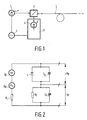
- the transmission beam from the laser diode 1 is directed via the beam splitter 2 into the optical fiber 3 to be measured. Parts of the transmitted beam which are scattered back from the LWL 3 are directed by the beam splitter 2 onto the receiver diode (APD) 4.
- the frequency-variable signal of the oscillator 5 wobbles on the one hand the light intensity of the laser diode 1 and on the other hand is used to form a mixed signal in the receiving and evaluating device 6.
- a series circuit consisting of an ohmic resistor R P and a capacitor C P is connected in series with the APD 4, which has an intrinsic capacitance C D.
- the sum voltage from the direct voltage U G and the modulation voltage U M proportional to the signal of the oscillator 5 is applied to the series circuit.
- the internal resistance of the two voltage sources is denoted by R i .
- the laser diode 1 is modulated and swept through the frequency f o to f max in a time T by means of the oscillator 5.
- the power of the transmission beam then changes according to the following equation: P (t) P ⁇ [1 + m L cos ( ⁇ c t + t2)]
- the bias of the APD is modulated at high frequency by a signal derived from the laser diode control.
- the APD is therefore used for reception and mixing at the same time.
- the components of the circuit according to FIG. 2 were dimensioned taking the following requirements into account: - In the range of the modulation frequencies [f o , f max ] the resistance should be R »1 / ⁇ C. - in the range [f o , f max ],
- This dimensioning ensures that the modulation voltage is applied to the APD with a low resistance, while the resistance R p occurs as a conversion resistance for the signals with the mixed frequency ⁇ f and can be chosen to be large.
- i ph (t) S ⁇ M (t)
- P s (t) S ⁇ RP ⁇ M o ⁇ 1 ⁇ 2m
- the spatial resolution is accordingly if v g is the speed of light in the optical fiber.
- the spatial resolution is therefore determined by the frequency range that runs through it.
- N 5000 measuring points must be recorded.
- a Teit T of approximately 1 s should be chosen.
- the measurement time can be reduced by a factor of 10.
- the mixed signal can also be sampled, specifically for the selected example according to FIG. 2 at 10 kHz. After the measuring time T, the samples are subjected to a fast Fourier transformation. This enables a very short total measuring time to be achieved.
Abstract
Description
Die Erfindung bezieht sich auf ein optisches Rückstreumeßgerät mit einem optischen Sender, dessen Sendeleistung über einen Oszillator mit sich ändernder Frequenz moduliert (gewobbelt) und dessen Sendestrahl über einen Strahlteiler in einen Lichtwellenleiter (LWL) geleitet ist, und mit einem als Photodiode ausgebildeten optischen Empfänger, welchem über den Strahlteiler aus dem LWL zurückgestreute Anteile des Sendestrahls zugeführt werden und in welchem ein Mischsignal aus einem der optischen Rückstreuleistung proportionalen Signal und einer die Oszillatorfrequenz aufweisenden Modulationsspannung gebildet und zur Ermittlung des Rückstreuorts und der Rückstreuintensität ausgewertet wird.The invention relates to an optical backscatter measuring device with an optical transmitter, the transmission power of which is modulated (wobbled) via an oscillator with a changing frequency and the transmission beam of which is conducted via a beam splitter into an optical waveguide (LWL), and with an optical receiver designed as a photodiode, to which portions of the transmitted beam which are scattered back from the optical fiber via the beam splitter are supplied and in which a mixed signal is formed from a signal proportional to the optical backscattering power and a modulation voltage having the oscillator frequency and is evaluated to determine the backscattering location and the backscattering intensity.
Bei einer durch die DE-OS 30 08 187 bekannten derartigen Anordnung werden das elektrische Ausgangssignal der Photodiode und das Signal des Oszillators gemeinsam einem Mischer zur Bildung des Mischsignals zugeführt. Da hohe Modulationsfrequenzen erforderlich sind, benötigt man eine sehr "schnelle" und deshalb aufwendige Detektorschaltung.In such an arrangement known from DE-OS 30 08 187, the electrical output signal of the photodiode and the signal of the oscillator are fed together to a mixer to form the mixed signal. Since high modulation frequencies are required, a very "fast" and therefore complex detector circuit is required.
Der Erfindung liegt die Aufgabe zugrunde, den Aufwand für den optischen Empfänger zu verringern.The invention has for its object to reduce the effort for the optical receiver.
Die Lösung gelingt dadurch, daß die Photodiode eine Avalanche-Photodiode ist, deren Vorspannung eine mit der Modulationspannung modulierte Gleichspannung ist, und daß das Mischsignal an einer in den Erregerstromkreis der Photodiode geschalteten Parallelschaltung aus einem ohmschen Widerstand RP und einem Kondensator CP abgegriffen ist.The solution is achieved in that the photodiode is an avalanche photodiode, the bias voltage of which is a direct voltage modulated with the modulation voltage, and in that the mixed signal is tapped from an ohmic resistor R P and a capacitor C P in a parallel circuit connected to the excitation circuit of the photodiode .
Für die erfindungsgemäße Anordnung ist kein zusätzlicher Mischer erforderlich, da auch die Mischung durch die Avalanche-Photodiode bewirkt wird, wobei das Mischsignal an einer vorgeschalteten Parallelschaltung aus einem ohmschen Widerstand und einem Kondensator abgegriffen wird.No additional mixer is required for the arrangement according to the invention, since the mixing is also effected by the avalanche photodiode, the mixed signal being tapped at an upstream parallel circuit comprising an ohmic resistor and a capacitor.
Dabei ist es vorteilhaft, daß das Verhältnis der Mischfrequenz zur Modulationsfrequenz kleiner als 0,5 · 10⁻³ ist. Bei größeren Verhältnissen ist es schwieriger, das Mischsignal von der modulationsfrequenten Spannung zu trennen. Dabei ist vorzugsweise vorgesehen, daß der ohmsche Widerstand RP größer als das 10- fache, vorzugsweise größer als das 20- fache, des auf den Kleinstwert der Modulationsfrequenz bezogenen Scheinwiderstandes und kleiner als das 0,05- fache, vorzugsweise das 0,035- fache, des auf die Mischfrequenz bezogenen Scheinwiderstandes des Kondensators CP ist.It is advantageous that the ratio of the mixing frequency to the modulation frequency is less than 0.5 · 10⁻³. With larger ratios it is more difficult to separate the mixed signal from the modulation frequency voltage. It is preferably provided that the ohmic resistance R P is greater than 10 times, preferably greater than 20 times, the impedance related to the minimum value of the modulation frequency and less than 0.05 times, preferably 0.035 times, of the impedance of the capacitor C P related to the mixed frequency.
Eine gute Signalausbeute ergibt sich weiterhin dadurch, daß der sich beim Größtwert der Modulationsfrequenz ergebende Scheinwiderstand der Reihenschaltung des Kondensators CP und der Eigenkapazität CD der Photodiode größer als das 10- fache, vorzugsweise das 20- fache des ohmschen Innenwiderstandes Ri der Erregerschaltung für die Photodiode ist.A good signal yield also results from the fact that the apparent resistance of the series connection of the capacitor C P and the self-capacitance C D of the photodiode resulting from the greatest value of the modulation frequency is greater than 10 times, preferably 20 times the ohmic internal resistance R i of the excitation circuit for is the photodiode.
Das von einem bestimmten Rückstreuort auf der Länge des untersuchten LWL zurückgestreute Licht kann dadurch gezielt erfaßt werden, daß das Mischsignal über ein Bandpaßfilter geleitet ist und daß Verschiebungsfrequenzen entsprechend dem zu betrachtenden Abstand der Rückstreustelle vorgegeben sind. Kleinere Meßzeiten ergeben sich jedoch dadurch, daß das Mischsignal parallel über mehrere Bandfilter unterschiedlicher Durchlaßfrequenz geleitet ist, so daß mehrere voneinander beabstandete Rückstreustellen gleichzeitig gemessen werden können.The light backscattered from a specific backscattering location along the length of the optical fiber being examined can be detected in a targeted manner in that the mixed signal is transmitted via a Bandpass filter is passed and that shift frequencies are specified according to the distance to be considered from the backscatter. However, shorter measuring times result from the fact that the mixed signal is passed in parallel over several bandpass filters of different pass frequencies, so that several backscatter points spaced apart from one another can be measured simultaneously.
Gemäß einer vorteilhaften Alternative ist es auch möglich, statt der Verwendung von Bandpaßfiltern vorzusehen, daß die Mischsignale einer Schaltung zur Fourier-Transformation zugeführt sind. Dadurch kann man die Meßzeit auf ein Minimum verkürzen.According to an advantageous alternative, instead of using bandpass filters, it is also possible to provide that the mixed signals are fed to a circuit for Fourier transformation. This allows you to reduce the measurement time to a minimum.
Die Erfindung und deren Vorteile werden anhand der Beschreibung eines in der Zeichnung dargestellten vorteilhaften Ausführungsbeispiels näher erläutert.
- Figur 1 zeigt ein Blockdiagramm eines Rückstreumeßgeräts gemäß der Erfindung
Figur 2 zeigt die erfindungsgemäße elektrische Erregerschaltung der Photodiode nach Figur 1.
- Figure 1 shows a block diagram of a backscatter meter according to the invention
- FIG. 2 shows the electrical excitation circuit of the photodiode according to FIG. 1.
Der Sendestrahl der Laserdiode 1 wird über den Strahlteiler 2 in den zu vermessenden LWL 3 geleitet. Aus dem LWL 3 zurückgestreute Anteile des Sendestrahls werden vom Strahlteiler 2 auf die Empfängerdiode (APD) 4 gerichtet. Das frequenzveränderliche Signal des Oszillators 5 wobbelt einerseits die Lichtintensität der Laserdiode 1 und wird andererseits zur Bildung eines Mischsignals in der Empfangs- und Auswerteeinrichtung 6 verwendet.The transmission beam from the laser diode 1 is directed via the
Gemäß Figur 2 ist in Reihe zur APD 4, welche eine Eigenkapazität CD hat, eine Parallelschaltung aus einem ohmschen Widerstand RP und einem Kondensator CP geschaltet. An die Reihenschaltung ist die Summenspannung aus der Gleichspannung UG und der dem Signal des Oszillators 5 proportionalen Modulationsspannung UM gelegt. Der Innenwiderstand der beiden Spannungsquellen ist mit Ri bezeichnet.According to FIG. 2, a series circuit consisting of an ohmic resistor R P and a capacitor C P is connected in series with the
Die Laserdiode 1 wird moduliert und in einer Zeit T mittels des Oszillators 5 von der Frequenz fo bis fmax durchgewobbelt. Die Leistung des Sendestrahls ändert sich dann nach folgender Gleichung:
P(t) ![]()
![]()
The laser diode 1 is modulated and swept through the frequency f o to f max in a time T by means of the
P (t) ![]()
![]()
Von einer beliebigen Störquelle des LWL 3 im Abstand z (oder von einem rückstreuenden Längenelement) gelangt diese Leistung Ps(t) um die Zeit τ=2z/vg zeitverzögert und intensitätsmäßig abgeschwächt auf die APD 4:
Ps(t) = r P (t - τ) = r·P̂[1 + mL cos(Ωo(t-τ) + ![]()
![]()
This power P s (t) reaches the
P s (t) = r P (t - τ) = r · P̂ [1 + m L cos (Ω o (t-τ) + ![]()
![]()
Durch Mischung von Signalen mit den Frequenzen des Eingangssignals der APD und des momentanen Ansteuersignals für die Laserdiode entsteht ein Mischterm mit der Frequenz δτ/2π. Seine Amplitude ist zur reflektierten Leistung proportional, seine Frequenz ist ein Maß für den Reflexionsort.Mixing signals with the frequencies of the input signal of the APD and the current control signal for the laser diode results in a mixed term with the frequency δτ / 2π. Its amplitude is proportional to the reflected power, its frequency is a measure of the place of reflection.
Erfindungsgemäß wird nach Figur 2 die Vorspannung der APD durch ein von der Laserdiodenansteuerung abgeleitetes Signal hochfrequent moduliert.According to the invention, the bias of the APD is modulated at high frequency by a signal derived from the laser diode control.
Die APD wird also gleichzeitig zum Empfang und zum Mischen benutzt.The APD is therefore used for reception and mixing at the same time.
Die Bauelemente der Schaltung nach Figur 2 wurden unter Beachtung folgender Anforderungen bemessen:
- im Bereich der Modulationsfrequenzen [fo,fmax] soll der Widerstand R»1/ωC sein.
- im Bereich [fo,fmax] soll |UD/UM| ≧ 0,7 sein
- im Bereich [fo, fmax] soll ωRi (1/Cp+1/CD)⁻¹<0,1 sein
- im Bereich der Mischfrequenz Δf des Mischsignals UP soll RP«1/ωC sein.
The components of the circuit according to FIG. 2 were dimensioned taking the following requirements into account:
- In the range of the modulation frequencies [f o , f max ] the resistance should be R »1 / ωC.
- in the range [f o , f max ], | U D / U M | ≧ 0.7
- in the range [f o , f max ] ωR i (1 / C p + 1 / C D ) ⁻¹ <0.1
- In the range of the mixed frequency Δ f of the mixed signal U P , R P should be «1 / ωC.
Diese Forderungen wurden durch folgende Werte erfüllt:
CD = 0,5 pF, Cp = 1,5 pF, Ri = 50Ω, Rp = 300 kΩ
mit
fo = 10 MHz; fmax = 500 MHz;These requirements were met by the following values:
C D = 0.5 pF, C p = 1.5 pF, R i = 50Ω, R p = 300 kΩ
With
f o = 10 MHz; f max = 500 MHz;
Mit diesen Werten ergibt sich:
- RP/(1/ωC) > 28 im Bereich [fo, fmax]
- |UD/UM| = 0,75 im Bereich [fo, fmax]
- ωRi(1/CP + 1/CD)⁻¹ < 0,06 im Bereich [fo,fmax]
- RP/(1/ωC ) < 0,028 für Δf = 10 kHzWith these values we get:
- R P / (1 / ωC)> 28 in the range [f o , f max ]
- | U D / U M | = 0.75 in the range [f o , f max ]
- ωR i (1 / C P + 1 / C D ) ⁻¹ <0.06 in the range [f o , f max ]
- R P / (1 / ωC) <0.028 for Δf = 10 kHz
Durch diese Bemessung ist gewährleistet, daß die Modulationsspannung niederohmig an der APD anliegt, während für die Signale mit der Mischfrequenz Δf der Widerstand Rp als Konversionswiderstand auftritt und groß gewählt werden kann.This dimensioning ensures that the modulation voltage is applied to the APD with a low resistance, while the resistance R p occurs as a conversion resistance for the signals with the mixed frequency Δf and can be chosen to be large.
Wenn die Ansteuerspannung der Laserdiode mittels des Oszillators 5 definiert um kleine Frequenzen ΔΩ frequenzverschoben wird, erhält man in erster Näherung für die Avalanche-Verstärkung M der APD 4:
M(t) = MC[1 + mA cos((Ωc + ΔΩ) t + ![]()
If the drive voltage of the laser diode is frequency-shifted by small frequencies ΔΩ in a defined manner by means of the
M (t) = M C [1 + m A cos ((Ω c + ΔΩ) t + ![]()
Bei der Empfangsleistung Ps (t) ergibt sich der Photostrom iph (t) zu :
iph(t) = S·M(t) · Ps(t)
= S·RP̂Mo{½mA · m₂cos[(γτ + ΔΩ) t + Ωcτ - ![]()
+ hochfrequente Terme
With the received power P s (t), the photocurrent i ph (t) results in:
i ph (t) = S · M (t) · P s (t)
= S · RP̂M o {½m A · m₂cos [(γτ + ΔΩ) t + Ω c τ - ![]()
+ high-frequency terms
Wird mit einem Filter eine feste Frequenz ΩD detektiert, so kann durch Wahl der Frequenzverschiebungein ΔΩ ein im Abstand z (entsprechend einer Zeitverzögerung τ) befindliches zugeordnetes Längenelement betrachtet werden:
ΩD = γτ + ΔΩ
bzw. τ = (ΩD - ΔΩ)/γ
If a fixed frequency Ω D is detected with a filter, then by choosing the frequency shift a ΔΩ an associated length element located at a distance z (corresponding to a time delay τ) can be considered:
Ω D = γτ + ΔΩ
or τ = (Ω D - ΔΩ) / γ
Wenn man die Bandbreite ΔΩDdes Filters so wählt, daß
ergibt sich eine Auflösung Δτ:
there is a resolution Δτ:
Die Ortsauflösung ist demnach
Die Ortsauflösung ist also durch den insgesamt durchlaufenden Frequenzbereich bestimmt. Für obiges Beispiel mit (fmax-fo) ungefähr 500 MHz ergibt sich Δz = 20 cm.The spatial resolution is therefore determined by the frequency range that runs through it. For the above example with (f max -f o ) approximately 500 MHz, Δz = 20 cm.
Bei einer Streckenlänge von 1 km und bei der Auflösung Δz = 20 cm sind N = 5000 Meßpunkte zu erfassen. Um eine annehmbare Gesamtmeßzeit N·T zu erhalten, sollte eine Teit T von ungefähr 1 s gewählt werden.With a distance of 1 km and a resolution of Δz = 20 cm, N = 5000 measuring points must be recorded. In order to obtain an acceptable total measuring time N · T, a Teit T of approximately 1 s should be chosen.
Zur Reduzierung der Meßzeit ist es möglich, verschiedene Frequenzen gleichzeitig mit mehreren Filtern auszuwerten. Bei der Verwendung von 10 Filtern ist dann eine Reduktion der Meßzeit um den Faktor 10 erreichbar.To reduce the measuring time, it is possible to evaluate different frequencies simultaneously with several filters. If 10 filters are used, the measurement time can be reduced by a factor of 10.
Anstelle der beschriebenen Auswertung über feste Detektionsfilter und Frequenzverschiebungen kann auch das Mischsignal gesampelt werden, und zwar für das gewählte Beispiel nach Figur 2 mit 10 kHz. Nach der Meßzeit T werden die Abtastwerte einer schnellen Fouriertransformation unterworfen. Dadurch ist eine sehr kurze Gesamtmeßzeit erreichbar.Instead of the evaluation described using fixed detection filters and frequency shifts, the mixed signal can also be sampled, specifically for the selected example according to FIG. 2 at 10 kHz. After the measuring time T, the samples are subjected to a fast Fourier transformation. This enables a very short total measuring time to be achieved.
Claims (8)
dadurch gekennzeichnet, daß die Photodiode eine Avalanche-Photodiode (4) ist, deren Vorspannung eine mit der Modulationsspannung (UM) modulierte Gleichspannung (UG) ist, und daß das Mischsignal (Up) an einer in den Erregerstromkreis der Photodiode (4) geschalteten Parallelschaltung aus einem ohmschen Widerstand RP und einem Kondensator CP abgegriffen ist.1. Optical backscatter measuring device with an optical transmitter, the transmission power of which is modulated (wobbled) via an oscillator with a changing frequency and the transmission beam of which is directed via a beam splitter into an optical waveguide (LWL), and with an optical receiver designed as a photodiode, which via the beam splitter backscattered portions of the transmitted beam are fed from the optical fiber and in which a mixed signal is formed from a signal proportional to the optical backscattering power and a modulation voltage having the oscillator frequency and is evaluated to determine the backscattering location and the backscattering intensity,
characterized in that the photodiode is an avalanche photodiode (4), the bias voltage of which is a direct voltage (U G ) modulated with the modulation voltage (U M ), and in that the mixed signal (U p ) is applied to an excitation circuit of the photodiode (4 ) connected parallel circuit is tapped from an ohmic resistor R P and a capacitor C P.
dadurch gekennzeichnet, daß das Verhältnis der Mischfrequenz Δf zur Modulationsfrequenz fM kleiner als 0,5·10⁻³ ist.2. Arrangement according to claim 1,
characterized in that the ratio of the mixing frequency Δf to the modulation frequency f M is less than 0.5 · 10⁻³.
dadurch gekennzeichnet, daß der ohmsche Widerstand RP größer als das 10 fache, vorzugsweise größer als das 20 fache, des auf den Kleinstwert fo der Modulationsfrequenz bezogenen Scheinwiderstandes und kleiner als das 0,05 fache, vorzugsweise das 0,035 fache, des auf die Mischfrequenz Δf bezogenen Scheinwiderstandes des Kondensators CP ist.3. Arrangement according to claim 1 or 2,
characterized in that the ohmic resistance R P is greater than 10 times, preferably greater than 20 times, the impedance related to the minimum value f o of the modulation frequency and less than 0.05 times, preferably 0.035 times, that of the mixed frequency Δf related impedance of the capacitor C P is.
dadurch gekennzeichnet, daß der sich beim Größtwert fmax der Modulationsfrequenz ergebende Scheinwiderstand der Reihenschaltung des Kondensators (CP) und der Eigenkapazität (CD) der Photodiode größer als das 10- fache, vorzugsweise als das 20- fache, des ohmschen Innenwiderstandes Ri der Erregerschaltung für die Photodiode (4) ist.4. Arrangement according to one of claims 1 to 3,
characterized in that the apparent resistance of the series circuit of the capacitor (C P ) and the self-capacitance (C D ) of the photodiode resulting at the maximum value f max of the modulation frequency is greater than 10 times, preferably 20 times, the ohmic internal resistance R i the excitation circuit for the photodiode (4).
dadurch gekennzeichnet, daß Ansteuerspannung der Laserdiode (1) um kleine Beträge gegenüber der Spannung UM frequenzverschiebbar ist.5. Arrangement according to one of claims 1 to 4,
characterized in that the drive voltage of the laser diode (1) can be shifted in frequency by small amounts compared to the voltage U M.
dadurch gekennzeichnet, daß das Mischsignal (UP) über ein Bandpaßfilter geleitet ist.6. Arrangement according to claim 5,
characterized in that the mixed signal (U P ) is passed through a bandpass filter.
dadurch gekennzeichnet, daß das Mischsignal (UP) parallel über mehrere Bandpaßfilter unterschiedlicher Durchlaßfrequenz geleitet ist.7. Arrangement according to claim 5,
characterized in that the mixed signal (U P ) is passed in parallel over a plurality of bandpass filters of different pass frequencies.
dadurch gekennzeichnet, daß die Mischsignale (UP) einer Schaltung zur Fourier-Transformation zugeführt sind.8. Arrangement according to one of claims 1 to 4,
characterized in that the mixed signals (U P ) are fed to a circuit for Fourier transformation.
Applications Claiming Priority (2)
| Application Number | Priority Date | Filing Date | Title |
|---|---|---|---|
| DE19873743678 DE3743678A1 (en) | 1987-12-23 | 1987-12-23 | OPTICAL BACKFLOW MEASURING DEVICE |
| DE3743678 | 1987-12-23 |
Publications (2)
| Publication Number | Publication Date |
|---|---|
| EP0322077A2 true EP0322077A2 (en) | 1989-06-28 |
| EP0322077A3 EP0322077A3 (en) | 1990-07-18 |
Family
ID=6343339
Family Applications (1)
| Application Number | Title | Priority Date | Filing Date |
|---|---|---|---|
| EP88202965A Withdrawn EP0322077A3 (en) | 1987-12-23 | 1988-12-19 | Optical backscattering device |
Country Status (4)
| Country | Link |
|---|---|
| US (1) | US4957365A (en) |
| EP (1) | EP0322077A3 (en) |
| JP (1) | JPH01207642A (en) |
| DE (1) | DE3743678A1 (en) |
Cited By (1)
| Publication number | Priority date | Publication date | Assignee | Title |
|---|---|---|---|---|
| FR2738430A1 (en) * | 1990-09-21 | 1997-03-07 | Alsthom Cge Alcatel | METHOD AND DEVICE FOR TRANSMITTING INFORMATION ON OPTICAL FIBER WITH DETECTION AND / OR LOCATION OF INTRUSION |
Families Citing this family (6)
| Publication number | Priority date | Publication date | Assignee | Title |
|---|---|---|---|---|
| DE4231856A1 (en) * | 1992-09-23 | 1994-03-31 | Siemens Ag | Fault locating and repair in light conductor network - using branch cable with interference point provided with aid of optical clamp following multiple coupler |
| DE4438786A1 (en) * | 1994-10-19 | 1996-05-02 | Siemens Ag | Optical transmitter testing method |
| US6052190A (en) * | 1997-09-09 | 2000-04-18 | Utoptics, Inc. | Highly accurate three-dimensional surface digitizing system and methods |
| DE10235562A1 (en) | 2002-08-03 | 2004-02-19 | Robert Bosch Gmbh | Optical distance measurement device has a measurement diode, which is used for reflected signal detection and frequency conversion to a lower frequency, that has high frequency modulated electrode voltages |
| EP3818331B1 (en) | 2018-07-04 | 2024-04-24 | Ariel Scientific Innovations Ltd. | Method and system for determining grating perturbation by modulated light |
| WO2021124340A1 (en) * | 2019-12-20 | 2021-06-24 | Ariel Scientific Innovations Ltd. | Method and system for extracting information from an optical signal |
Citations (2)
| Publication number | Priority date | Publication date | Assignee | Title |
|---|---|---|---|---|
| DE3008187A1 (en) * | 1979-03-23 | 1980-09-25 | Kokusai Denshin Denwa Co Ltd | SYSTEM FOR DETECTING DEFECTS IN AN OPTICAL FIBER TRANSMISSION SYSTEM |
| DE3236300A1 (en) * | 1981-10-13 | 1983-04-28 | Siemens AG, 1000 Berlin und 8000 München | Fibre-optical sensor device |
-
1987
- 1987-12-23 DE DE19873743678 patent/DE3743678A1/en not_active Withdrawn
-
1988
- 1988-12-12 US US07/283,413 patent/US4957365A/en not_active Expired - Fee Related
- 1988-12-19 EP EP88202965A patent/EP0322077A3/en not_active Withdrawn
- 1988-12-23 JP JP63325703A patent/JPH01207642A/en active Pending
Patent Citations (2)
| Publication number | Priority date | Publication date | Assignee | Title |
|---|---|---|---|---|
| DE3008187A1 (en) * | 1979-03-23 | 1980-09-25 | Kokusai Denshin Denwa Co Ltd | SYSTEM FOR DETECTING DEFECTS IN AN OPTICAL FIBER TRANSMISSION SYSTEM |
| DE3236300A1 (en) * | 1981-10-13 | 1983-04-28 | Siemens AG, 1000 Berlin und 8000 München | Fibre-optical sensor device |
Non-Patent Citations (3)
| Title |
|---|
| INSTRUMENTS AND EXPERIMENTAL TECHNIQUES * |
| NACHRICHTEN TECHNISCHE ZEITSCHRIFT N.T.Z. * |
| WIRLESS WORLD * |
Cited By (1)
| Publication number | Priority date | Publication date | Assignee | Title |
|---|---|---|---|---|
| FR2738430A1 (en) * | 1990-09-21 | 1997-03-07 | Alsthom Cge Alcatel | METHOD AND DEVICE FOR TRANSMITTING INFORMATION ON OPTICAL FIBER WITH DETECTION AND / OR LOCATION OF INTRUSION |
Also Published As
| Publication number | Publication date |
|---|---|
| EP0322077A3 (en) | 1990-07-18 |
| DE3743678A1 (en) | 1989-07-06 |
| US4957365A (en) | 1990-09-18 |
| JPH01207642A (en) | 1989-08-21 |
Similar Documents
| Publication | Publication Date | Title |
|---|---|---|
| EP0193242B1 (en) | Optical time-domaine reflectometer with heterodyne receiving | |
| DE10006493C2 (en) | Method and device for optoelectronic distance measurement | |
| EP1529194B1 (en) | Method and device for optically measuring distance | |
| DE10297037B4 (en) | Spreading measuring device and propagation measuring method | |
| DE10112833C1 (en) | Method and device for electro-optical distance measurement | |
| DE19643287A1 (en) | Method and device for calibrating distance measuring devices | |
| CH661794A5 (en) | DEVICE FOR DETERMINING DISTANCE AND METHOD FOR THE OPERATION THEREOF. | |
| DE102009055445A1 (en) | Method and device for determining the position of a piston of a piston cylinder with microwaves | |
| DE10005421A1 (en) | Frequency Modulated Carrier Wave radar system for establishing the distance profile of fog banks for motor vehicles has circuit for automatically compensating for signal intensities of reflected signals | |
| EP0238134A2 (en) | Optical time domain reflectometer with heterodyn-reception | |
| EP0322077A2 (en) | Optical backscattering device | |
| EP3867974B1 (en) | Photoconductive multichannel terahertz receiving antenna, receiver, terahertz system and terahertz method | |
| EP1233256B1 (en) | Procedure and device for measuring the chromatic dispersion of an optical transmission section | |
| DE3703116A1 (en) | METHOD FOR REDUCING NOISE SIGNALS IN MEASURING SETUP FOR THE EXAMINATION OF EMISSION OR TRANSMISSION PROCESSES | |
| EP0244883B1 (en) | Method for data acquisition over an optical transmission line using optical sensors | |
| EP1251363B1 (en) | Processing method for a frequency signal | |
| EP0362474B1 (en) | Laser warning detector | |
| DE4427352C1 (en) | High resolution distance measurement using FMCW laser radar | |
| DE10350489B4 (en) | Optical sensor | |
| DE10044690B4 (en) | Method and device for measuring distances and / or speeds by means of laser pulses | |
| DE19849585C2 (en) | Apparatus and method for determining the fluorescence of a sample | |
| CH596559A5 (en) | Electro=optical distance measuring device with modulated light source | |
| DE3246928A1 (en) | Arrangement for determining and locating reflection points in light-guiding (light-conducting) objects | |
| DE4300853C2 (en) | Method for the spectroscopic determination of the nitrogen oxide content | |
| DD250588A1 (en) | OPTICAL IMPULSE DETECTOR |
Legal Events
| Date | Code | Title | Description |
|---|---|---|---|
| PUAI | Public reference made under article 153(3) epc to a published international application that has entered the european phase |
Free format text: ORIGINAL CODE: 0009012 |
|
| AK | Designated contracting states |
Kind code of ref document: A2 Designated state(s): DE FR GB IT |
|
| PUAL | Search report despatched |
Free format text: ORIGINAL CODE: 0009013 |
|
| AK | Designated contracting states |
Kind code of ref document: A3 Designated state(s): DE FR GB IT |
|
| STAA | Information on the status of an ep patent application or granted ep patent |
Free format text: STATUS: THE APPLICATION IS DEEMED TO BE WITHDRAWN |
|
| 18D | Application deemed to be withdrawn |
Effective date: 19910121 |