EP0322025A2 - Sendeschaltung - Google Patents
Sendeschaltung Download PDFInfo
- Publication number
- EP0322025A2 EP0322025A2 EP88202851A EP88202851A EP0322025A2 EP 0322025 A2 EP0322025 A2 EP 0322025A2 EP 88202851 A EP88202851 A EP 88202851A EP 88202851 A EP88202851 A EP 88202851A EP 0322025 A2 EP0322025 A2 EP 0322025A2
- Authority
- EP
- European Patent Office
- Prior art keywords
- coupled
- terminal
- transmitter circuit
- output
- current source
- Prior art date
- Legal status (The legal status is an assumption and is not a legal conclusion. Google has not performed a legal analysis and makes no representation as to the accuracy of the status listed.)
- Granted
Links
Images
Classifications
-
- H—ELECTRICITY
- H04—ELECTRIC COMMUNICATION TECHNIQUE
- H04L—TRANSMISSION OF DIGITAL INFORMATION, e.g. TELEGRAPHIC COMMUNICATION
- H04L25/00—Baseband systems
- H04L25/02—Details ; arrangements for supplying electrical power along data transmission lines
Definitions
- the present invention relates to a transmitter circuit for a transmission system wherein a plurality of such transmitter circuits are coupled in parallel to a transmission line which is coupled to a receiver circuit, said transmitter circuit having an output which is electrically coupled to said line but is galvanically isolated therefrom and is able to supply at said output a current and to limit this current in function of the voltage on said output.
- the transmitter circuits and the receiver circuit form part of respective S-interface circuits located in subscriber stations and in a network station respectively, this network station being coupled to a digital exchange through a subscriber line.
- Each of these S-interface circuits further includes a receiver circuit and a transmitter circuit respectively, these receiver circuits being coupled in parallel to another transmission line to which the transmitter circuit of the network station has access.
- the S-interface circuits are for instance of the type disclosed in the article "ISDN Components for Public and Private Digital Loops" by P. Van Iseghem et al, Electrical Communication, Volume 61, November 1, 1987, pp 63-71.
- Each S-interface circuit is for instance able to transmit a 192 kbit/sec signal consisting of groups of frames of 42 bits, 36 of which are information bits part of two B channels of 16 bits each and of a D channel of 4 bits. Thus 12 bits per frame are left for signals which may be added by the interface.
- four of these bits form an echo channel for the retransmission of the D channel bits received from the subscriber station. This retransmission is required to ensure that only one transmitter circuit makes use of this channel. Indeed, the transmitter circuit of a subscriber station starts transmitting the address assigned to this station only when the D channel is free.
- this station When the bits of this address are received in the network station receiver they are retransmitted to the subscriber station receiver with a predetermined delay in the D echo channels, and the transmitter of this station only transmits a next bit after it has received the echo bits. As long as these bits are the same as the transmitted D channel bits the subscriber station transmitter continues transmitting. However, if in this station a difference is detected due to several subscriber station transmitter circuits having simultaneously transmitted their addresses this station ceases transmission.
- a pseudoternary code in which a binary one is represented by the absence of current and binary zero by a positive and a negative current alternately.
- An object of the present invention is to provide a transmitter circuit of this type, but which is able to fulfill these requirements in a simple way.
- this object is achieved due to the fact that said transmitter output is shunted by a variable impedance which is controlled by the output of a servo control circuit which is operated in function of the difference between a reference voltage and a feedback voltage which is itself function of the transmitter circuit output voltage.
- the servo control circuit becomes operative for instance as soon as the feedback voltage decreases below the reference voltage and this feedback voltage is limited to the reference voltage due to which the output voltage of the transmitter circuit is limited.
- said servo control circuit includes a comparator circuit circuit which is constituted by an operational amplifier whose first and second inputs are controlled by said reference voltage and by said feedback voltage respectively.
- variable impedance is coupled, in series with a constant current source, across two DC supply voltages and that the end of said impedance which is connected to said current source is coupled to said second input of said first operational amplifier.
- the transmitter circuit output voltage is limited to a voltage which is equal to the difference of one of the DC supply voltages and the reference voltage.
- the invention also relates to an electronic contact system which is for instance particularly adapted for being used in the above described transmitter circuit.
- This contact system is particularly characterized in that it incudes at least one electronic contact device including : a main transistor switch connected between first and second terminals and having a control third terminal; first and second auxiliary transistor switches connected between said third terminal and a fourth terminal and between said third terminal and a fifth terminal respectively; and control means to bring said first and second auxiliary transistor switches in opposite conditions wherein one is blocked and the other is conductive.
- the main transistor switch is made conductive or blocked in a simple way due to which such contact systems may be used in the above described transmitter circuit in a simple way to control the direction of current flow through the variable impedance.
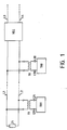
- the transmission system shown in Fig. 1 includes a plurality of transmitter circuits TR1/8 which are coupled in parallel to a transmission line L1, L2. More particularly, each of these transmitter circuits TR1 to TR8 has an output, with terminals L11, L21 to L18, L28, which is coupled to the line L1, L2 through a respective transformer T1/8. At its one end the transmission line L1, L2 is connected to a receiver circuit REC which is coupled to a digital exchange (not shown) through a subscriber line L3, L4, whilst at its other end it is terminated by an impedance Z1.
- Each of the transmitter circuits TR1/8 as well as the receiver circuit REC forms part of an S-interface circuit (not shown) which is able to perform the functions described above, e.g. to generate a current I, or -I, or no current between its output terminals L11 and L21/L18 and L28.
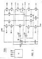
- the transmitter circuits TR1 to TR8 are indentical and therefore only one of them, i.e. TR1, and an associated control circuit CC which together with TR1 forms part of an S-interface is represented in detail in Fig. 2.
- the control circuit CC provides control signals X, XB, Y and YB which directly control the gates of the transistors P3 to P8 and N3 to N6.
- XB and YB are the inverse of X and Y respectively.
- the current source CS2 is in fact derived by current mirroring (not shown) from the accurate current source CS1. In this way a DC resistance which is not very accurate but sufficiently accurate is realised in a simple way.
- Their junction point A is connected to the non-inverting input of operational amplifier OA1 whose inverting input is connected to the junction point B of two parallel circuits which are both connected in series with resistor R2 between VDD and VSS.
- the first of these parallel circuits comprises the series connection of the source-to-drain paths of transistors P1 and P9 and the drain-to-source path of transistor N2.
- the second of these parallel circuits comprises the series connection of the source-to-drain paths of transistors P2 and P9 and the drain-to-source path of transistor N1.
- the gate of transistor P8 is controlled by the output signal of the operational amplifier OA2 whose inverting input is connected to the reference voltage VR and the non-inverting input C of which is connected to the like named junction point C of transistors P7 and P8 which together with the transistor P1/6 and N1/N6 constitute a switching circuit.
- the drain-to-source paths of the transistors P7 and P8 are connected between terminal L11 and C and between terminal L21 and C respectively and their gates are controlled by the control signals X and Y respectively.
- the gates of transistors P1, P2, N1, N2 are controlled by the transistors P3 to P6 and N3 to N6 and permit the flow of current from the end L11 to the end L21 of P9 or vice-versa. More particularly, the source-to-drain paths of transistors P3 and P4 as well as the source-to-drain paths of transistors P5 and P6 are connected in series with the constant current source CS2 between VDD and VSS, and the junction points of P3 and P4 and of P5 and P6 are connected to the gates of P1 and P2 respectively.
- the gates of P3, P4, P5 and P6 are controlled by the respective control signals YB, XB, XB and YB provided by the control circuit CC.
- the gates of transistors N1 and N2 are controlled by the transistors N3, N4 and N5, N6 respectively.
- the drain-to-source paths of transistors N3 and N4 as well as the drain-to-source paths of transistors N5 and N6 are connected in series between the output of operational amplifier OA1 and VSS, and the junction points of N3 and N4 and of N5 and N6 are connected to the gates of N1 and N2 respectively.
- the gates of N3, N4, N5 and N6 are controlled by the respective control signals Y, X, X and Y provided by the control circuit CC.
- the operational amplifier OA2 together with the transistors P7, P8 and P9 constitutes a servo control circuit of which the forward path includes transistor P9 and the feedback path includes transistor P7.
- the operational amplifier OA1 has an input A to which the fixed voltage VA is applied and a feedback path which is closed via N3, N1 or via N5, N2.
- This operational amplifier OA1 together with R2 constitutes a constant current source by which the constant current I1 provided by CS1 is converted to a constant current I in R2.
- This current I flows from VDD to VSS via transistor P1, terminal L11, primary winding of transformer T1, terminal L21, transistor N2 and resistance R2.
- the constant current I1 is converted in the current I by multiplication with the ratio R1/R2. Because the current I1 may thus be chosen relatively small, the power consumption of the whole transmitter circuit is limited. On the other hand it is easier to realise an accurate ratio of resistances than to make accurate resistances.
- n 2.
- the output of the amplifier OA2 is therefore positive due to which transistor P9 is blocked.
- the voltage V across the terminals L11, L21 is limited to a constant value as soon as the current supplied to the receiver circuit REC is at least equal to 2I′.
- the above described switching circuit P1/6, N1/6 in fact consists of four similar electronic contact devices P1/3/4, P2/5/6, N1/4/3 and N2/6/5.
- Each of these devices, for instance P1/3/4 includes : - a main transistor switch P1 which is connected with its source and drain elctrodes between first and second terminals and which has a control third terminal constituted by its gate; - first and second auxiliary transistor switches P3 and P4 which are connected with their source and drain electrodes between said third terminal and a fourth terminal and between said third terminal and a fifth terminal respectively; - control means (CC) to bring said first and second auxiliary transistor switches P3 and P4 in opposite conditions, wherein the one is blocked and the other is conductive.
- CC control means
Priority Applications (1)
| Application Number | Priority Date | Filing Date | Title |
|---|---|---|---|
| AT88202851T ATE103747T1 (de) | 1987-12-23 | 1988-12-13 | Sendeschaltung. |
Applications Claiming Priority (2)
| Application Number | Priority Date | Filing Date | Title |
|---|---|---|---|
| BE8701480A BE1001413A6 (nl) | 1987-12-23 | 1987-12-23 | Zendketen en daarin gebruikt electronisch contactsysteem. |
| BE8701480 | 1987-12-23 |
Publications (3)
| Publication Number | Publication Date |
|---|---|
| EP0322025A2 true EP0322025A2 (de) | 1989-06-28 |
| EP0322025A3 EP0322025A3 (en) | 1990-04-25 |
| EP0322025B1 EP0322025B1 (de) | 1994-03-30 |
Family
ID=3883027
Family Applications (1)
| Application Number | Title | Priority Date | Filing Date |
|---|---|---|---|
| EP88202851A Expired - Lifetime EP0322025B1 (de) | 1987-12-23 | 1988-12-13 | Sendeschaltung |
Country Status (6)
| Country | Link |
|---|---|
| EP (1) | EP0322025B1 (de) |
| AT (1) | ATE103747T1 (de) |
| AU (1) | AU613434B2 (de) |
| BE (1) | BE1001413A6 (de) |
| DE (1) | DE3888810T2 (de) |
| ES (1) | ES2053716T3 (de) |
Cited By (2)
| Publication number | Priority date | Publication date | Assignee | Title |
|---|---|---|---|---|
| EP0325391A2 (de) * | 1988-01-22 | 1989-07-26 | Advanced Micro Devices, Inc. | Pseudoternärkode-Sender |
| US20130287085A1 (en) * | 2011-09-23 | 2013-10-31 | Intel Corporation | Push-pull source-series terminated transmitter apparatus and method |
Citations (3)
| Publication number | Priority date | Publication date | Assignee | Title |
|---|---|---|---|---|
| US3541239A (en) * | 1967-04-18 | 1970-11-17 | English Electric Computers Ltd | Data transmitter utilizing a parallel pair of intermittently energized transformers without saturation |
| US3757168A (en) * | 1970-05-08 | 1973-09-04 | F Kreuzer | Rom disturbances apparatus for protecting data processing installations and the like f |
| US4620310A (en) * | 1985-03-11 | 1986-10-28 | Metapath Inc. | Method and apparatus for generating bipolar pulses in a local area network |
-
1987
- 1987-12-23 BE BE8701480A patent/BE1001413A6/nl not_active IP Right Cessation
-
1988
- 1988-12-05 AU AU26527/88A patent/AU613434B2/en not_active Ceased
- 1988-12-13 DE DE3888810T patent/DE3888810T2/de not_active Expired - Fee Related
- 1988-12-13 EP EP88202851A patent/EP0322025B1/de not_active Expired - Lifetime
- 1988-12-13 AT AT88202851T patent/ATE103747T1/de not_active IP Right Cessation
- 1988-12-13 ES ES88202851T patent/ES2053716T3/es not_active Expired - Lifetime
Patent Citations (3)
| Publication number | Priority date | Publication date | Assignee | Title |
|---|---|---|---|---|
| US3541239A (en) * | 1967-04-18 | 1970-11-17 | English Electric Computers Ltd | Data transmitter utilizing a parallel pair of intermittently energized transformers without saturation |
| US3757168A (en) * | 1970-05-08 | 1973-09-04 | F Kreuzer | Rom disturbances apparatus for protecting data processing installations and the like f |
| US4620310A (en) * | 1985-03-11 | 1986-10-28 | Metapath Inc. | Method and apparatus for generating bipolar pulses in a local area network |
Non-Patent Citations (1)
| Title |
|---|
| IEEE INTERNATIONAL CONFERENCE ON COMMUNICATIONS 1986, Toronto, CA, 22nd-25th June 1986, vol. 1 of 3, pages 336-340, IEEE, New York, US; L.M. SMITH: "ISDN user-network interfaces (layer 1)" * |
Cited By (5)
| Publication number | Priority date | Publication date | Assignee | Title |
|---|---|---|---|---|
| EP0325391A2 (de) * | 1988-01-22 | 1989-07-26 | Advanced Micro Devices, Inc. | Pseudoternärkode-Sender |
| EP0325391A3 (en) * | 1988-01-22 | 1990-05-02 | Advanced Micro Devices, Inc. | Pseudo-ternary code transmitter |
| US20130287085A1 (en) * | 2011-09-23 | 2013-10-31 | Intel Corporation | Push-pull source-series terminated transmitter apparatus and method |
| US9210011B2 (en) * | 2011-09-23 | 2015-12-08 | Intel Corporation | Push-pull source-series terminated transmitter apparatus and method |
| TWI549438B (zh) * | 2011-09-23 | 2016-09-11 | 英特爾公司 | 推挽式源極串聯終端的發射器設備及方法 |
Also Published As
| Publication number | Publication date |
|---|---|
| EP0322025A3 (en) | 1990-04-25 |
| ATE103747T1 (de) | 1994-04-15 |
| EP0322025B1 (de) | 1994-03-30 |
| DE3888810D1 (de) | 1994-05-05 |
| ES2053716T3 (es) | 1994-08-01 |
| AU2652788A (en) | 1989-06-29 |
| DE3888810T2 (de) | 1994-08-18 |
| BE1001413A6 (nl) | 1989-10-24 |
| AU613434B2 (en) | 1991-08-01 |
Similar Documents
| Publication | Publication Date | Title |
|---|---|---|
| US4173714A (en) | Communication circuit with combined power feed and data transmission over a phantom channel | |
| EP0247675B1 (de) | Sender für S-Bus-Schnittstelle in einem dienstintegrierenden Digitalnetz (ISDN) | |
| WO1980001008A1 (en) | Coupling circuit for transferring data signals at a high rate | |
| US2662122A (en) | Two-way transistor electrical transmission system | |
| EP0721254A2 (de) | CMOS-PECL-Pegelumsetzungsschaltung | |
| US2829203A (en) | Electronic telephone subscriber's line circuit for neutralizing the effects of longitudinal induction and longitudinal unbalance | |
| EP0322025B1 (de) | Sendeschaltung | |
| JPS63155931A (ja) | デジタル信号伝送回路 | |
| GB1134371A (en) | Circuit arrangement for simultaneous signalling in both transmission directions between two terminal stations in telecommunication systems | |
| US3476879A (en) | Line relay for d.c. telegraph systems | |
| US4361732A (en) | Trunk interface circuit with current compensation | |
| KR100408746B1 (ko) | 직류전압및교류전압디커플링용회로장치 | |
| US4012590A (en) | Circuit arrangement for two-wire full duplex data transmission | |
| US3849607A (en) | Polarity reversal switching circuit | |
| US3363191A (en) | Data transmission amplifier | |
| US3689710A (en) | Two-wire to four-wire conversion circuit for a data switching center | |
| US4899114A (en) | Voltage source amplifier for use in a pseudoternary code transmitter | |
| US6181167B1 (en) | Full duplex CMOS communication | |
| IE811646L (en) | Circuit arrangement | |
| US4110565A (en) | Duplex telephone signalling system | |
| JPH04213261A (ja) | 電話線の線路終端形成方法および装置 | |
| US2473346A (en) | Teletypewriter exchange system | |
| US2829205A (en) | Duplex signaling circuit | |
| US3823271A (en) | Polarity reversal circuit | |
| EP0271947B1 (de) | Verstärkungsregelschaltung |
Legal Events
| Date | Code | Title | Description |
|---|---|---|---|
| PUAI | Public reference made under article 153(3) epc to a published international application that has entered the european phase |
Free format text: ORIGINAL CODE: 0009012 |
|
| AK | Designated contracting states |
Kind code of ref document: A2 Designated state(s): AT BE CH DE ES FR GB IT LI NL SE |
|
| PUAL | Search report despatched |
Free format text: ORIGINAL CODE: 0009013 |
|
| AK | Designated contracting states |
Kind code of ref document: A3 Designated state(s): AT BE CH DE ES FR GB IT LI NL SE |
|
| RHK1 | Main classification (correction) |
Ipc: H04L 25/08 |
|
| 17P | Request for examination filed |
Effective date: 19901019 |
|
| 17Q | First examination report despatched |
Effective date: 19920907 |
|
| GRAA | (expected) grant |
Free format text: ORIGINAL CODE: 0009210 |
|
| AK | Designated contracting states |
Kind code of ref document: B1 Designated state(s): AT BE CH DE ES FR GB IT LI NL SE |
|
| REF | Corresponds to: |
Ref document number: 103747 Country of ref document: AT Date of ref document: 19940415 Kind code of ref document: T |
|
| REF | Corresponds to: |
Ref document number: 3888810 Country of ref document: DE Date of ref document: 19940505 |
|
| ITF | It: translation for a ep patent filed |
Owner name: DOTT. ANTONIO SERGI |
|
| ET | Fr: translation filed | ||
| REG | Reference to a national code |
Ref country code: ES Ref legal event code: FG2A Ref document number: 2053716 Country of ref document: ES Kind code of ref document: T3 |
|
| EAL | Se: european patent in force in sweden |
Ref document number: 88202851.7 |
|
| PLBE | No opposition filed within time limit |
Free format text: ORIGINAL CODE: 0009261 |
|
| STAA | Information on the status of an ep patent application or granted ep patent |
Free format text: STATUS: NO OPPOSITION FILED WITHIN TIME LIMIT |
|
| 26N | No opposition filed | ||
| PGFP | Annual fee paid to national office [announced via postgrant information from national office to epo] |
Ref country code: GB Payment date: 19981112 Year of fee payment: 11 |
|
| PGFP | Annual fee paid to national office [announced via postgrant information from national office to epo] |
Ref country code: FR Payment date: 19981113 Year of fee payment: 11 |
|
| PGFP | Annual fee paid to national office [announced via postgrant information from national office to epo] |
Ref country code: SE Payment date: 19981118 Year of fee payment: 11 Ref country code: DE Payment date: 19981118 Year of fee payment: 11 |
|
| PGFP | Annual fee paid to national office [announced via postgrant information from national office to epo] |
Ref country code: NL Payment date: 19981123 Year of fee payment: 11 Ref country code: AT Payment date: 19981123 Year of fee payment: 11 |
|
| PGFP | Annual fee paid to national office [announced via postgrant information from national office to epo] |
Ref country code: CH Payment date: 19981124 Year of fee payment: 11 |
|
| PGFP | Annual fee paid to national office [announced via postgrant information from national office to epo] |
Ref country code: BE Payment date: 19981209 Year of fee payment: 11 |
|
| PGFP | Annual fee paid to national office [announced via postgrant information from national office to epo] |
Ref country code: ES Payment date: 19981216 Year of fee payment: 11 |
|
| PG25 | Lapsed in a contracting state [announced via postgrant information from national office to epo] |
Ref country code: GB Free format text: LAPSE BECAUSE OF NON-PAYMENT OF DUE FEES Effective date: 19991213 Ref country code: AT Free format text: LAPSE BECAUSE OF NON-PAYMENT OF DUE FEES Effective date: 19991213 |
|
| PG25 | Lapsed in a contracting state [announced via postgrant information from national office to epo] |
Ref country code: SE Free format text: LAPSE BECAUSE OF NON-PAYMENT OF DUE FEES Effective date: 19991214 |
|
| PG25 | Lapsed in a contracting state [announced via postgrant information from national office to epo] |
Ref country code: LI Free format text: LAPSE BECAUSE OF NON-PAYMENT OF DUE FEES Effective date: 19991231 Ref country code: CH Free format text: LAPSE BECAUSE OF NON-PAYMENT OF DUE FEES Effective date: 19991231 Ref country code: BE Free format text: LAPSE BECAUSE OF NON-PAYMENT OF DUE FEES Effective date: 19991231 |
|
| BERE | Be: lapsed |
Owner name: ALCATEL BELL Effective date: 19991231 |
|
| PG25 | Lapsed in a contracting state [announced via postgrant information from national office to epo] |
Ref country code: NL Free format text: LAPSE BECAUSE OF NON-PAYMENT OF DUE FEES Effective date: 20000701 |
|
| GBPC | Gb: european patent ceased through non-payment of renewal fee |
Effective date: 19991213 |
|
| EUG | Se: european patent has lapsed |
Ref document number: 88202851.7 |
|
| PG25 | Lapsed in a contracting state [announced via postgrant information from national office to epo] |
Ref country code: FR Free format text: LAPSE BECAUSE OF NON-PAYMENT OF DUE FEES Effective date: 20000831 |
|
| NLV4 | Nl: lapsed or anulled due to non-payment of the annual fee |
Effective date: 20000701 |
|
| PG25 | Lapsed in a contracting state [announced via postgrant information from national office to epo] |
Ref country code: DE Free format text: LAPSE BECAUSE OF NON-PAYMENT OF DUE FEES Effective date: 20001003 |
|
| REG | Reference to a national code |
Ref country code: FR Ref legal event code: ST |
|
| PG25 | Lapsed in a contracting state [announced via postgrant information from national office to epo] |
Ref country code: ES Free format text: LAPSE BECAUSE OF NON-PAYMENT OF DUE FEES Effective date: 20001214 |
|
| REG | Reference to a national code |
Ref country code: ES Ref legal event code: FD2A Effective date: 20010113 |
|
| PG25 | Lapsed in a contracting state [announced via postgrant information from national office to epo] |
Ref country code: IT Free format text: LAPSE BECAUSE OF NON-PAYMENT OF DUE FEES;WARNING: LAPSES OF ITALIAN PATENTS WITH EFFECTIVE DATE BEFORE 2007 MAY HAVE OCCURRED AT ANY TIME BEFORE 2007. THE CORRECT EFFECTIVE DATE MAY BE DIFFERENT FROM THE ONE RECORDED. Effective date: 20051213 |