EP0318259B1 - Software-konfigurierbarer Speicher für ein Datenverarbeitungssystem mit graphischer Tätigkeit - Google Patents
Software-konfigurierbarer Speicher für ein Datenverarbeitungssystem mit graphischer Tätigkeit Download PDFInfo
- Publication number
- EP0318259B1 EP0318259B1 EP88311067A EP88311067A EP0318259B1 EP 0318259 B1 EP0318259 B1 EP 0318259B1 EP 88311067 A EP88311067 A EP 88311067A EP 88311067 A EP88311067 A EP 88311067A EP 0318259 B1 EP0318259 B1 EP 0318259B1
- Authority
- EP
- European Patent Office
- Prior art keywords
- graphics
- memory
- address space
- data processing
- framebuffer
- Prior art date
- Legal status (The legal status is an assumption and is not a legal conclusion. Google has not performed a legal analysis and makes no representation as to the accuracy of the status listed.)
- Expired - Lifetime
Links
- 238000012545 processing Methods 0.000 title claims description 33
- 238000003491 array Methods 0.000 claims description 23
- 238000005192 partition Methods 0.000 claims description 13
- 238000000034 method Methods 0.000 claims description 5
- 238000000638 solvent extraction Methods 0.000 claims description 2
- 239000000872 buffer Substances 0.000 description 19
- 238000013461 design Methods 0.000 description 10
- 238000009877 rendering Methods 0.000 description 8
- 230000006870 function Effects 0.000 description 6
- 238000013507 mapping Methods 0.000 description 4
- 238000012546 transfer Methods 0.000 description 4
- 238000010586 diagram Methods 0.000 description 3
- 230000005540 biological transmission Effects 0.000 description 2
- 230000008859 change Effects 0.000 description 2
- 238000006243 chemical reaction Methods 0.000 description 1
- 239000003086 colorant Substances 0.000 description 1
- 230000003247 decreasing effect Effects 0.000 description 1
- 230000001419 dependent effect Effects 0.000 description 1
- 238000001514 detection method Methods 0.000 description 1
- 238000011161 development Methods 0.000 description 1
- 230000018109 developmental process Effects 0.000 description 1
- 230000000694 effects Effects 0.000 description 1
- 238000012544 monitoring process Methods 0.000 description 1
- 230000004044 response Effects 0.000 description 1
- 230000009466 transformation Effects 0.000 description 1
Images


Classifications
-
- G—PHYSICS
- G09—EDUCATION; CRYPTOGRAPHY; DISPLAY; ADVERTISING; SEALS
- G09G—ARRANGEMENTS OR CIRCUITS FOR CONTROL OF INDICATING DEVICES USING STATIC MEANS TO PRESENT VARIABLE INFORMATION
- G09G5/00—Control arrangements or circuits for visual indicators common to cathode-ray tube indicators and other visual indicators
- G09G5/36—Control arrangements or circuits for visual indicators common to cathode-ray tube indicators and other visual indicators characterised by the display of a graphic pattern, e.g. using an all-points-addressable [APA] memory
- G09G5/39—Control of the bit-mapped memory
-
- G—PHYSICS
- G09—EDUCATION; CRYPTOGRAPHY; DISPLAY; ADVERTISING; SEALS
- G09G—ARRANGEMENTS OR CIRCUITS FOR CONTROL OF INDICATING DEVICES USING STATIC MEANS TO PRESENT VARIABLE INFORMATION
- G09G2360/00—Aspects of the architecture of display systems
- G09G2360/12—Frame memory handling
- G09G2360/123—Frame memory handling using interleaving
-
- G—PHYSICS
- G09—EDUCATION; CRYPTOGRAPHY; DISPLAY; ADVERTISING; SEALS
- G09G—ARRANGEMENTS OR CIRCUITS FOR CONTROL OF INDICATING DEVICES USING STATIC MEANS TO PRESENT VARIABLE INFORMATION
- G09G5/00—Control arrangements or circuits for visual indicators common to cathode-ray tube indicators and other visual indicators
- G09G5/36—Control arrangements or circuits for visual indicators common to cathode-ray tube indicators and other visual indicators characterised by the display of a graphic pattern, e.g. using an all-points-addressable [APA] memory
- G09G5/363—Graphics controllers
Definitions
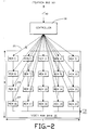
- the processor can directly address a pixel in the framebuffer with an i/o space address; the module addressing means responds by providing location address signals specifying array origin, and mask information signals specifying offset within the specified array.
- the controller is responsive to the mask information signals to select from the transferred update array signals, pixel signals specified by the processor address signal, or to write processor data signals to the location specified by the processor address signal.
- the interface arbitrates among processor system memory operation requests and controller atomic graphics operations.
- each controller is initialized with initializing signals specifying the size of the update array (values of W and H) and the position in the update array of the pixels stored in the chip bank managed by the controller.
- initializing signals are stored at 107 (Fig. 9).
- all data signals for atomic graphics operations are provided in common to all controllers; each controller interprets the data uniquely with respect to its stored initializing signals.
- a controller select signal 95 is output to state machines 100 from module addressing means 17.
Landscapes
- Engineering & Computer Science (AREA)
- Physics & Mathematics (AREA)
- Computer Hardware Design (AREA)
- General Physics & Mathematics (AREA)
- Theoretical Computer Science (AREA)
- Controls And Circuits For Display Device (AREA)
- Image Input (AREA)
- Image Processing (AREA)
- Memory System (AREA)
- Digital Computer Display Output (AREA)
- Image Generation (AREA)
Claims (7)
- Datenverarbeitungssystem, das folgendes aufweist:
eine Datenverarbeitungseinheit (50);
ein Speichermodul (20);
eine Aufteilungseinrichtung (56), die mit der Datenverarbeitungseinheit gekoppelt ist, zum Speichern eines Grenzadressenwerts; und
ein Graphik-Untersystem (10), das mit der Datenverarbeitungseinheit gekoppelt ist;
dadurch gekennzeichnet, daß
das Speichermodul (20) eine Matrix von K Speicherelementen (24) enthält, auf die gleichzeitig zugreifbar ist, wobei jedes Speicherelement eine Vielzahl von Datenwerten an bestimmten Adreßstellen in einem vorbestimmten Adreßraum speichert, wobei der vorbestimmte Adreßraum in zwei Teile einschließlich eines Graphik-Adreßraums und eines Systemspeicher-Adreßraums aufgeteilt ist, wobei K eine ganze Zahl mit einem Wert von wenigstens vier ist;
der Grenzadressenwert, der in der Aufteilungseinrichtung gespeichert ist, eine Grenze zwischen dem Graphik-Adreßraum und dem Systemspeicher-Adreßraum bezeichnet; und
das Graphik-Untersystem (10) folgendes enthält:
einen Satz von K parallelen Graphik-Prozessoren (104), die mit der Datenverarbeitungseinheit und dem Speichermodul gekoppelt sind, zum Speichern und Erneuern von Pixelwerten, die Pixel (x, y) eines X x Y - Raster-Rahmenpuffers (26) in dem Graphik-Adreßraum des Speichermoduls bestimmen, wobei der Satz von K parallelen Graphik-Prozessoren (104), der mit den K Speicherelementen (24) zum gleichzeitigen Zugreifen auf eine und zum Erneuern einer Erneuerungsmatrix von K Pixelwerten gekoppelt ist, wobei der Rahmenpuffer als eine Vielzahl von Erneuerungsmatrizen sequentiell adressierbar ist, die den Rahmenpuffer abdecken, einschließlich einer Vielzahl von horizontalen Reihen der Erneuerungsmatrizen, die eine Matrix der Erneuerungsmatrizen bilden; und
eine Systemspeicher-Zugriffseinrichtung (12, 17, 18) zum Lesen und Speichern von Daten in bestimmten Adreßstellen in dem Systemspeicher-Adreßraum des Speichermoduls und zum Übertragen der gelesenen und gespeicherten Daten zu und von der Datenverarbeitungseinheit;
wobei jedes der K Speicherelemente eine Vielzahl von Datenwerten an Stellen in dem Graphik-Adreßraum und eine Vielzahl von Datenwerten in Stellen in dem Systemspeicher-Adreßraum speichert. - Datenverarbeitungssystem nach Anspruch 1, weiterhin dadurch gekennzeichnet, daß
die Datenverarbeitungseinheit (50) eine Einrichtung zum Senden von Befehlen zu dem Graphik-Untersystem (10) enthält, wobei die Befehle Systemspeicher-Zugriffsbefehle und Graphikbefehle enthalten;
das Graphik-Untersystem (10) eine Schnittstelleneinrichtung (12) enthält, die mit der Datenverarbeitungseinheit (50), den Graphik-Prozessoren und der Systemspeicher-Zugriffseinrichtung gekoppelt ist, zum Empfangen von Befehlen von der Datenverarbeitungseinheit, zum Übertragen von Graphik-Befehlen zu dem Graphik-Untersystem und zum Übertragen von SystemspeicherZugriffsbefehlen zu der Systemspeicher-Zugriffseinrichtung. - Datenverarbeitungssystem nach Anspruch 1 oder 2, weiterhin dadurch gekennzeichnet, daß
der Graphik-Adreßraum und der Systemspeicher-Adreßraum Größen haben, die durch den Grenzadressenwert definiert sind, der in der Aufteilungseinrichtung (56) gespeichert ist; und die Datenverarbeitungseinheit (50) eine Einrichtung enthält zum Ändern des Grenzadressenwerts, der in der Aufteilungseinrichtung gespeichert ist, und dadurch die Adreßraumgrößen des Graphik-Adreßraums und des Systemspeicher-Adreßraums ändert. - Datenverarbeitungssystem nach Anspruch 1, weiterhin dadurch gekennzeichnet, daß
das Graphik-Untersystem (10) eine Ausgangsschaltung (22) enthält zum Zugreifen auf den X x Y - Raster-Rahmenpuffer (26) in dem Graphik-Adreßraum des Speichermoduls und zum Ausgeben entsprechenden Anzeige-Steuersignale zu einer Anzeigevorrichtung. - Verfahren zum Betreiben eines Datenverarbeitungssystems mit einer Datenverarbeitungseinheit (50), einem Speichermodul (20), einer Aufteilungseinrichtung (56), die mit der Datenverarbeitungseinheit gekoppelt ist, zum Speichern eines Grenzadressenwerts, und einem Graphik-Untersystem (10), das mit der Datenverarbeitungseinheit gekoppelt ist, wobei das Verfahren folgendes aufweist:
Speichern von Graphikdaten in dem Speichermodul; und
Zugreifen auf die Graphikdaten in dem Speichermodul und Ausgeben entsprechender Anzeige-Steuersignale zu einer Anzeigevorrichtung;
gekennzeichnet durch
Bereitstellen des Speichermoduls (20) als eine Matrix von K Speicherelementen (24), auf die gleichzeitig zugreifbar ist, wobei jedes Speicherelement eine Vielzahl von Datenwerten an bestimmten Adreßstellen in einem vorbestimmten Adreßraum speichert, wobei K eine ganze Zahl mit einem Wert von wenigstens vier ist;
Aufteilen des vorbestimmten Adreßraums in zwei Teile einschließlich eines Graphik-Adreßraums und eines Systemspeicher-Adreßraums durch Speichern des Grenzadressenwerts in der Aufteilungseinrichtung, der eine Grenze zwischen dem Graphik-Adreßraum und dem Systemspeicher-Adreßraum bezeichnet;
Bereitstellen eines Satzes von K parallelen Graphik-Prozessoren (104) in dem Graphik-Untersystem (10), die mit der Datenverabeitungseinheit und K Speicherlementen (24) gekoppelt sind, zum Speichern und Erneuern von Pixelwerten, die Pixel (x, y) eines X x Y - Raster-Rahmenpuffers (26) in dem Graphik-Adreßraum des Speichermoduls bestimmen; wobei der Rahmenpuffer als eine Vielzahl von Erneuerungsmatrizen sequentiell adressierbar ist, die den Rahmenpuffer abdecken, einschließlich einer Vielzahl von horizontalen Reihen von Erneuerungsmatrizen, die eine Matrix der Erneuerungsmatrizen bilden;
wobei der Satz von K parallelen Graphik-Prozessoren (104), die mit den K Speicherelementen (24) gekoppelt sind, gleichzeitig auf eine Erneuerungsmatrix von K Pixelwerten zugreifen und sie erneuern; und
Lesen und Speichern von Daten in bestimmten Aureßstellen in dem Systemspeicher-Adreßraum des Speichermoduls und Übertragen der gelesenen und gespeicherten Daten zu und von der Datenverarbeitungseinheit;
wobei jedes der K Speicherelemente eine Vielzahl von Datenwerten an Stellen in dem Graphik-Adreßraum und eine Vielzahl von Datenwerten in Stellen in dem Systemspeicher-Adreßraum speichert. - Verfahren nach Anspruch 5, weiterhin dadurch gekennzeichnet, daß die Datenverarbeitungseinheit (50) Befehle zu dem Graphik-Untersystem (10) sendet, wobei die Befehle SystemspeicherZugriffsbefehle und Graphikbefehle enthalten;
das Graphik-Untersystem (10) die Befehle von der Datenverarbeitungseinheit empfängt, die Graphikbefehle zu dem Graphik-Untersystem überträgt und auf Systemspeicher-Zugriffsbefehle durch Lesen und Speichern von Daten in bestimmten Adreßstellen in dem Systemspeicher-Adreßraum des Speichermoduls antwortet und die gelesenen und gespeicherten Daten zu und von der Datenverarbeitungseinheit überträgt. - Verfahren nach Anspruch 5 oder 6, weiterhin dadurch gekennzeichnet, daß
der Graphik-Adreßraum und der Systemspeicher-Adreßraum Größen haben, die durch den in der Aufteilungseinrichtung (56) gespeicherten Grenzadressenwert definiert sind;
die Grenzadressenwerte, die in der Aufteilungseinrichtung gespeichert sind, geändert werden und dadurch die Adreßraumgrößen des Graphik-Adreßraums und des Systemspeicher-Adreßraums geändert werden.
Applications Claiming Priority (2)
| Application Number | Priority Date | Filing Date | Title |
|---|---|---|---|
| US124897 | 1987-11-24 | ||
| US07/124,897 US4953101A (en) | 1987-11-24 | 1987-11-24 | Software configurable memory architecture for data processing system having graphics capability |
Publications (3)
| Publication Number | Publication Date |
|---|---|
| EP0318259A2 EP0318259A2 (de) | 1989-05-31 |
| EP0318259A3 EP0318259A3 (de) | 1991-07-24 |
| EP0318259B1 true EP0318259B1 (de) | 1995-02-08 |
Family
ID=22417328
Family Applications (1)
| Application Number | Title | Priority Date | Filing Date |
|---|---|---|---|
| EP88311067A Expired - Lifetime EP0318259B1 (de) | 1987-11-24 | 1988-11-23 | Software-konfigurierbarer Speicher für ein Datenverarbeitungssystem mit graphischer Tätigkeit |
Country Status (5)
| Country | Link |
|---|---|
| US (1) | US4953101A (de) |
| EP (1) | EP0318259B1 (de) |
| JP (1) | JP2683564B2 (de) |
| CA (1) | CA1312963C (de) |
| DE (1) | DE3852989T2 (de) |
Families Citing this family (40)
| Publication number | Priority date | Publication date | Assignee | Title |
|---|---|---|---|---|
| US5287450A (en) * | 1988-09-29 | 1994-02-15 | Mitsubishi Denki Kabushiki Kaisha | Video signal brancher |
| US5197140A (en) * | 1989-11-17 | 1993-03-23 | Texas Instruments Incorporated | Sliced addressing multi-processor and method of operation |
| US5218678A (en) * | 1989-11-17 | 1993-06-08 | Digital Equipment Corporation | System and method for atomic access to an input/output device with direct memory access |
| US5287452A (en) * | 1990-03-23 | 1994-02-15 | Eastman Kodak Company | Bus caching computer display system |
| JP3350043B2 (ja) * | 1990-07-27 | 2002-11-25 | 株式会社日立製作所 | 図形処理装置及び図形処理方法 |
| ATE208071T1 (de) * | 1990-11-30 | 2001-11-15 | Sun Microsystems Inc | Verfahren und gerät zur darstellung von grafischen bildern |
| CA2070934C (en) * | 1992-06-10 | 1998-05-05 | Benny Chi Wah Lau | Graphics display system |
| US5404448A (en) * | 1992-08-12 | 1995-04-04 | International Business Machines Corporation | Multi-pixel access memory system |
| US5404437A (en) * | 1992-11-10 | 1995-04-04 | Sigma Designs, Inc. | Mixing of computer graphics and animation sequences |
| US6116768A (en) * | 1993-11-30 | 2000-09-12 | Texas Instruments Incorporated | Three input arithmetic logic unit with barrel rotator |
| JPH09507104A (ja) * | 1993-11-30 | 1997-07-15 | ヴィエルエスアイ テクノロジー インコーポレイテッド | 共用メモリシステムの同時動作を可能にし最大にする方法及び装置 |
| WO1995015528A1 (en) * | 1993-11-30 | 1995-06-08 | Vlsi Technology, Inc. | A reallocatable memory subsystem enabling transparent transfer of memory function during upgrade |
| US5515107A (en) * | 1994-03-30 | 1996-05-07 | Sigma Designs, Incorporated | Method of encoding a stream of motion picture data |
| US5598576A (en) * | 1994-03-30 | 1997-01-28 | Sigma Designs, Incorporated | Audio output device having digital signal processor for responding to commands issued by processor by emulating designated functions according to common command interface |
| US5528309A (en) | 1994-06-28 | 1996-06-18 | Sigma Designs, Incorporated | Analog video chromakey mixer |
| TW399189B (en) * | 1994-10-13 | 2000-07-21 | Yamaha Corp | Control device for the image display |
| US5513318A (en) * | 1994-12-28 | 1996-04-30 | At&T Corp. | Method for built-in self-testing of ring-address FIFOs |
| US5790881A (en) * | 1995-02-07 | 1998-08-04 | Sigma Designs, Inc. | Computer system including coprocessor devices simulating memory interfaces |
| TW335466B (en) * | 1995-02-28 | 1998-07-01 | Hitachi Ltd | Data processor and shade processor |
| US6204864B1 (en) | 1995-06-07 | 2001-03-20 | Seiko Epson Corporation | Apparatus and method having improved memory controller request handler |
| US5767866A (en) * | 1995-06-07 | 1998-06-16 | Seiko Epson Corporation | Computer system with efficient DRAM access |
| US5872998A (en) * | 1995-11-21 | 1999-02-16 | Seiko Epson Corporation | System using a primary bridge to recapture shared portion of a peripheral memory of a peripheral device to provide plug and play capability |
| US5719511A (en) * | 1996-01-31 | 1998-02-17 | Sigma Designs, Inc. | Circuit for generating an output signal synchronized to an input signal |
| US5748203A (en) * | 1996-03-04 | 1998-05-05 | United Microelectronics Corporation | Computer system architecture that incorporates display memory into system memory |
| US5818468A (en) * | 1996-06-04 | 1998-10-06 | Sigma Designs, Inc. | Decoding video signals at high speed using a memory buffer |
| US6128726A (en) * | 1996-06-04 | 2000-10-03 | Sigma Designs, Inc. | Accurate high speed digital signal processor |
| US6940496B1 (en) * | 1998-06-04 | 2005-09-06 | Silicon, Image, Inc. | Display module driving system and digital to analog converter for driving display |
| US6145033A (en) * | 1998-07-17 | 2000-11-07 | Seiko Epson Corporation | Management of display FIFO requests for DRAM access wherein low priority requests are initiated when FIFO level is below/equal to high threshold value |
| US6119207A (en) * | 1998-08-20 | 2000-09-12 | Seiko Epson Corporation | Low priority FIFO request assignment for DRAM access |
| US6819321B1 (en) * | 2000-03-31 | 2004-11-16 | Intel Corporation | Method and apparatus for processing 2D operations in a tiled graphics architecture |
| US6611469B2 (en) | 2001-12-11 | 2003-08-26 | Texas Instruments Incorporated | Asynchronous FIFO memory having built-in self test logic |
| US20060177122A1 (en) * | 2005-02-07 | 2006-08-10 | Sony Computer Entertainment Inc. | Method and apparatus for particle manipulation using graphics processing |
| US7627723B1 (en) * | 2006-09-21 | 2009-12-01 | Nvidia Corporation | Atomic memory operators in a parallel processor |
| US9513905B2 (en) | 2008-03-28 | 2016-12-06 | Intel Corporation | Vector instructions to enable efficient synchronization and parallel reduction operations |
| US8688957B2 (en) | 2010-12-21 | 2014-04-01 | Intel Corporation | Mechanism for conflict detection using SIMD |
| US9411592B2 (en) | 2012-12-29 | 2016-08-09 | Intel Corporation | Vector address conflict resolution with vector population count functionality |
| US9411584B2 (en) | 2012-12-29 | 2016-08-09 | Intel Corporation | Methods, apparatus, instructions, and logic to provide vector address conflict detection functionality |
| EP3565259A1 (de) * | 2016-12-28 | 2019-11-06 | Panasonic Intellectual Property Corporation of America | Verteilungsverfahren für dreidimensionales modell, empfangsverfahren für dreidimensionales modell, verteilungsvorrichtung für dreidimensionales modell und empfangsvorrichtung für dreidimensionales modell |
| US20240370361A1 (en) * | 2021-09-07 | 2024-11-07 | Rambus Inc. | Common data strobe among multiple memory devices |
| CN117935707A (zh) * | 2022-10-25 | 2024-04-26 | 华为技术有限公司 | 驱动芯片及电子设备 |
Family Cites Families (8)
| Publication number | Priority date | Publication date | Assignee | Title |
|---|---|---|---|---|
| US3328768A (en) * | 1964-04-06 | 1967-06-27 | Ibm | Storage protection systems |
| US4197590A (en) * | 1976-01-19 | 1980-04-08 | Nugraphics, Inc. | Method for dynamically viewing image elements stored in a random access memory array |
| US4092728A (en) * | 1976-11-29 | 1978-05-30 | Rca Corporation | Parallel access memory system |
| US4432067A (en) * | 1981-05-07 | 1984-02-14 | Atari, Inc. | Memory cartridge for video game system |
| US4608632A (en) * | 1983-08-12 | 1986-08-26 | International Business Machines Corporation | Memory paging system in a microcomputer |
| EP0158209B1 (de) * | 1984-03-28 | 1991-12-18 | Kabushiki Kaisha Toshiba | Speichersteueranordnung für ein Kathodenstrahlanzeigesteuergerät |
| EP0245564B1 (de) * | 1986-05-06 | 1992-03-11 | Digital Equipment Corporation | Multi-Port-Speicher und Quelleneinrichtung für Bildpunktinformation |
| US4773044A (en) * | 1986-11-21 | 1988-09-20 | Advanced Micro Devices, Inc | Array-word-organized display memory and address generator with time-multiplexed address bus |
-
1987
- 1987-11-24 US US07/124,897 patent/US4953101A/en not_active Expired - Lifetime
-
1988
- 1988-11-23 EP EP88311067A patent/EP0318259B1/de not_active Expired - Lifetime
- 1988-11-23 DE DE3852989T patent/DE3852989T2/de not_active Expired - Fee Related
- 1988-11-23 CA CA000583846A patent/CA1312963C/en not_active Expired - Fee Related
- 1988-11-24 JP JP63297175A patent/JP2683564B2/ja not_active Expired - Fee Related
Also Published As
| Publication number | Publication date |
|---|---|
| JPH01302442A (ja) | 1989-12-06 |
| JP2683564B2 (ja) | 1997-12-03 |
| EP0318259A3 (de) | 1991-07-24 |
| DE3852989D1 (de) | 1995-03-23 |
| EP0318259A2 (de) | 1989-05-31 |
| CA1312963C (en) | 1993-01-19 |
| DE3852989T2 (de) | 1995-10-12 |
| US4953101A (en) | 1990-08-28 |
Similar Documents
| Publication | Publication Date | Title |
|---|---|---|
| EP0318259B1 (de) | Software-konfigurierbarer Speicher für ein Datenverarbeitungssystem mit graphischer Tätigkeit | |
| US5488385A (en) | Multiple concurrent display system | |
| US4704697A (en) | Multiple station video memory | |
| US4991110A (en) | Graphics processor with staggered memory timing | |
| US5909225A (en) | Frame buffer cache for graphics applications | |
| EP0447225B1 (de) | Verfahren und Einrichtung zur Maximierung von Spaltenadressenkohärenz für den Zugriff von seriellen und Direktzugriffstoren in einem graphischen System mit einem Rasterpufferspeicher | |
| US5959639A (en) | Computer graphics apparatus utilizing cache memory | |
| US6104418A (en) | Method and system for improved memory interface during image rendering | |
| US5025249A (en) | Pixel lookup in multiple variably-sized hardware virtual colormaps in a computer video graphics system | |
| US4745407A (en) | Memory organization apparatus and method | |
| US5251298A (en) | Method and apparatus for auxiliary pixel color management using monomap addresses which map to color pixel addresses | |
| US5666521A (en) | Method and apparatus for performing bit block transfers in a computer system | |
| US4782462A (en) | Raster scan video controller with programmable prioritized sharing of display memory between update and display processes and programmable memory access termination | |
| JP3639464B2 (ja) | 情報処理システム | |
| JP2001505342A (ja) | 内部メモリ及び外部メモリコントロールを具備したコンピュータシステムコントローラ | |
| KR100227133B1 (ko) | 보존된 어드레싱을 이용하는 메모리 장치 및 이를 이용한 시스템및 방법 | |
| EP0398510B1 (de) | Video-Direktzugriffsspeicher | |
| JPH0690613B2 (ja) | 表示制御装置 | |
| US5216413A (en) | Apparatus and method for specifying windows with priority ordered rectangles in a computer video graphics system | |
| EP0259050A2 (de) | Vielfachkanal-Speicherzugriffsschaltung | |
| US4675842A (en) | Apparatus for the display and storage of television picture information by using a memory accessible from a computer | |
| EP0182454B1 (de) | Steuerlogik für ein Videosystem mit einer Schaltung, welche die Zeilenadresse ausser Kraft setzt | |
| US4912658A (en) | Method and apparatus for addressing video RAMS and refreshing a video monitor with a variable resolution | |
| US4935880A (en) | Method of tiling a figure in graphics rendering system | |
| EP0752694B1 (de) | Verfahren zum schnellen Ausmalen und Kopieren von Bildelementen kurzer Wortlänge in einem breiteren Rasterpufferspeicher |
Legal Events
| Date | Code | Title | Description |
|---|---|---|---|
| PUAI | Public reference made under article 153(3) epc to a published international application that has entered the european phase |
Free format text: ORIGINAL CODE: 0009012 |
|
| AK | Designated contracting states |
Kind code of ref document: A2 Designated state(s): DE FR GB |
|
| PUAL | Search report despatched |
Free format text: ORIGINAL CODE: 0009013 |
|
| AK | Designated contracting states |
Kind code of ref document: A3 Designated state(s): DE FR GB |
|
| 17P | Request for examination filed |
Effective date: 19911018 |
|
| 17Q | First examination report despatched |
Effective date: 19930419 |
|
| GRAA | (expected) grant |
Free format text: ORIGINAL CODE: 0009210 |
|
| AK | Designated contracting states |
Kind code of ref document: B1 Designated state(s): DE FR GB |
|
| REF | Corresponds to: |
Ref document number: 3852989 Country of ref document: DE Date of ref document: 19950323 |
|
| ET | Fr: translation filed | ||
| PLBE | No opposition filed within time limit |
Free format text: ORIGINAL CODE: 0009261 |
|
| STAA | Information on the status of an ep patent application or granted ep patent |
Free format text: STATUS: NO OPPOSITION FILED WITHIN TIME LIMIT |
|
| 26N | No opposition filed | ||
| REG | Reference to a national code |
Ref country code: GB Ref legal event code: 732E |
|
| REG | Reference to a national code |
Ref country code: GB Ref legal event code: IF02 |
|
| REG | Reference to a national code |
Ref country code: GB Ref legal event code: 732E |
|
| PGFP | Annual fee paid to national office [announced via postgrant information from national office to epo] |
Ref country code: GB Payment date: 20070125 Year of fee payment: 19 |
|
| PGFP | Annual fee paid to national office [announced via postgrant information from national office to epo] |
Ref country code: DE Payment date: 20070228 Year of fee payment: 19 |
|
| PGFP | Annual fee paid to national office [announced via postgrant information from national office to epo] |
Ref country code: FR Payment date: 20070207 Year of fee payment: 19 |
|
| GBPC | Gb: european patent ceased through non-payment of renewal fee |
Effective date: 20071123 |
|
| PG25 | Lapsed in a contracting state [announced via postgrant information from national office to epo] |
Ref country code: DE Free format text: LAPSE BECAUSE OF NON-PAYMENT OF DUE FEES Effective date: 20080603 |
|
| REG | Reference to a national code |
Ref country code: FR Ref legal event code: ST Effective date: 20080930 |
|
| PG25 | Lapsed in a contracting state [announced via postgrant information from national office to epo] |
Ref country code: GB Free format text: LAPSE BECAUSE OF NON-PAYMENT OF DUE FEES Effective date: 20071123 |
|
| PG25 | Lapsed in a contracting state [announced via postgrant information from national office to epo] |
Ref country code: FR Free format text: LAPSE BECAUSE OF NON-PAYMENT OF DUE FEES Effective date: 20071130 |